

Page 1
Data Sheet
29317.16E
2557
PROTECTED QUAD LOW-SIDE DRIVER
WITH FAULT DETECTION & SLEEP MODE
The A2557xB, A2557xEB, and A2557xLB have been specifically
designed to provide cost-effective solutions to relay-driving applications with
up to 300 mA drive current per channel. They may also be used for driving
incandescent lamps in applications where turn-on time is not a concern. Each
of the four outputs will sink 300 mA in the on state. The outputs have a
minimum breakdown voltage of 60 V and a sustaining voltage of 40 V. A
low-power Sleep Mode is activated with either ENABLE low or all inputs
low. In this mode, the supply current drops to below 100 µA.
Over-current protection for each channel has been designed into these
devices and is activated at a nominal 500 mA. It protects each output from
short circuits with supply voltages up to 32 V. When an output experiences a
short circuit, the output current is limited at the 500 mA current clamp. In
addition, foldback circuitry decreases the current limit if an excessive voltage
is present across the output and assists in keeping the device within its SOA
(safe operating area). An exclusive-OR circuit compares the input and output
state of each driver. If either a short or open load condition is detected, a
single FAULT output is turned on (active low). Similar devices, for operation
to 1.3 A, are available as the UDx2547B/EB.
Continuous or multiple overload conditions causing the channel temperature to reach approximately 165°C will result in an additional linear decrease
in the output current of the affected driver. If the fault condition is corrected,
the output stage will return to its normal saturated condition.
The first character of the part number suffix determines the device
operating temperature range. Suffix ‘S-’ is the standard -20°C to +85°C;
suffix ‘E-’ is -40°C to +85°C; suffix ‘K-’ is for the industrial temperature
range of -40°C to +125°C. Package suffix ‘-B’ devices are 16-pin power
DIPs; suffix ‘-EB’ devices are 28-lead power PLCCs; and suffix ‘-LB’ are 16lead power wide-body SOICs for surface-mount applications. All packages
are of batwing construction to provide for maximum package power dissipation.
FEATURES
■ 300 mA Output Current per Channel
■ Independent Over-Current Protection &Thermal Limiting for Each Driver
■ Output Voltage to 60 V
■ Output SOA Protection
■ Fault-Detection Circuitry for Open or Shorted Load
■ Low Quiescent Current Sleep Mode
■ Integral Output Flyback/Clamp Diodes
■ TTL- and 5 V CMOS-Compatible Inputs
1
2
3
14
4
5
6
7
8
9
10
11
12
13
15
16
ENABLE
GROUND
GROUND
OUT
3
FAULT
GROUND
GROUND
OUT
2
OUT
1
K
OUT
4
V
CC
IN
4
Dwg. PP-017-4
IN
1
IN
2
IN
3
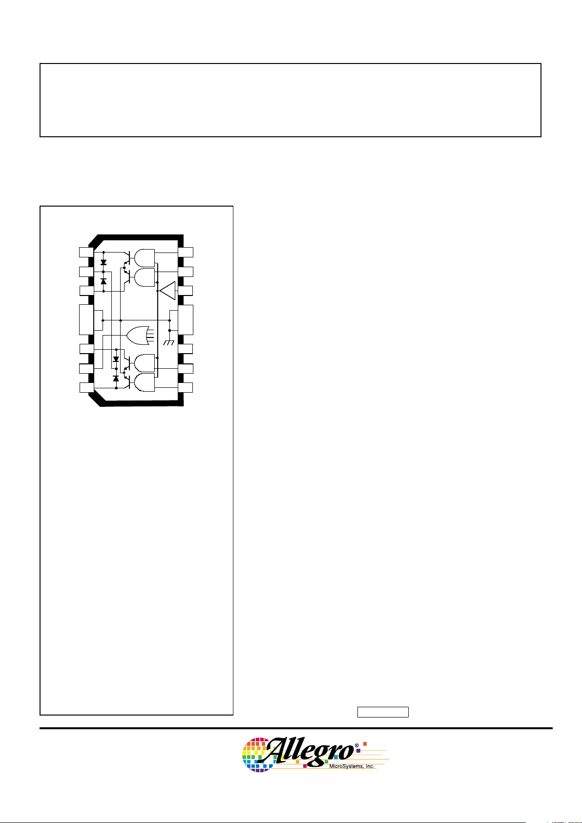
A2557xLB
Note that the A2557xB (DIP) and the A2557xLB
(SOIC) are electrically identical and share a
common terminal number assignment.
ABSOLUTE MAXIMUM RATINGS
Output Voltage, VO.............................. 60 V
Over-Current Protected Output Voltage,
VO..................................................... 32 V
Output Current, IO......................... 500 mA*
FAULT Output Voltage, V
FLT
............. 60 V
Logic Supply Voltage, VCC................. 7.0 V
Input Voltage, VI or VOE..................... 7.0 V
Package Power Dissipation,
PD........................................... See Graph
Operating Temperature Range, T
A
Suffix ‘S-’ ...................... -20°C to +85°C
Suffix ‘E-’ ...................... -40°C to +85°C
Suffix ‘K-’ ................... -40°C to +125°C
Junction Temperature,
TJ............................................... +150°C*
Storage Temperature Range,
TS................................. -55°C to +150°C
*Outputs are current limited at approximately
500 mA per driver and junction temperature
limited if higher current is attempted.
Complete part number includes a suffix to identify operating temperature
range (E-, K-, or S-) and package type (-B, -EB, or -LB). Always order by
complete part number, e.g., A2557KLB .
Page 2
2557
PROTECTED QUAD DRIVER
WITH FAULT DETECTION
& SLEEP MODE
115 Northeast Cutoff, Box 15036
Worcester, Massachusetts 01615-0036 (508) 853-5000
2
Copyright © 1998, 2000, Allegro MicroSystems, Inc.
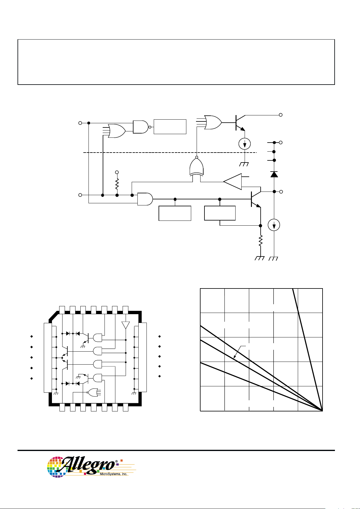
FUNCTIONAL BLOCK DIAGRAM
<<1 Ω
OUT
Dwg. FP-007-2
N
ENABLE
IN
N
FAULT
COMMON CONTROL
ONE OF FOUR DRIVERS
CURRENT
LIMIT
THERMAL
LIMIT
SLEEP
CONTROL
30 µA
60 µA
2.5 V
–
+
K
V
CC
A2557xEB
1
2
3
4
5
6
7
8
9
10
11
12
13
14
15
16
17
18
19
20
21
22
23
24
25
26
27
28
GROUND
GROUND
GROUND
GROUND
Dwg. PP-019-2
NO
CONNECTION
ENABLE
SUPPLY
NC
NC
CC
V
OUT
1
OUT
2
OUT
3
OUT
4
IN
4
IN
3
IN
2
IN
1
NO
CONNECTION
K
FAULT
50 75 100 125 150
5
3
2
1
0
ALLOWABLE PACKAGE POWER DISSIPATION IN WATTS
TEMPERATURE IN °C
4
25
R = 6°C/W
θJT
Dwg. GP-004-2A
SUFFIX 'EB', R = 36°C/W
θJA
SUFFIX 'B', R = 43°C/W
θJA
SUFFIX 'LB', R = 63°C/W
θJA
Page 3

2557
PROTECTED QUAD DRIVER
WITH FAULT DETECTION
& SLEEP MODE
www.allegromicro.com
3
Limits
Characteristic Symbol Test Conditions Min. Typ. Max. Units
Output Leakage Current* I
CEX
VO = 60 V, VI = 0.8 V, VOE = 2.0 V — 30 100 µA
VO = 60 V, VI = 2.0 V, VOE = 0.8 V — <1.0 100 µA
Output Sustaining Voltage V
O(SUS)
IO = 100 mA, VI = VOE = 0.8 V, V
CC
= Open 40 — — V
Output Saturation Voltage V
O(SAT)
IO = 100 mA — 65 200 mV
IO = 300 mA — 180 300 mV
Over-Current Limit I
OM
5 ms PulseTest, VO = 5.0 V — 500 — mA
Input Voltage V
IH
INn or ENABLE 2.0 — — V
V
IL
INn or ENABLE — — 0.8 V
Input Current I
IH
INn or ENABLE, VIH = 2.0 V — — 10 µA
I
IL
INn or ENABLE, VIL = 0.8 V — — -10 µA
Fault Output Leakage Current I
FLT
V
FLT
= 60 V — 4.0 15 µA
V
FLT
= 5 V — <1.0 2.0 µA
Fault Output Current I
FLT
V
FLT =
5 V, Driver Output Open,
VI = 0.8 V, V
OE
= 2.0 V 40 60 80 µ A
Fault Output Saturation Voltage V
FLT(SAT)
I
FLT
= 30 µA — 0.1 0.4 V
Clamp Diode Forward Voltage V
F
IF = 500 mA — 1.2 1.7 V
IF = 750 mA — 1.5 2.1 V
Clamp Diode Leakage Current I
R
VR = 60 V — — 50 µA
Turn-On Delay t
PHL
IO = 300 mA, 50% VI to 50% V
O
— 0.6 10 µs
From Sleep, IO = 300 mA, 50% VI to 50% V
O
— 3.0 — µs
IO = 300 mA, 50% VOE to 50% V
O
— 1.3 10 µs
Turn-Off Delay t
PLH
IO = 300 mA, 50% VI to 50% V
O
— 2.0 10 µs
IO = 300 mA, 50% VOE to 50% V
O
— 1.4 10 µs
Total Supply Current I
CC
All Outputs Off — 0.075 0.1 mA
Any One Output On — 12 20 mA
Two Outputs On — 18 30 mA
Three Outputs On — 24 40 mA
All Outputs On — 30 50 mA
Thermal Limit T
J
— 165 — °C
ELECTRICAL CHARACTERISTICS over operating temperature range, V
CC
= 4.75 V to 5.25 V
Typical Data is at TA = +25°C and VCC = 5 V and is for design information only.
Negative current is defined as coming out of (sourcing) the specified terminal.
As used here, -100 is defined as greater than +10 (absolute magnitude convention) and the minimum is implicitly zero.
* Measurement includes output fault-sensing pull-down current.
Page 4
2557
PROTECTED QUAD DRIVER
WITH FAULT DETECTION
& SLEEP MODE
115 Northeast Cutoff, Box 15036
Worcester, Massachusetts 01615-0036 (508) 853-5000
4
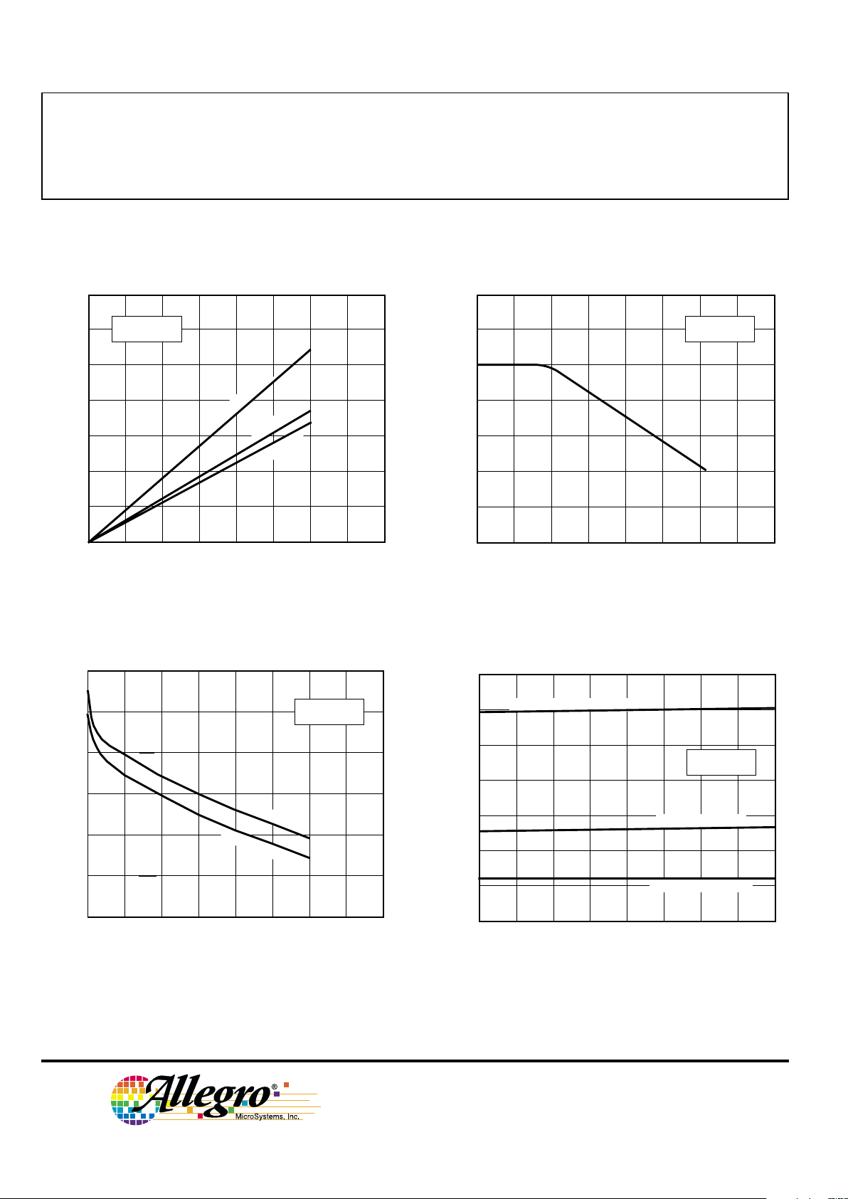
TYPICAL OPERATING CHARACTERISTICS
100
Dwg. GP-064
200
400
300
OUTPUT CURRENT IN MILLIAMPERES
0
0.3
0.2
OUTPUT SATURATION VOLTAGE IN VOLTS
0.1
0
VCC = 5 V
T
A
= 125
°C
T
A
= 25
°C
T
A
=
-4
0
°C
10
Dwg. GP-065
20
40
30
OUTPUT VOLTAGE IN VOLTS
0
600
500
400
300
OUTPUT CURRENT LIMIT IN MILLIAMPERES
TA = +25°C
V
CC
= 5 V
100
Dwg. GP-066-1
200
400
300
OUTPUT CURRENT IN MILLIAMPERES
0
3
2
TURN-ON DELAY IN MICROSECONDS
1
0
TA = +25°C
V
CC
= 5 V
ENABLE SWITCHING
IN SWITCHING (FROM SLEEP)
IN SWITCHING (AWAKE)
100
Dwg. GP-066
200
400
300
OUTPUT CURRENT IN MILLIAMPERES
0
6
4
TURN-OFF DELAY IN MICROSECONDS
2
0
TA = +25°C
V
CC
= 5 V
ENABLE SWITCHING
IN
S
W
IT
C
H
IN
G
Page 5

2557
PROTECTED QUAD DRIVER
WITH FAULT DETECTION
& SLEEP MODE
www.allegromicro.com
5
The A2557 low-current quad power drivers provide the
same protected output driver function as (and are pin compatible with) the UDx2543/49/59 devices, combined with a fault
diagnostic scheme similar to the UDx2547, plus an automatic
low-current Sleep-Mode function. These devices monitor their
outputs for fault (open or shorted) conditions. For each channel
the input and output levels are compared. If these are different
from the expected levels then a fault condition is flagged by
pulling the common FAULT output low.
Status INNENABLE OUT
N
FAULT
Normal Load
HH L H
LH H H
Sleep Mode
XL H H
All L X H H
Over-Current or
Short to Supply
HH R L
Open Load or
Short to Ground
LH L L
Thermal Fault H H H L
R = Linear drive, current limited.
The FAULT output is operational only if ENABLE is high.
The output state is detected by monitoring the OUTn terminal
using a comparator whose threshold is typically 2.5 V. In order
to detect open-circuit outputs, a 30 µA current sink pulls the
output below the comparator threshold. To ensure correct fault
operation, a minimum load of approximately 1 mA is required.
The fault function is disabled when in ‘sleep’ mode, i.e.,
FAULT goes high and the 30 µA output sinks are turned off.
The FAULT output is a switched current sink of typically
60 µA.
Each channel consists of a TTL/CMOS-compatible logic
input gated with a common ENABLE input. A logic high at the
input will provide drive to turn on the output npn switch. Each
output has a current-limit circuit that limits the output current
by detecting the voltage drop across a low-value internal
resistor in the emitter of the output switch. If this drop reaches
a threshold, then the base drive to the output switch is reduced
to maintain constant current in the output.
To keep the device within its safe operating area (SOA) this
output current limit is further reduced
CIRCUIT DESCRIPTION AND APPLICATION
• if the power dissipation in the output device increases the
local junction temperature above 165°C (nominal), so as to limit
the power dissipation (and hence the local junction temperature). As each channel has its own thermal limit circuitry this
provides some independence between the output channels, i.e.,
one channel can be operating in thermally reduced current limit,
while the others can provide full drive capability.
• as a function of the output voltage. Full current limit of
500 mA (nominal) is available up to approximately VO = 8 V;
above this the limit is reduced linearly to about 350 mA at VO =
32 V. This helps to improve SOA by immediately reducing the
peak power pulse into a shorted load at high VO.
A logic low at the ENABLE input causes all outputs to be
switched off regardless of the state of the IN terminals. In
addition, the device is put into a low quiescent current ‘sleep’
mode, reducing ICC below 100 µA. If ENABLE is taken high
and any of the inputs go high, the circuit will ‘auto-wake-up’.
However, if the device is enabled, but all inputs stay low, then
the circuit remains in ‘sleep’ mode.
All outputs have internal flyback diodes, with a commoncathode connection at the K terminal.
Incandescent lamp driver
High incandescent lamp turn-on (in-rush currents) can
contribute to poor lamp reliability and destroy semiconductor
lamp drivers. When an incandescent lamp is initially turned on,
the cold filament is at minimum resistance and would normally
allow a 10x to 12x in-rush current.
Warming (parallel) or current-limiting (series) resistors
protect both driver and lamp but use significant power either
when the lamp is off or when the lamp is on, respectively.
Lamps with steady-state current ratings up to 300 mA can be
driven without the need for warming or current-limiting
resistors, if lamp turn-on time is not a concern (10s of ms).
With these drivers, during turn-on, the high in-rush current
is sensed by the internal sense resistor, drive current to the
output stage is reduced, and the output operates in a linear mode
with the load current limited to approximately 500 mA. During
lamp warmup, the filament resistance increases to its maximum
value, the output driver goes into saturation and applies maximum rated voltage to the lamp.
Page 6

2557
PROTECTED QUAD DRIVER
WITH FAULT DETECTION
& SLEEP MODE
115 Northeast Cutoff, Box 15036
Worcester, Massachusetts 01615-0036 (508) 853-5000
6
CIRCUIT DESCRIPTION AND APPLICATION (continued)
Fault diagnostics
A pull-up resistor or current source is required on the
FAULT output. This can be connected to whatever supply level
the following circuitry requires (within the specification
constraints). For a 5 V supply (i.e., Vcc) 150 kΩ or greater
should be used. As the fault diagnostic function is to indicate
when the output state is different from the input state for any
channel, the FAULT output waveform will obviously produce a
pulse waveform following the combined duty-cycle of all
channels showing a fault condition. There are therefore two
basic approaches to using the function in an application:
• As an interrupt in a controller-based system. If the system
has a microcontroller then a FAULT low causes an interrupt,
which then initiates a diagnostic sequence to find the culprit
channel. This sequence usually consists of cycling through
each channel one at a time, while monitoring the FAULT
output. It is then easy to determine which channel has the
faulty output and how it is failing (i.e., short to supply, opencircuit or short to ground). The system may then take whatever
action is required, but could continue with operation of the
remaining ‘good’ channels while disabling signals to the faulty
channel.
• As a simple ‘common’ fault indication. If there is no
controller in the system then the FAULT output can be set to
give an indication (via a lamp or LED, etc.) of a fault condition
which might be anywhere on the four channels. Because the
FAULT output is dependent on the states of the input and
output (four possibilities) but will only indicate on two of them,
the duty cycle at the FAULT output will reflect the duty cycle at
the faulty channel’s input (or its inverse, depending upon fault
type).
In typical applications (50% duty cycles) a simple solution
is to make the pull-up current on the FAULT output much less
than the pull-down current (60 µA), and add a capacitor to give
a time constant longer than the period of operation. For typical
values, the device will produce a continuous dc output level.
Component values will need to be adjusted to cope with
different conditions.
Inductive load driver
Bifilar (unipolar) stepper motors (and other inductive
loads) can be driven directly. The internal diodes prevent
damage to the output transistors by suppressing the high-voltage
spikes that occur when turning off an inductive load. For rapid
current decay (fast turn-off speeds), the use of Zener diodes will
raise the flyback voltage and improve performance. However,
the peak voltage must not exceed the specified minimum
sustaining voltage (V
SUPPLY
+ VZ + VF < V
O(SUS)
).
Over-current conditions
In the event of a shorted load, or stalled motor, the load
current will attempt to increase. As described above, the drive
current to the affected output stage is linearly reduced, causing
the output to go linear (limiting the load current to about 500
mA). As the junction temperature of the output stage increases,
the thermal-shutdown circuit will shut off the affected output.
If the fault condition is corrected, the output driver will return
to its normal saturated condition.
NORMAL LAMP IN-RUSH CURRENT
TIM
E
THERMAL GRADIENT SENSING
CURRENT LIMIT
Dwg. WP-008
NOT TO SCALE
I
TRIP
0
LAMP CURRENT
Page 7

2557
PROTECTED QUAD DRIVER
WITH FAULT DETECTION
& SLEEP MODE
www.allegromicro.com
7
CIRCUIT DESCRIPTION AND APPLICATION (continued)
NORMAL LOAD
TIME
Dwg. WP-013-1
NOT TO SCALE
OUTPUT CURRENT
CURRENT LIMIT (12 V SUPPLY)
SHORT CIRCUIT
CURRENT LIMIT (24 V SUPPLY)
IN
FAULT
(SHORTED
LOAD)
FAULT
(OPEN
LOAD)
WITH OUTPUT CAPACITOR
Dwg. WP-035
Thermal considerations
Device power dissipation can be calculated as:
PD = (VO1 x IO1 x duty cycle1) + … + (VO4 x IO4 x duty cycle4)
+ (VCC x ICC)
Note - ICC is also modulated by the duty cycle, but this is a
reasonable approximation for most purposes.
This can then be compared against the permitted package
power dissipation, using:
Permitted PD = (150 – TA)/R
θJA
where R
θJA
is given as:
28-lead PLCC (part number suffix ‘–EB’) = 36°C/W
16-pin PDIP (part number suffix ‘–B’) = 43°C/W
16-lead SOIC (part number suffix ‘–LB’) = 60°C/W
The thermal resistance from junction to power tab (R
θJT
) is
about 6°C/W for the three package types, therefore the power
dissipation can be improved by 20% to 30% by adding an area
of printed wiring board copper (typically 6 to 18 square
centimetres) connected to the power-tab GROUND terminals of
the device.
Under some conditions it is possible to get spurious
glitches on the FAULT output at load turn-on and turn-off
transitions:
• Light load turn-off. Under light loading conditions the
turn-off delay (see characteristics above) of the output stage
increases and may result in a spurious fault output of a few µs
(the duration being proportional to the turn-off delay). As it is
difficult to define this over all operating conditions, if a
particular application would be sensitive to this type of glitch,
then it is generally recommended to include a small (about
0.01 µF) smoothing/storage capacitor at the FAULT output.
• Incandescent lamp turn-on. As described above, driving an
incandescent filament results in the driver operating in current
limit for a period after turn-on. During this period a “fault”
condition will be indicated (over current). As discussed above
this period can be 10s of ms. To avoid this indication, the
capacitor on the FAULT output would need to be increased to
provide an appropriate time constant. Alternatively, in a
microcontroller-based system, the code could be written to
ignore the FAULT condition for an appropriate period after
lamp turn on.
Correct FAULT operation cannot be guaranteed with an
unconnected output — unused outputs should not be turned on,
or unused outputs should be pulled high to >2.5 V, and/or
associated inputs tied low.
Page 8

2557
PROTECTED QUAD DRIVER
WITH FAULT DETECTION
& SLEEP MODE
115 Northeast Cutoff, Box 15036
Worcester, Massachusetts 01615-0036 (508) 853-5000
8
A2557EB, A2557KB, & A2557SB
Dimensions in Inches
(controlling dimensions)
Dimensions in Millimeters
(for reference only)
NOTES:1. Exact body and lead configuration at vendor’s option within limits shown.
2. Lead spacing tolerance is non-cumulative
3. Lead thickness is measured at seating plane or below.
4. Webbed lead frame. Leads 4, 5, 12, and 13 are internally one piece.
0.508
0.204
7.62
BSC
Dwg. MA-001-17A mm
10.92
MAX
16
1
8
7.11
6.10
5.33
MAX
1.77
1.15
0.39
MIN
0.558
0.356
2.54
BSC
0.13
MIN
3.81
2.93
9
19.68
18.67
NOTE 4
0.020
0.008
0.300
BSC
Dwg. MA-001-17A in
0.430
MAX
16
1
8
0.280
0.240
0.210
MAX
0.070
0.045
0.015
MIN
0.022
0.014
0.100
BSC
0.005
MIN
0.150
0.115
9
0.775
0.735
NOTE 4
Page 9

2557
PROTECTED QUAD DRIVER
WITH FAULT DETECTION
& SLEEP MODE
www.allegromicro.com
9
A2557ELB, A2557KLB, & A2557SLB
Dimensions in Inches
(for reference only)
Dimensions in Millimeters
(controlling dimensions)
0° TO 8°
1 2
3
0.2992
0.2914
0.4133
0.3977
0.419
0.394
0.020
0.013
0.0926
0.1043
0.0040
MIN.
0.0125
0.0091
0.050
0.016
Dwg. MA-008-17A in
0.050
BSC
16 9
NOTES:1. Exact body and lead configuration at vendor’s option within limits shown.
2. Lead spacing tolerance is non-cumulative
3. Lead thickness is measured at seating plane or below.
4. Webbed lead frame. Leads 4, 5, 12, and 13 are internally one piece.
0° TO 8°
9
1
16
2
3
7.60
7.40
10.50
10.10
10.65
10.00
0.51
0.33
2.65
2.35
0.10
MIN.
0.32
0.23
1.27
0.40
Dwg. MA-008-17A mm
1.27
BSC
Page 10

2557
PROTECTED QUAD DRIVER
WITH FAULT DETECTION
& SLEEP MODE
115 Northeast Cutoff, Box 15036
Worcester, Massachusetts 01615-0036 (508) 853-5000
10
A2557EEB, A2557KEB, & A2557SEB
Dimensions in Inches
(controlling dimensions)
Dimensions in Millimeters
(for reference only)
NOTES:1. Exact body and lead configuration at vendor’s option within limits shown.
2. Lead spacing tolerance is non-cumulative
3. Webbed lead frame. Leads 5 through 11 and 19 through 25 are internally one piece.
18 12
0.020
MIN
0.050
BSC
128
INDEX AREA
Dwg. MA-005-28A in
0.026
0.032
0.013
0.021
26
25
19
11
4
5
0.165
0.180
0.495
0.485
0.456
0.450
0.495
0.485
0.456
0.450
0.219
0.191
0.219
0.191
0.51
MIN
4.57
4.20
1.27
BSC
12.57
12.32
11.582
11.430
128
INDEX AREA
Dwg. MA-005-28A mm
0.812
0.661
0.331
0.533
12.57
12.32
26
25
19
18 12
11
4
5
11.58
11.43
5.56
4.85
5.56
4.85
Page 11

2557
PROTECTED QUAD DRIVER
WITH FAULT DETECTION
& SLEEP MODE
www.allegromicro.com
11
The products described here are manufactured under one or more
U.S. patents or U.S. patents pending.
Allegro MicroSystems, Inc. reserves the right to make, from time to
time, such departures from the detail specifications as may be
required to permit improvements in the performance, reliability, or
manufacturability of its products. Before placing an order, the user is
cautioned to verify that the information being relied upon is current.
Allegro products are not authorized for use as critical components
in life-support devices or systems without express written approval.
The information included herein is believed to be accurate and
reliable. However, Allegro MicroSystems, Inc. assumes no responsibility for its use; nor for any infringement of patents or other rights of
third parties which may result from its use.
Page 12

2557
PROTECTED QUAD DRIVER
WITH FAULT DETECTION
& SLEEP MODE
115 Northeast Cutoff, Box 15036
Worcester, Massachusetts 01615-0036 (508) 853-5000
12
POWER SINK DRIVERS
IN ORDER OF 1) OUTPUT CURRENT, 2) OUTPUT VOLTAGE, 3) NUMBER OF DRIVERS
Output Ratings *
Features
Serial Latched Diode Internal
mA V # Input Drivers Clamp Outputs Protection Part Number
†
75 17 8 X X –
constant current
– 6275
17 16 X X –
constant current
– 6276
100 20 8 – – – saturated – 2595
30 32 X X – – – 5833
40 32 X X – saturated – 5832
50 8 addressable decoder/driver DMOS – 6B259
50 8 – X – DMOS – 6B273
50 8 X X – DMOS – 6B595
250 50 8 addressable decoder/driver DMOS – 6259
50 8 – X – DMOS – 6273
50 8 X X – DMOS – 6595
135 7 – – X – – 7003
300 45 1 – Hall sensor/driver X – X 5140
50 7 – – X – – 2003
50 8 – – X – – 2803
50 8 – – X saturated – 2596
60 4 – – X saturated X 2557
95 7 – – X – – 2023
95 8 – – X – – 2823
350 50 4 – X X – – 5800
50 7 – – X – – 2004
50 8 – – X – – 2804
50 8 – X X – – 5801
50 8 X X – – – 5821
50 8 X X X – – 5841
50 8 addressable decoder/driver DMOS – 6A259
50 8 X X – DMOS – 6A595
80 8 X X – – – 5822
80 8 X X X – – 5842
95 7 – – X – – 2024
95 8 – – X – – 2824
450 30 28 dual 4- to 14-line decoder/driver – – 6817
600 60 4 – – – saturated X 2547
60 4 – – X saturated X 2549
700 60 4 – – X saturated X 2543 and 2559
750 50 8 – – X saturated – 2597
900 14 2 – Hall sensor/driver X saturated X 3625
26 2 – Hall sensor/driver X saturated X 3626
1000 46 4 stepper motor controller/driver MOS – 7024 and 7029
1200 46 4 microstepping controller/driver MOS – 7042
1250 50 4 stepper motor translator/driver – X 5804
50 4 – – X – – 2064 and 2068
1500 80 4 – – X – – 2065 and 2069
1800 50 4 – – X – – 2544
50 4 – – X – – 2540
3000 46 4 stepper motor controller/driver MOS – 7026
46 4 microstepping controller/driver MOS – 7044
4000 50 4 – – X – – 2878
80 4 – – X – – 2879
* Current is maximum specified test condition, voltage is maximum rating. See specification for sustaining voltage limits or
over-current protection voltage limits.
† Complete part number includes additional characters to indicate operating temperature range and package style.
 Loading...