

Page 1
查询A1301供应商查询A1301供应商
Continuous-Time Ratiometric Linear Hall Effect Sensors
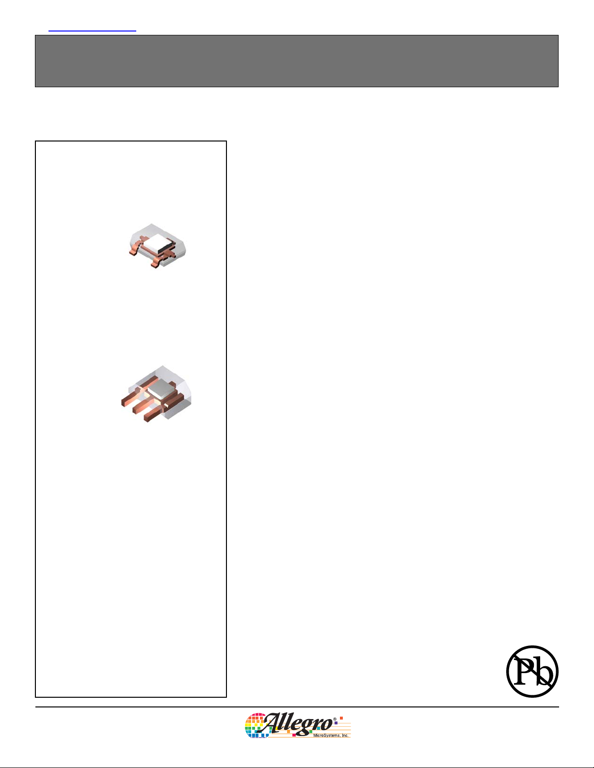
Package LH, 3-pin Surface Mount
1. VCC
2. VOUT
3. GND
Package UA, 3-pin SIP
1. VCC
2. GND
3. VOUT
1
2
1
2
3
A1301 and A1302
The A1301 and A1302 are continuous-time, ratiometric, linear Hall-effect sensors.
They are optimized to accurately provide a voltage output that is proportional to
an applied magnetic field. These devices have a quiescent output voltage that is
50% of the supply voltage. Two output sensitivity options are provided: 2.5 mV/G
typical for the A1301, and 1.3 mV/G typical for the A1302.
The Hall-effect integrated circuit included in each device includes a Hall sensing
element, a linear amplifier, and a CMOS Class A output structure. Integrating the
3
Hall sensing element and the amplifier on a single chip minimizes many of the
problems normally associated with low voltage level analog signals.
High precision in output levels is obtained by internal gain and offset trim adjustments made at end-of-line during the manufacturing process.
These features make the A1301 and A1302 ideal for use in position sensing
systems, for both linear target motion and rotational target motion. They are wellsuited for industrial applications over extended temperature ranges, from –40°C to
125°C.
Two device package types are available: LH, a 3-pin SOT23W type for surface
mount, and UA, a 3-pin ultramini SIP for through-hole mount. Each package is
available in a lead (Pb) free version (suffix, –T) with 100% matte tin plated leadframe.
AB SO LUTE MAX I MUM RAT INGS
Supply Voltage, VCC............................................8 V
Output Voltage, V
Reverse-Supply Voltage, V
Reverse-Output Voltage, V
Output Sink Current, I
Operating Temperature
Ambient, T
Ambient, T
Maximum Junction, T
Storage Temperature, T
A1301-DS, Rev. 2
.......................................... 8 V
OUT
OUT
, Range E..................–40ºC to 85ºC
A
, Range K ...............–40ºC to 125ºC
A
.......................–0.1 V
RCC
.....................–0.1 V
ROUT
............................. 10 mA
........................165ºC
J(max)
.................. –65ºC to 170ºC
S
Features and Benefits
Low-noise output
Fast power-on time
Ratiometric rail-to-rail output
4.5 to 6.0 V operation
Solid-state reliability
Factory-programmed at end-of-line for optimum performance
Robust ESD performance
Allegro MicroSystems, Inc.
115 Northeast Cutoff, Box 15036
Worcester, Massachusetts 01615-0036 (508) 853-5000
www.allegromicro.com
Page 2
A1301 and A1302
Continuous-Time Ratiometric Linear Hall Effect Sensors
Product Selection Guide
Part Number Pb-free Packing* Package
A1301ELHLT –
A1301ELHLT-T Yes
A1301EUA –
A1301EUA-T Yes
A1301KLHLT –
A1301KLHLT-T Yes
A1301KUA –
A1301KUA-T Yes
A1302ELHLT –
A1302ELHLT-T Yes
A1302EUA –
A1302EUA-T Yes
A1302KLHLT –
A1302KLHLT-T Yes
A1302KUA –
A1302KUA-T Yes
7-in. tape and reel, 3000 pieces/reel Surface Mount
Bulk, 500 pieces/bag SIP
7-in. tape and reel, 3000 pieces/reel Surface Mount
Bulk, 500 pieces/bag SIP
7-in. tape and reel, 3000 pieces/reel Surface Mount
Bulk, 500 pieces/bag SIP
7-in. tape and reel, 3000 pieces/reel Surface Mount
Bulk, 500 pieces/bag SIP
*Contact Allegro for additional packing options.
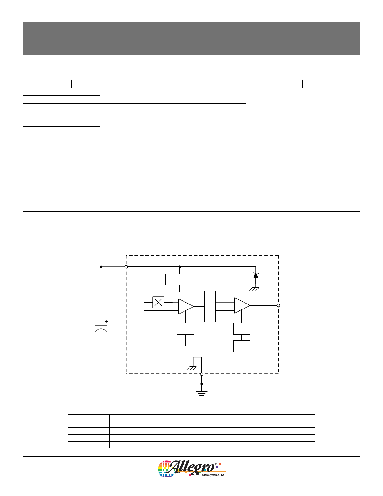
Functional Block Diagram
V+
VCC
Ambient, T
A
–40ºC to 85ºC
–40ºC to 125ºC
–40ºC to 85ºC
–40ºC to 125ºC
Sensitivity (Typical)
2.5 mV/G
1.3 mV/G
Voltage
Regulator
Out
Offset
Trim
Control
C
BYPASS
Amp
Gain
Filter
GND
Terminal List
Symbol Description
Package LH Package UA
Number
VCC Connects power supply to chip 1 1
VOUT Output from circuit 2 3
GND Ground 3 2
VOUT
A1301-DS, Rev. 2
Allegro MicroSystems, Inc.
115 Northeast Cutoff, Box 15036
Worcester, Massachusetts 01615-0036 (508) 853-5000
www.allegromicro.com
2
Page 3
A1301 and A1302
Continuous-Time Ratiometric Linear Hall Effect Sensors
DEVICE CHARACTERISTICS over operating temperature range, T
, and VCC = 5 V, unless otherwise noted
A
Characteristic Symbol Test Conditions Min. Typ. Max. Units
Electrical Characteristics
Supply Voltage V
Supply Current I
V
Output Voltage
OUT(High)ISOURCE
V
OUT(Low)ISINK
CC
CC
Running, TJ < 165°C 4.5 – 6 V
Output open – – 11 mA
= –1 mA, Sens = nominal 4.65 4.7 – V
= 1 mA, Sens = nominal – 0.2 0.25 V
Output Bandwidth BW – 20 – kHz
Power-On Time t
Output Resistance R
Wide Band Output Noise, rms V
PO
OUT
OUTN
V
Slew rate = 4.5 V/µs to 4.5 V/100 ns
I
External output low pass filter ≤ 10 kHz;
Sens = nominal
CC(min)
SINK
to 0.95 V
≤ 1 mA, I
OUT;
SOURCE
B = ±1400 G;
–35µs
≥ –1 mA – 2 5 Ω
– 150 – µV
Ratiometry
Quiescent Output Voltage Error
with respect to ∆V
CC
1
Magnetic Sensitivity Error with
respect to ∆V
CC
2
∆V
OUTQ(V)TA
∆Sens
(V)TA
= 25°C – – ±3.0 %
= 25°C – – ±3.0 %
Output
Linearity Lin TA = 25°C – – ±2.5 %
Symmetry Sym TA = 25°C – – ±3.0 %
Magnetic Characteristics
Quiescent Output Voltage V
Quiescent Output Voltage over
Operating Temperature Range
OUTQ
V
OUTQ(∆TA)
Magnetic Sensitivity Sens
Magnetic Sensitivity over
Operating Temperature Range
1
Refer to equation (4) in Ratiometric section on page 4.
2
Refer to equation (5) in Ratiometric section on page 4.
Sens
B = 0 G; TA = 25°C 2.4 2.5 2.6 V
B = 0 G 2.2 – 2.8 V
A1301; T
A1302; T
= 25°C 2.0 2.5 3.0 mV/G
A
= 25°C 1.0 1.3 1.6 mV/G
A
A1301 1.8 – 3.2 mV/G
(∆TA)
A1302 0.85 – 1.75 mV/G
A1301-DS, Rev. 2
Allegro MicroSystems, Inc.
115 Northeast Cutoff, Box 15036
Worcester, Massachusetts 01615-0036 (508) 853-5000
www.allegromicro.com
3
Page 4

A1301 and A1302
V
CC
5V
∆V
OUTQ(VCC)
∆V
OUTQ(5V)
∆V
OUTQ(∆V)
=
× 100%
V
CC
5V
=
× 100%
∆Sens
(∆V)
Sens
(VCC)
Sens
(5V)
=
× 100%
Lin+
2 (V
OUT(+B½)
–V
VOUTQ
)
–
V
OUT(+B)VOUTQ
=
× 100%
Lin–
2(V
OUT(–B½)–VOUTQ
)
–
V
OUT(–B)VOUTQ
–
=
× 100%
Sym
V
OUT(+B)
V
OUTQ–VOUT(–B)
V
OUTQ
Continuous-Time Ratiometric Linear Hall Effect Sensors
Characteristic Definitions
Quiescent Output Voltage. In the quiescent state (no sig-
nificant magnetic field: B = 0), the output, V
, equals one
OUTQ
half of the supply voltage, VCC, throughout the entire operating
ranges of VCC and ambient temperature, TA. Due to internal
component tolerances and thermal considerations, however,
there is a tolerance on the quiescent output voltage, ∆V
OUTQ
,
which is a function of both ∆VCC and ∆TA. For purposes of specification, the quiescent output voltage as a function of temperature, ∆V
OUTQ(∆TA)
∆V
, is defined as:
OUTQ(∆ΤΑ)
V
OUTQ(ΤΑ)VOUTQ(25ºC)
=
Sens
–
(25ºC)
(1)
where Sens is in mV/G, and the result is the device equivalent
accuracy, in gauss (G), applicable over the entire operating temperature range.
Sensitivity. The presence of a south-polarity (+B) magnetic
field, perpendicular to the branded face of the device package,
increases the output voltage, V
field applied, from V
toward the VCC rail. Conversely, the
OUTQ
, in proportion to the magnetic
OUT
application of a north polarity (–B) magnetic field, in the same
orientation, proportionally decreases the output voltage from its
quiescent value. This proportionality is specified as the magnetic
sensitivity of the device and is defined as:
(2)
Sens
V
OUT(–B)VOUT(+B)
=
–
2B
The stability of the device magnetic sensitivity as a function of
ambient temperature, ∆ Sens
Sens
∆Sens
(∆ΤΑ)
(ΤΑ)
=
(%) is defined as:
( ∆TA)
Sens
–
Sens
(25ºC)
(25ºC)
× 100%
(3)
Ratiometric. The A1301 and A1302 feature a ratiometric
output. This means that the quiescent voltage output, V
OUTQ
,
and the magnetic sensitivity, Sens, are proportional to the supply
voltage, VCC.
The ratiometric change (%) in the quiescent voltage output is
defined as:
(4)
and the ratiometric change (%) in sensitivity is defined as:
(5)
Linearity and Symmetry. The on-chip output stage is
designed to provide linear output at a supply voltage of 5 V.
Although the application of very high magnetic fields does not
damage these devices, it does force their output into a nonlinear
region. Linearity in percent is measured and defined as:
(6)
(7)
and output symmetry as:
(8)
A1301-DS, Rev. 2
Allegro MicroSystems, Inc.
115 Northeast Cutoff, Box 15036
Worcester, Massachusetts 01615-0036 (508) 853-5000
www.allegromicro.com
4
Page 5

A1301 and A1302
2.40
2.45
2.50
2.55
2.60
–50 –25 0 25 50 75 100 125 150
2.40
2.45
2.50
2.55
2.60
–50 –25 0 25 50 75 100 125 150
4.5 5.0 5.5 6.0
4.5 5.0 5.5 6.0
Continuous-Time Ratiometric Linear Hall Effect Sensors
Typical Characteristics
(30 pieces, 3 fabrication lots)
1301 Dev ice Sensitivity vs. Ambient Tem perature 1302 Dev ice Sensitivity vs. Temperature
2.65
2.60
2.55
2.50
2.45
Sensitivity (mV/G)
2.40
2.35
–50
–25 0 25 50 75 100 125 150
UA Package
LH Package
Temperature (°C)
1.40
1.38
1.36
1.34
1.32
1.30
Sensitivity (mV/G)
1.28
1.26
1.24
-50
-25 0 25 50 75 100 125 150
UA Package
LH Package
Temperature (°C)
Output Voltage (V)
Sensitivity (mV/G)
3.5
3.0
2.5
2.0
1.5
1301 Dev ice V
1301 Dev ice Sensitivity v s. Supply Voltage
vs. Ambient Temperature 1302 Dev ice V
OUTQ
Temperature (°C)
Supply Voltage (V)
Output Voltage (V)
Sensitivity (mV/G)
1.7
1.6
1.5
1.4
1.3
1.2
1.1
1.0
vs. Ambient Temperature
OUTQ
Temperature (°C)
1302 Dev ice Sensitivity v s. Supply Voltage
Supply Voltage (V)
Continued on the next page...
A1301-DS, Rev. 2
Allegro MicroSystems, Inc.
115 Northeast Cutoff, Box 15036
Worcester, Massachusetts 01615-0036 (508) 853-5000
www.allegromicro.com
5
Page 6

A1301 and A1302
Continuous-Time Ratiometric Linear Hall Effect Sensors
Typical Characteristics, continued
(30 pieces, 3 fabrication lots)
1301 Dev ice V
3.5
3.0
2.5
Output Voltage (V)
2.0
1.5
4.5 5.0 5.5 6.0
Supply Voltage (V)
1301 Dev ice LIN+ and LIN– vs. Supply V oltage
100.4
100.3
100.2
100.1
100.0
Linearity (%)
99.9
vs. Supply Voltage
OUTQ
LIN–
LIN+
1302 Dev ice V
3.5
3.0
2.5
Output Voltage (V)
2.0
1.5
4.5 5.0 5.5 6.0
Supply Voltage (V)
1302 Dev ice LIN+ and LIN– vs. Supply V oltage
100.0
99.9
99.8
Linearity (%)
99.7
vs. Supply Voltage
OUTQ
LIN+
LIN–
99.8
4.5
100.0
99.9
99.8
99.7
99.6
99.5
99.4
99.3
Symmetry (%)
99.2
99.1
99.0
4.5 5.0 5.5 6.0
A1301-DS, Rev. 2
5.0 5.5 6.0
Supply Voltage (V)
1301 Dev ice Symmetry v s. Supply Voltage
Supply Voltage (V)
99.6
4.5
1302 Dev ice Symmetry v s. Supply Voltage
100.5
100.4
100.3
100.2
100.1
100.0
99.9
99.8
Symmetry (%)
99.7
99.6
99.5
4.5 5.0 5.5 6.0
5.0 5.5 6.0
Supply Voltage (V)
Supply Voltage (V)
Allegro MicroSystems, Inc.
115 Northeast Cutoff, Box 15036
Worcester, Massachusetts 01615-0036 (508) 853-5000
www.allegromicro.com
6
Page 7

3.00
2.70
.118
.106
2.10
1.85
.083
.073
0.50 .020
0.30
0.55
REF
A1301 and A1302
Continuous-Time Ratiometric Linear Hall Effect Sensors
Package LH, 3-Pin; (SOT-23W)
3.10
.122
2.90
.114
1.49
0.96
NOM
.022
.038
.012
.059
3
NOM
0.28
.011
NOM
A
21
1.13
0.87
0.95
BSC
.037
0.15
0.00
.006
.000
.045
.034
8º
0º
0.20
0.13
0.25
MIN
0.25
.010
BSC
Seating Plane
Gauge Plane
.008
.005
.010
1.00
BSC
.039
0.70
BSC
Dimensions in millimeters
U.S. Customary dimensions (in.) in brackets, for reference only
A
Hall element
B
Active Area Depth 0.28 [.011]
C
Fits SC–59A Solder Pad Layout
.028
C
2.40
.094
BSC
0.95
.037
BSC
.122
.117
3.10
2.97
.640
.600
Package UA, 3-Pin; (TO-92)
.164
4.17
.159
4.04
45°
BSC
.0805
16.26
15.24
.0565
NOM
.085
MAX
2.04
NOM
1.44
B
2.16
A
231
.019
0.48
.014
0.36
Dimensions in inches
Metric dimensions (mm) in brackets, for reference only
A
Dambar removal protrusion
B
Hall element
.050
BSC
.062
.058
1.27
.031
REF
.017
.014
1.57
1.47
0.79
0.44
0.35
.0195
NOM
0.50
45°
BSC
A1301-DS, Rev. 2
Allegro MicroSystems, Inc.
115 Northeast Cutoff, Box 15036
Worcester, Massachusetts 01615-0036 (508) 853-5000
www.allegromicro.com
7
Page 8

A1301 and A1302
Continuous-Time Ratiometric Linear Hall Effect Sensors
A1301-DS, Rev. 2
The products described herein are manufactured under one or more of
the following U.S. patents: 5,045,920; 5,264,783; 5,442,283; 5,389,889;
5,581,179; 5,517,112; 5,619,137; 5,621,319; 5,650,719; 5,686,894;
5,694,038; 5,729,130; 5,917,320; and other patents pending.
Allegro MicroSystems, Inc. reserves the right to make, from time to
time, such de par tures from the detail spec i fi ca tions as may be required
to permit improvements in the per for mance, reliability, or manufacturability of its products. Before placing an order, the user is cautioned to
verify that the information being relied upon is current.
Allegro products are not authorized for use as critical components in
life-support devices or sys tems without express written approval.
The in for ma tion in clud ed herein is believed to be ac cu rate and reliable.
How ev er, Allegro MicroSystems, Inc. assumes no re spon si bil i ty for its
use; nor for any in fringe ment of patents or other rights of third parties
which may result from its use.
Copyright © 2005, Allegro MicroSystems, Inc.
Allegro MicroSystems, Inc.
115 Northeast Cutoff, Box 15036
Worcester, Massachusetts 01615-0036 (508) 853-5000
www.allegromicro.com
8
 Loading...