

Page 1
TL/F/6611
9602/DM9602 Dual Retriggerable, Resettable One Shots
June 1989
9602/DM9602 Dual Retriggerable,
Resettable One Shots
General Description
These dual resettable, retriggerable one shots have two inputs per function; one which is active high, and one which is
active low. This allows the designer to employ either leading-edge or trailing-edge triggering, which is independent of
input transition times. When input conditions for triggering
are met, a new cycle starts and the external capacitor is
allowed to rapidly discharge and then charge again. The
retriggerable feature permits output pulse widths to be extended. In fact a continuous true output can be maintained
by having an input cycle time which is shorter than the output cycle time. The output pulse may then be terminated at
any time by applying a low logic level to the RESET pin.
Retriggering may be inhibited by either connecting the Q
output to an active high input, or the Q
output to an active
low input.
Features
Y
70 ns to%output width range
Y
Resettable and retriggerableÐ0% to 100% duty cycle
Y
TTL input gatingÐleading or trailing edge triggering
Y
Complementary TTL outputs
Y
Optional retrigger lock-out capability
Y
Pulse width compensated for VCCand temperature
variations
Y
Alternate Military/Aerospace device (54xxx) is available.
Contact a National Semiconductor Sales Office/Distributor for specifications.
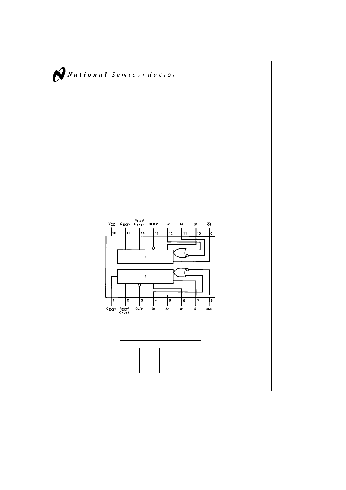
Connection Diagram
Dual-In-Line Package
TL/F/6611– 1
Order Number 9602DMQB, 9602FMQB or DM9602N
See NS Package Number J16A, N16E or W16A
Function Table
Pin No’s.
Operation
A B CLR
HxL L H Trigger
HL
x
H H Trigger
X X L Reset
HeHigh Voltage Level
L
e
Low Voltage Level
X
e
Don’t Care
C
1995 National Semiconductor Corporation RRD-B30M105/Printed in U. S. A.
Page 2
Absolute Maximum Ratings (Note)
If Military/Aerospace specified devices are required,
please contact the National Semiconductor Sales
Office/Distributors for availability and specifications.
Supply Voltage 7V
Input Voltage 5.5V
Operating Free Air Temperature Range
Military
b
55§Ctoa125§C
Commercial 0
§
Ctoa70§C
Storage Temperature Range
b
65§Ctoa150§C
Note:
The ‘‘Absolute Maximum Ratings’’ are those values
beyond which the safety of the device cannot be guaranteed. The device should not be operated at these limits. The
parametric values defined in the ‘‘Electrical Characteristics’’
table are not guaranteed at the absolute maximum ratings.
The ‘‘Recommended Operating Conditions’’ table will define
the conditions for actual device operation.
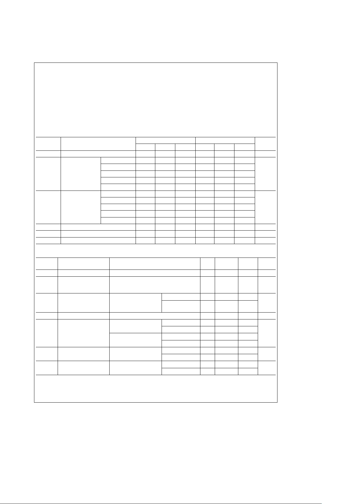
Recommended Operating Conditions
Symbol Parameter
Military Commercial
Units
Min Nom Max Min Nom Max
V
CC
Supply Voltage 4.5 5 5.5 4.75 5 5.25 V
V
IH
High Level Input T
A
eb
55§C2
Voltage
T
A
e
0§C 1.9
T
A
e
25§C 1.7 1.8 V
T
A
e
75§C 1.65
T
A
e
125§C 1.5
V
IL
Low Level Input T
A
eb
55§C 0.85
Voltage
T
A
e
0§C 0.85
T
A
e
25§C 0.9 0.85 V
T
A
e
75§C 0.85
T
A
e
125§C 0.85
I
OH
High Level Output Current
b
0.8
b
0.8 mA
I
OL
Low Level Output Current 16 16 mA
T
A
Free Air Operating Temperature
b
55 125 0 75
§
C
Electrical Characteristics over recommended operating free air temperature range (unless otherwise noted)
Symbol Parameter Conditions (Note 3) Min
Typ
Max Units
(Note 1)
V
I
Input Clamp Voltage V
CC
e
Min, I
I
eb
12 mA
b
1.5 V
V
OH
High Level Output V
CC
e
Min, I
OH
e
Max
Voltage V
IL
e
Max, V
IH
e
Min 2.4 V
(Note 4)
V
OL
Low Level Output V
CC
e
Min, I
OL
e
Max MIL 0.4
Voltage V
IL
e
Max, V
IH
e
Min
COM
0.45
V
(Note 4)
I
IH
High Level Input Current V
CC
e
Max, V
I
e
4.5V 60 mA
I
IL
Low Level Input V
CC
e
Max MIL V
I
e
0.40V
b
1.6
Current
COM V
I
e
0.45V
b
1.6
mA
V
CC
e
Min MIL V
I
e
0.40V
b
1.24
COM V
I
e
0.45V
b
1.41
I
OS
Short Circuit V
CC
e
Max, V
OUT
e
1V MIL
b
25
mA
Output Current (Notes 2 and 4)
COM
b
35
I
CC
Supply Current V
CC
e
Max MIL 39 45
mA
COM 39 50
Note 1: All typicals are at V
CC
e
5V, T
A
e
25§C.
Note 2: Not more than one output should be shorted at a time.
Note 3: Unless otherwise noted, R
X
e
10k for all tests.
Note 4: Ground PIN 1(15) for V
OL
on PIN 7(9) or VOHand IOSon PIN 6(10) and apply momentary ground to PIN 4(12). Open PIN 1(15) for VOLon PIN 6(10) or V
OH
and IOSon PIN 7(9).
2
Page 3
Switching Characteristics V
CC
e
5V, T
A
e
25§C (See Section 1 for Test Waveforms and Output Load)
Symbol Parameter Conditions
Military Commercial
Units
Min Max Min Max
t
PLH
Propagation Delay Time, Negative Trigger Input
35 40 ns
Low-to-High Level Output to True Output
t
PHL
Propagation Delay Time, Negative Trigger Input
C
L
e
15 pF
43 48 ns
High-to-Low Level Output To Complement Output
C
X
e
0
tPW(MIN) Minimum True Output
R
X
e
5kX
90 100
Pulse Width
ns
Minimum Complement
100 110
Pulse Width
t
PW
Pulse Width R
X
e
10 kX
3.08 3.76 3.08 3.76 ms
C
X
e
1000 pF
C
STRAY
Maximum Allowable Wiring Pins 2, 14 to
50 50 pF
Capacitance GND
R
X
External Timing Resistor 5 25 5 50 kX
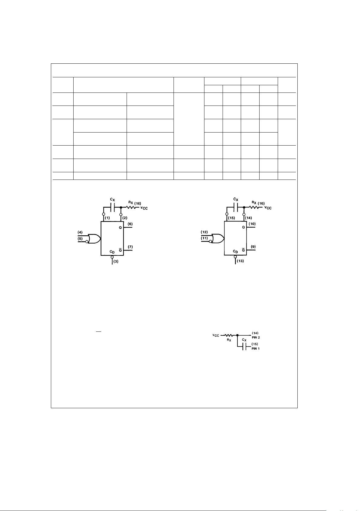
Logic Diagrams
TL/F/6611– 2
Operating Rules
TL/F/6611– 3
1. An external resistor (RX) and external capacitor (CX) are
required as shown in the Logic Diagram.
2. The value of C
X
may vary from 0 to any necessary value
available. If, however, the capacitor has leakages approaching 3.0 mA or if stray capacitance from either terminal to ground is more than 50 pF, the timing equations
may not represent the pulse width obtained.
3. The output pulse with (t) is defined as follows:
t
e
KRXC
X
Ð
1
a
1
R
X
(
for C
X
l
103pF
K&0.34
where: R
X
is in kX,CXis in pF
tisinns
for C
X
k
103pF, see
Figure 1.
forKvsCXsee
Figure 6.
4. If electrolytic type capacitors are to be used, the following
three configurations are recommended:
A. Use with low leakage capacitors:
The normal RC configuration can be used predictably
only if the forward capacitor leakage at 5.0V is less
than 3 mA, and the inverse capacitor leakage at 1.0V is
less than 5 mA over the operational temperature
range.
Rk0.6 RX(Max) TL/F/6611– 4
3
Page 4
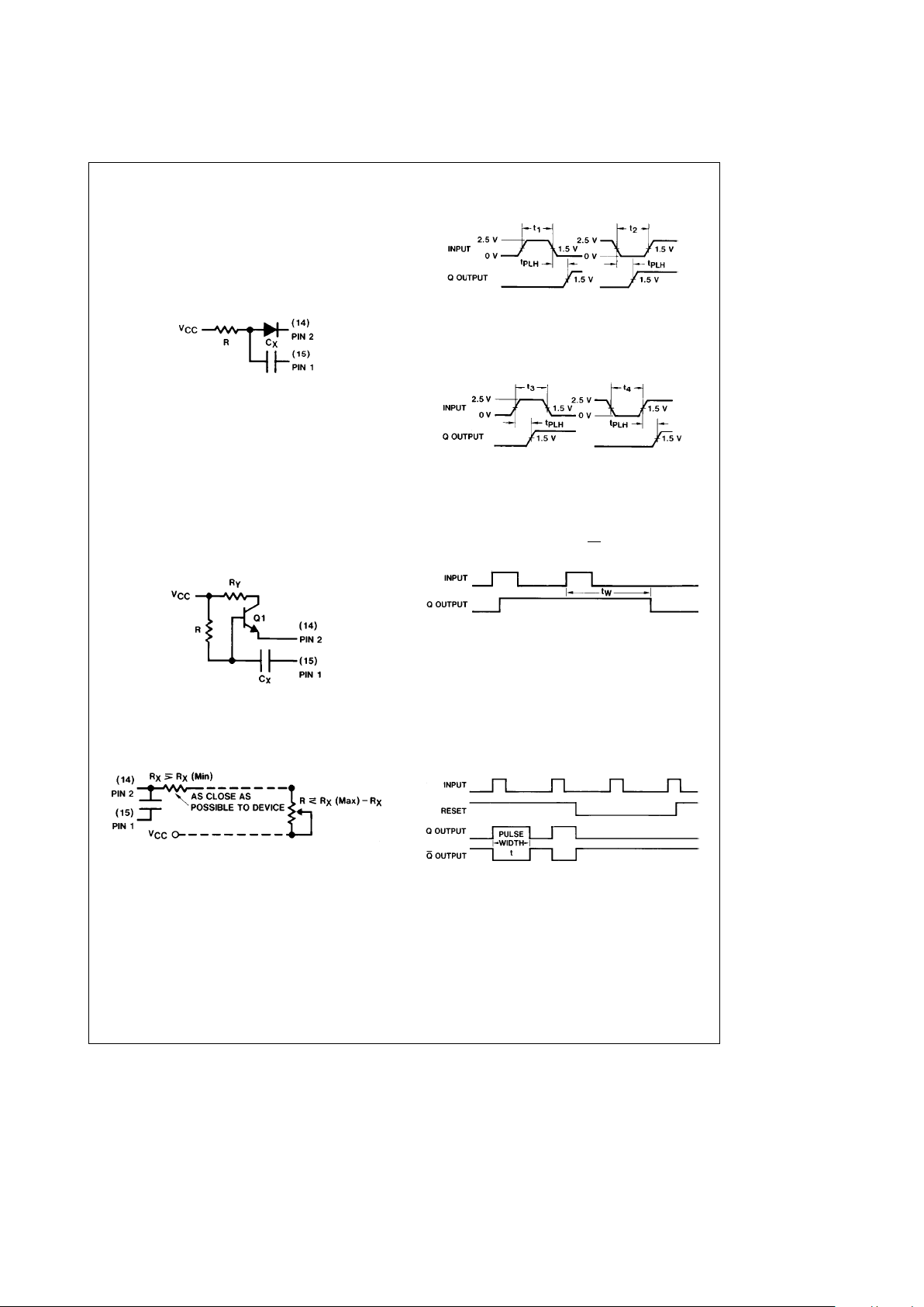
Operating Rules (Continued)
B. Use with high inverse leakage current electrolytic ca-
pacitors:
The diode in this configuration prevents high inverse
leakage currents through the capacitor by preventing
an inverse voltage across the capacitor. The use of
this configuration is not recommended with retriggerable operation.
t&0.3 RC
X
TL/F/6611– 5
C. Use to obtain extended pulse widths:
This configuration can be used to obtain extended
pulse widths, because of the larger timing resistor allowed by beta multiplication. Electrolytics with high inverse leakage currents can be used.
R
k
RX(0.7) (hFEQ1) ork2.5 MX, whichever is the
lesser
R
X
(min)kR
Y
k
RX(max)
(5 kXsR
Y
s
10 kX is recommended)
Q1: NPN silicon transistor with hFErequirements of
above equations, such as 2N5961 or 2N5962.
t&0.3 RC
X
TL/F/6611– 6
This configuration is not recommended with retriggerable operation.
5. To obtain variable pulse width by remote trimming, the
following circuit is recommended:
TL/F/6611– 7
6. Under any operating condition, CXand RX(min) must be
kept as close to the circuit as possible to minimize stray
capacitance and reduce noise pickup.
7. Input Trigger Pulse Rules (See Triggering Truth Table)
TL/F/6611– 8
Input to Pin 5(11), (Pin 3(13)eHIGH)
Pin 4(12)eLOW
t1,t
3
e
Min. Positive Input Pulse Widthl40 ns
t2,t
4
e
Min. Negative Input Pulse Widthl40 ns
TL/F/6611– 9
Input to Pin 4(12) (Pin 3(13)eHIGH)
Pin 5(11)eHIGH
8. The retriggerable pulse width is calculated as shown below:
t
W
eta
t
PLH
e
KRXC
X
#
1
a
1
R
X
J
a
t
PLH
TL/F/6611– 10
The retrigger pulse width is equal to the pulse width (t) plus a delay time. For
pulse widths greater than 500 ns, t
W
can be approximated as t. Retriggering will
not occur if the retrigger pulse comes within&0.3 C
X
(ns) after the initial trigger
pulse (i.e., during the discharge cycle).
9. Reset OperationÐAn overriding clear (active LOW level)
is provided on each one shot. By applying a LOW to the
reset, any timing cycle can be terminated or any new cycle inhibited until the LOW reset input is removed. Trigger
inputs will not produce spikes in the output when the reset is held LOW.
TL/F/6611– 11
10. VCCand Ground wiring should conform to good high
frequency standards so that switching transients on V
CC
and Ground leads do not cause interaction between one
shots. Use of a 0.01 to 0.1 mF bypass capacitor between V
CC
and Ground located near the DM9602 is rec-
ommended.
*For further detailed device characteristics and output performance, please
refer to the NSC one-shot application note, AN-366.
4
Page 5
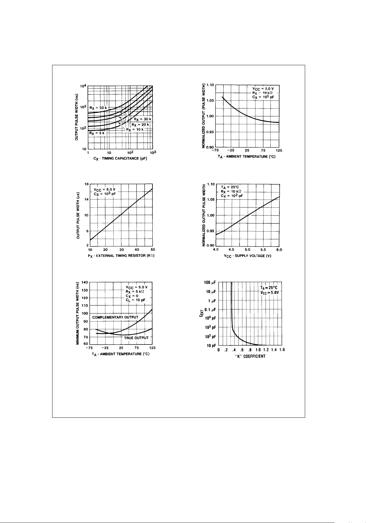
Typical Performance Characteristics
TL/F/6611– 12
FIGURE 1. Output Pulse Width vs Timing Resistance
and Capacitance for C
X
k
103pF
TL/F/6611– 13
FIGURE 2. Normalized Output Pulse Width
vs Ambient Temperature
TL/F/6611– 14
FIGURE 3. Pulse Width vs Timing Resistor
TL/F/6611– 15
FIGURE 4. Normalized Output Pulse Width
vs Supply Voltage
TL/F/6611– 16
FIGURE 5. Minimum Output Pulse Width
vs Ambient Temperature
TL/F/6611– 17
FIGURE 6. Typical ‘‘K’’ Coefficient Variation
vs Timing Capacitance
5
Page 6

6
Page 7
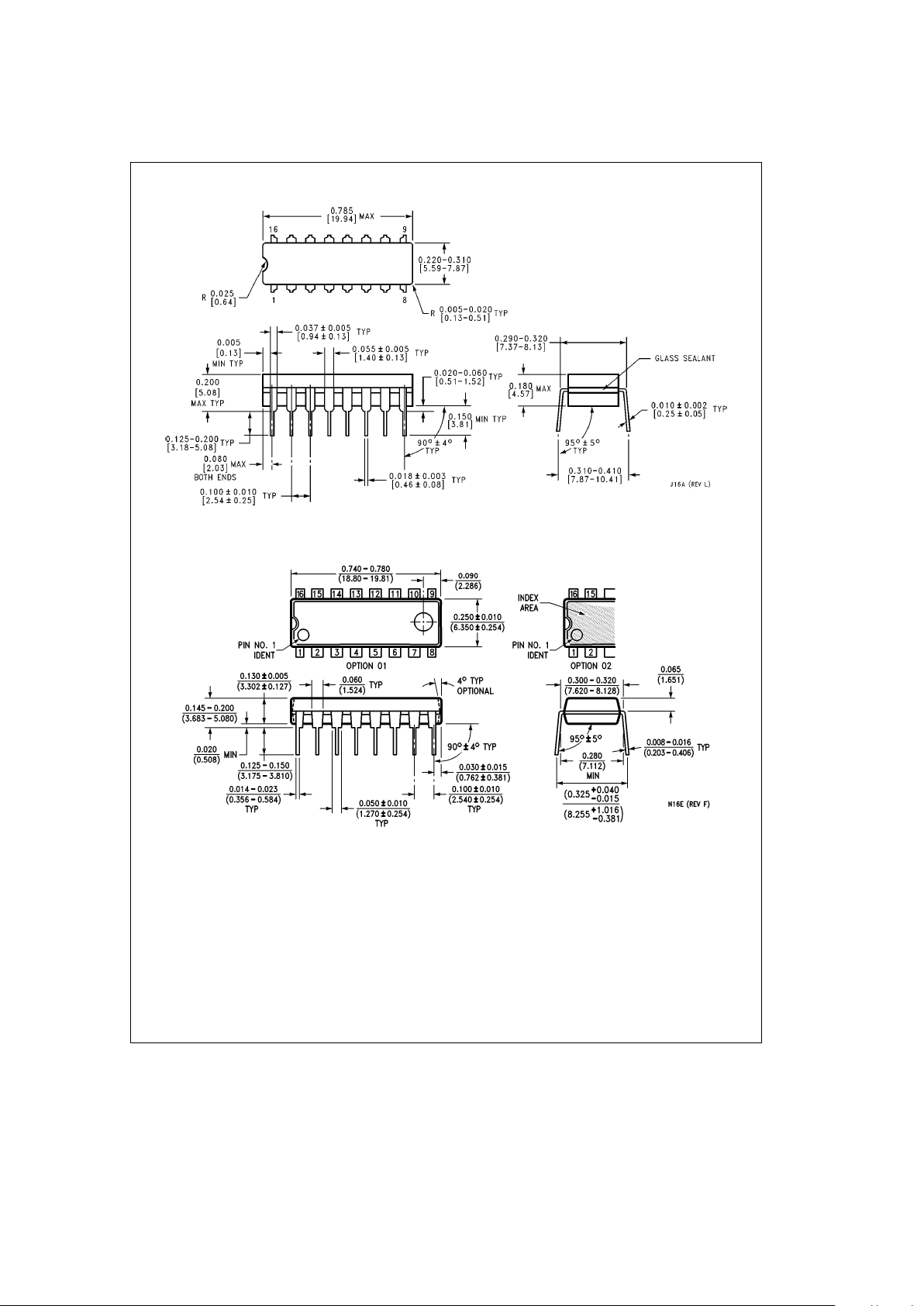
Physical Dimensions inches (millimeters)
16-Lead Ceramic Dual-In-Line Package (J)
Order Number 9602DMQB
NS Package Number J16A
16-Lead Molded Dual-In-Line Package (N)
Order Number DM9602N
NS Package Number N16E
7
Page 8
9602/DM9602 Dual Retriggerable, Resettable One Shots
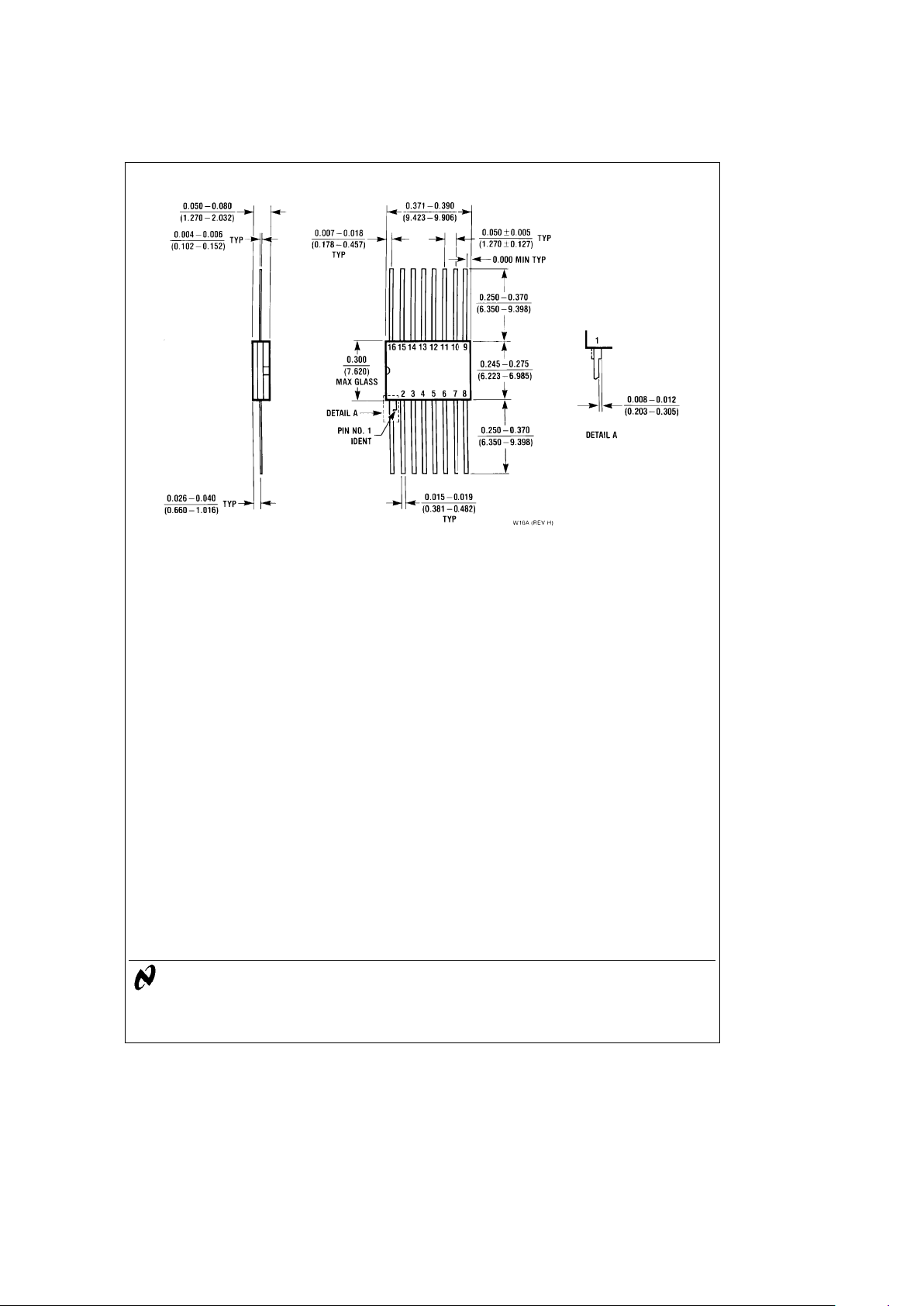
Physical Dimensions inches (millimeters) (Continued)
16-Lead Ceramic Flat Package (W)
Order Number 9602FMQB
NS Package Number W16A
LIFE SUPPORT POLICY
NATIONAL’S PRODUCTS ARE NOT AUTHORIZED FOR USE AS CRITICAL COMPONENTS IN LIFE SUPPORT
DEVICES OR SYSTEMS WITHOUT THE EXPRESS WRITTEN APPROVAL OF THE PRESIDENT OF NATIONAL
SEMICONDUCTOR CORPORATION. As used herein:
1. Life support devices or systems are devices or 2. A critical component is any component of a life
systems which, (a) are intended for surgical implant support device or system whose failure to perform can
into the body, or (b) support or sustain life, and whose be reasonably expected to cause the failure of the life
failure to perform, when properly used in accordance support device or system, or to affect its safety or
with instructions for use provided in the labeling, can effectiveness.
be reasonably expected to result in a significant injury
to the user.
National Semiconductor National Semiconductor National Semiconductor National Semiconductor
Corporation Europe Hong Kong Ltd. Japan Ltd.
1111 West Bardin Road Fax: (
a
49) 0-180-530 85 86 13th Floor, Straight Block, Tel: 81-043-299-2309
Arlington, TX 76017 Email: [email protected] Ocean Centre, 5 Canton Rd. Fax: 81-043-299-2408
Tel: 1(800) 272-9959 Deutsch Tel: (
a
49) 0-180-530 85 85 Tsimshatsui, Kowloon
Fax: 1(800) 737-7018 English Tel: (
a
49) 0-180-532 78 32 Hong Kong
Fran3ais Tel: (
a
49) 0-180-532 93 58 Tel: (852) 2737-1600
Italiano Tel: (
a
49) 0-180-534 16 80 Fax: (852) 2736-9960
National does not assume any responsibility for use of any circuitry described, no circuit patent licenses are implied and National reserves the right at any time without notice to change said circuitry and specifications.
 Loading...