

Page 1
93L28
Dual 8-Bit Shift Register
93L28 Dual 8-Bit Shift Register
June 1989
General Description
The 93L28 is a high speed serial storage element providing
16 bits of storage in the form of two 8-bit registers. The
multifunctional capability of this device is provided by several features: 1) additional gating is provided at the input to
both shift registers so that the input is easily multiplexed
between two sources; 2) the clock of each register may be
provided separately or together; 3) both the true and complementary outputs are provided from each 8-bit register,
and both registers may be master cleared from a common
input.
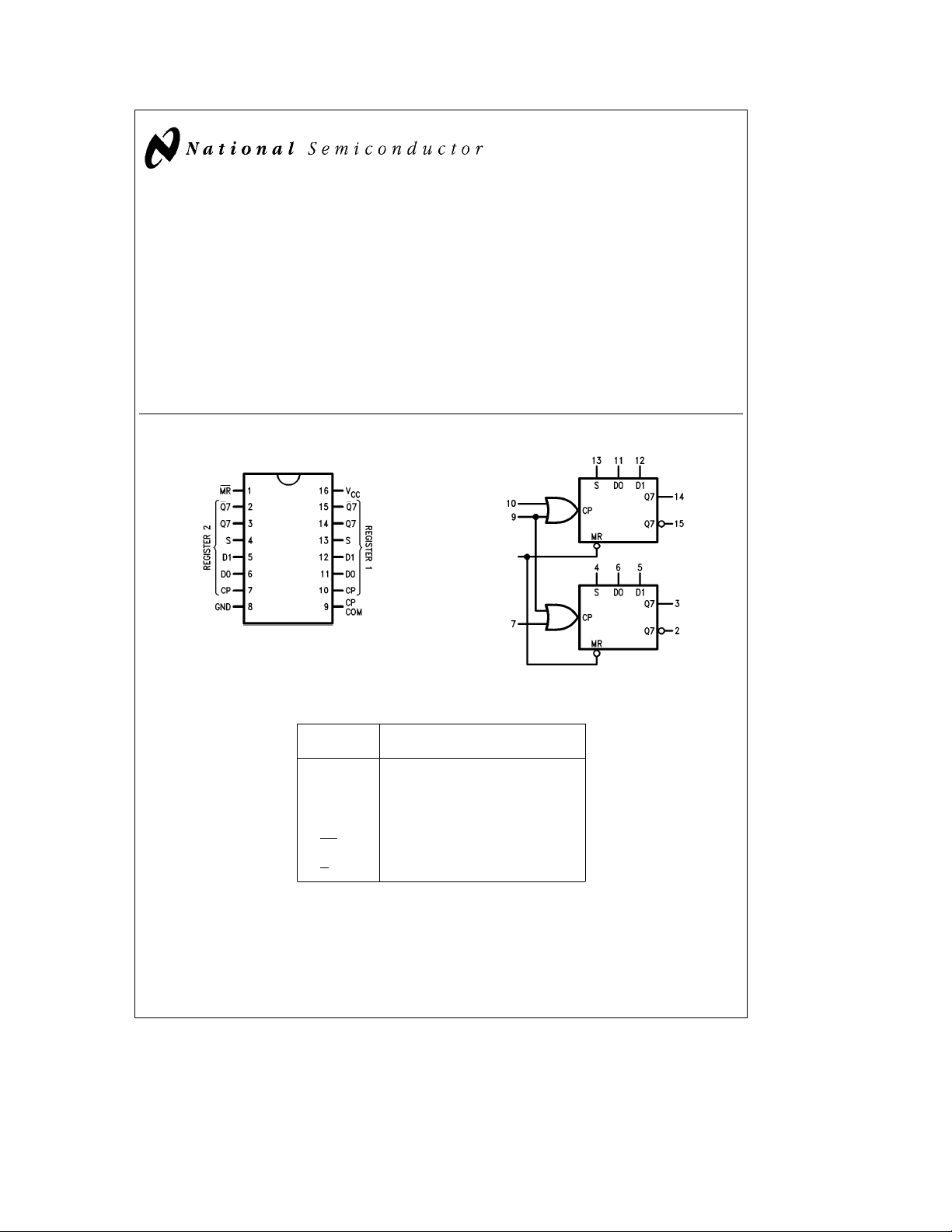
Connection Diagram
Dual-In-Line Package
TL/F/10200– 1
Order Number 93L28DMQB or 93L28FMQB
See NS Package Number J16A or W16A
Features
Y
2-input multiplexer provided at data input of each
register
Y
Gated clock input circuitry
Y
Both true and complementary outputs provided from
last bit of each register
Y
Asynchronous master reset common to both registers
Logic Symbol
V
CC
GND
e
e
Pin 16
Pin 8
TL/F/10200– 2
Pin
Names
S Data Select Input
D0, D1 Data Inputs
CP Clock Pulse Input (Active HIGH)
MR Master Reset Input (Active LOW)
Q7 Last Stage Output
Q
7 Complementary Output
C
1995 National Semiconductor Corporation RRD-B30M105/Printed in U. S. A.
TL/F/10200
Description
Common (Pin 9)
Separate (Pins 7 and 10)
Page 2
Absolute Maximum Ratings (Note)
Note:
If Military/Aerospace specified devices are required,
please contact the National Semiconductor Sales
Office/Distributors for availability and specifications.
Supply Voltage 7V
Input Voltage 5.5V
Operating Free Air Temperature Range
MIL
Storage Temperature Range
b
55§Ctoa125§C
b
65§Ctoa150§C
The ‘‘Absolute Maximum Ratings’’ are those values
beyond which the safety of the device cannot be guaranteed. The device should not be operated at these limits. The
parametric values defined in the ‘‘Electrical Characteristics’’
table are not guaranteed at the absolute maximum ratings.
The ‘‘Recommended Operating Conditions’’ table will define
the conditions for actual device operation.
Recommended Operating Conditions
Symbol Parameter
V
CC
V
IH
V
IL
I
OH
I
OL
T
A
ts(H) Setup Time HIGH or LOW 30
t
(L) Dnto CP 30
s
th(H) Hold Time HIGH or LOW 0
th(L) Dnto CP 0
tw(H) Clock Pulse Width 55
t
(L) HIGH or LOW 55
w
tw(L) MR Pulse Width with CP HIGH 60 ns
tw(L) MR Pulse Width with CP LOW 70 ns
Supply Voltage 4.5 5 5.5 V
High Level Input Voltage 2 V
Low Level Input Voltage 0.7 V
High Level Output Current
Low Level Output Current 4.8 mA
Free Air Operating Temperature
Min Nom Max
b
55 125
93L28 (MIL)
b
400 mA
Units
C
§
ns
ns
ns
2
Page 3

Electrical Characteristics over recommended operating free air temperature (unless otherwise noted)
Symbol Parameter Conditions Min
e
e
Max, V
e
Min, V
e
e
Min, I
Min, I
Min, I
Max, V
Max, V
eb
10 mA
I
e
Max,
OH
e
Min
IH
e
Max,
OL
e
Max
IL
e
5.5V
I
e
2.4V MR,Dx 20
I
2.4 V
CP (7, 10) 30
V
I
V
OH
V
OL
I
I
I
IH
Input Clamp Voltage V
High Level Output Voltage V
Low Level Output Voltage V
Input Current@Max V
Input Voltage
HIGH Level V
Input Current
CC
CC
e
V
IL
CC
e
V
IH
CC
CC
S40
CP Com 60
I
IL
LOW Level V
Input Current
CC
e
Max, V
e
0.3V MR,Dx
I
CP (7, 10)
S
CP Com
I
OS
I
CC
Note 1: All typicals are at V
Note 2: Not more than one output should be shorted at a time, and the duration should not exceed one second.
Switching Characteristics
V
CC
Short Circuit V
Output Current (Note 2)
Supply Current V
e
e
5V, T
CC
A
ea
5.0V, T
ea
25§C (See Section 1 for test waveforms and output load)
A
25§C.
Symbol Parameter
e
Max
CC
e
Max 25.3 mA
CC
b
e
15 pF
C
L
Min Max
f
t
t
t
max
PLH
PHL
PHL
Maximum Shift Right Frequency 5.0 MHz
Propagation Delay 45
CP to Q7or Q
Propagation Delay MR to Q
7
7
2.5
Typ
(Note 1)
Max Units
b
0.3 V
b
400
b
600
b
800
b
1200
b
80
110 ns
1.5 V
1mA
mA
mA
25 mA
Units
ns
3
Page 4

Functional Description
The two 8-bit shift registers have a common clock input (pin
9) and separate clock inputs (pins 10 and 7). The clocking
of each register is controlled by the OR function of the separate and the common clock input. Each register is composed of eight clocked RS master/slave flip-flops and a
number of gates. The clock OR gate drives the eight clock
inputs of the flip-flops in parallel. When the two clock inputs
(the separate and the common) to the OR gate are LOW,
the slave latches are steady, but data can enter the master
latches via the R and S input. During the first LOW-to-HIGH
transition of either, or both simultaneously, of the two clock
inputs, the data inputs (R and S) are inhibited so that a later
change in input data will not affect the master; then the now
trapped information in the master is transferred to the slave.
When the transfer is complete, both the master and the
slave are steady as long as either or both clock inputs remain HIGH. During the HIGH-to-LOW transition of the last
remaining HIGH clock input, the transfer path from master
to slave is inhibited first, leaving the slave steady in its present state. The data inputs (R and S) are enabled so that new
data can enter the master. Either of the clock inputs can be
used as clock inhibit inputs by applying a logic HIGH signal.
Logic Diagram
Each 8-bit shift register has a 2-input multiplexer in front of
the serial data input. The two data inputs D0 and D1 are
controlled by the data select input (S) following the Boolean
expression:
Serial data in: S
e
D
SD0aSD1
An asynchronous master reset is provided which, when activated by a LOW logic level, will clear all 16 stages independently of any other input signal.
Shift Select Table
Inputs Output
SD0D1Q7(t
)
a
n
8
LL X L
LH X H
HX L L
HX H H
e
H
HIGH Voltage Level
e
LOW Voltage Level
L
e
Immaterial
X
a8e
Indicates state after eight clock pulse
n
TL/F/10200– 3
4
Page 5

Physical Dimensions inches (millimeters)
16-Lead Ceramic Dual-In-Line Package (J)
Order Number 93L28DMQB
NS Package Number J16A
5
Page 6

Physical Dimensions inches (millimeters) (Continued)
93L28 Dual 8-Bit Shift Register
16-Lead Ceramic Flat Package (W)
Order Number 93L28FMQB
NS Package Number W16A
LIFE SUPPORT POLICY
NATIONAL’S PRODUCTS ARE NOT AUTHORIZED FOR USE AS CRITICAL COMPONENTS IN LIFE SUPPORT
DEVICES OR SYSTEMS WITHOUT THE EXPRESS WRITTEN APPROVAL OF THE PRESIDENT OF NATIONAL
SEMICONDUCTOR CORPORATION. As used herein:
1. Life support devices or systems are devices or 2. A critical component is any component of a life
systems which, (a) are intended for surgical implant support device or system whose failure to perform can
into the body, or (b) support or sustain life, and whose be reasonably expected to cause the failure of the life
failure to perform, when properly used in accordance support device or system, or to affect its safety or
with instructions for use provided in the labeling, can effectiveness.
be reasonably expected to result in a significant injury
to the user.
National Semiconductor National Semiconductor National Semiconductor National Semiconductor
Corporation Europe Hong Kong Ltd. Japan Ltd.
1111 West Bardin Road Fax: (
Arlington, TX 76017 Email: cnjwge@tevm2.nsc.com Ocean Centre, 5 Canton Rd. Fax: 81-043-299-2408
Tel: 1(800) 272-9959 Deutsch Tel: (
Fax: 1(800) 737-7018 English Tel: (
National does not assume any responsibility for use of any circuitry described, no circuit patent licenses are implied and National reserves the right at any time without notice to change said circuitry and specifications.
Fran3ais Tel: (
Italiano Tel: (
a
49) 0-180-530 85 86 13th Floor, Straight Block, Tel: 81-043-299-2309
a
49) 0-180-530 85 85 Tsimshatsui, Kowloon
a
49) 0-180-532 78 32 Hong Kong
a
49) 0-180-532 93 58 Tel: (852) 2737-1600
a
49) 0-180-534 16 80 Fax: (852) 2736-9960
 Loading...