

Page 1
93L24
5-Bit Comparator
93L24 5-Bit Comparator
June 1989
General Description
The 93L24 expandable comparator provides comparison
between two 5-bit words and gives three outputsБ‘less
than’’, ‘‘greater than’’ and ‘‘equal to’’. A HIGH on the active
LOW Enable Input forces all three outputs LOW.
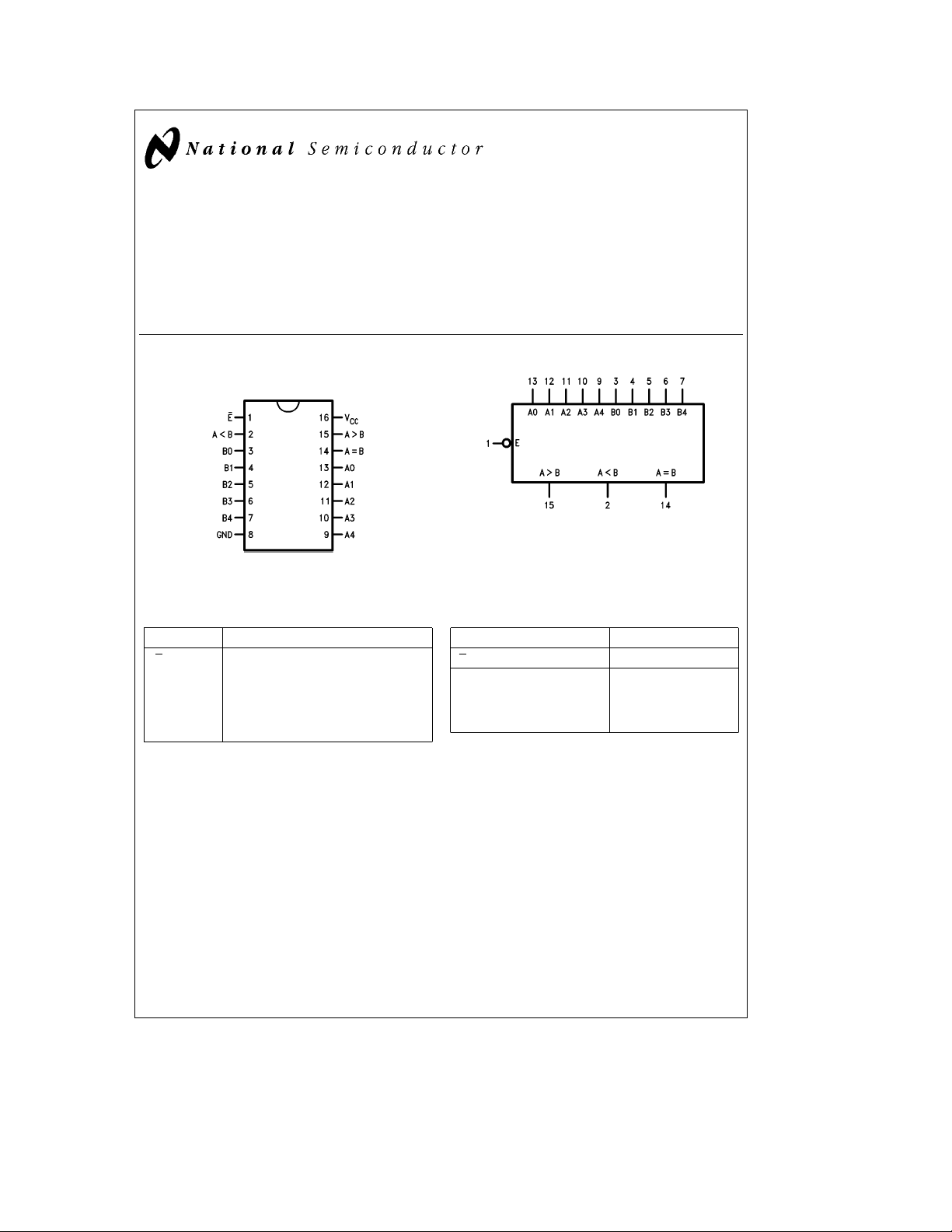
Connection Diagram
Dual-In-Line Package
Order Number 93L24DMQB or 93L24FMQB
See NS Package Number J16A or W16A
Pin Names Description
E Enable Input (Active LOW)
A0–A4 Word A Parallel Inputs
B0–B4 Word B Parallel Inputs
k
A
B A Less than B Output (Active HIGH)
l
A
B A Greater than B Output (Active HIGH)
e
A
B A Equal to B Output (Active HIGH)
TL/F/10199– 1
Features
Y
Three separate outputs: AkB, AlB, AeB
Y
Easily expandable
Y
Active low enable input
Logic Symbol
V
CC
GND
e
Pin 16
e
Pin 8
TL/F/10199– 2
Truth Table
Inputs Outputs
E An Bn AkBAlBAeB
HX X LLL
L Word A
L Word A
L Word B
HeHIGH Voltage Level
e
LOW Voltage Level
L
e
Immaterial
X
e
Word B L L H
l
Word B L H L
k
Word A H L L
C
1995 National Semiconductor Corporation RRD-B30M105/Printed in U. S. A.
TL/F/10199
Page 2
Absolute Maximum Ratings (Note)
Note:
If Military/Aerospace specified devices are required,
please contact the National Semiconductor Sales
Office/Distributors for availability and specifications.
Supply Voltage 7V
Input Voltage 5.5V
Operating Free Air Temperature Range
MIL
Storage Temperature Range
b
55§Ctoa125§C
b
65§Ctoa150§C
The ‘‘Absolute Maximum Ratings’’ are those values
beyond which the safety of the device cannot be guaranteed. The device should not be operated at these limits. The
parametric values defined in the ‘‘Electrical Characteristics’’
table are not guaranteed at the absolute maximum ratings.
The ‘‘Recommended Operating Conditions’’ table will define
the conditions for actual device operation.
Recommended Operating Conditions
Symbol Parameter
V
CC
V
IH
V
IL
I
OH
I
OL
T
A
Supply Voltage 4.5 5 5.5 V
High Level Input Voltage 2 V
Low Level Input Voltage 0.7 V
High Level Output Current
Low Level Output Current 4.8 mA
Free Air Operating Temperature
Min Nom Max
b
55 125
93L24 (MIL)
b
400 mA
Electrical Characteristics over recommended operating free air temperature (unless otherwise noted)
Symbol Parameter Conditions Min
e
V
I
V
OH
V
OL
I
I
I
IH
I
IL
I
OS
I
CC
Note 1: All typicals are at V
Note 2: Not more than one output should be shorted at a time, and the duration should not exceed one second.
Input Clamp Voltage V
High Level Output Voltage V
Low Level Output Voltage V
Input Current@Max V
Input Voltage
High Level Input Current V
Low Level Input Current V
Short Circuit V
Output Current
Supply Current V
e
e
5V, T
CC
25§C.
A
CC
CC
e
V
IL
CC
e
V
IH
CC
CC
CC
CC
CC
eb
Min, I
e
Min, I
Max, V
e
Min, I
Min, V
e
Max, V
e
Max, V
e
Max, V
e
Max (Note 2)
e
Max 21 mA
10 mA
I
e
Max,
OH
e
Min
IH
e
Max,
OL
e
Max
IL
e
5.5V
I
e
2.4V 40 mA
I
e
0.3V
I
2.4 V
b
2.5
Typ
(Note 1)
Max Units
b
1.5 V
0.3 V
1mA
b
0.8 mA
b
25 mA
Units
C
§
2
Page 3

Switching Characteristics
ea
V
CC
5.0V, T
ea
25§C (See Section 1 for test waveforms and output load)
A
Symbol Parameter
t
PLH
t
PHL
t
PLH
t
PHL
t
PLH
t
PHL
t
PLH
t
PHL
Propagation Delay 32
E to AeB; E to AkB, AlB35
Propagation Delay 54
An to AlB; Bn to AlB75
Propagation Delay 70
An to AkB; Bn to AkB77
Propagation Delay 100
An or Bn to AeB 102
e
15 pF
C
L
Min Max
Units
ns
ns
ns
ns
Functional Description
The 93L24 5-bit comparators use combinational circuitry to
directly generate ‘‘A greater than B’’ and ‘‘A less than B’’
outputs. As evident from the logic diagram, these ouptuts
are generated in only three gate delays. The ‘‘A equals B’’
output is generated in one additional gate delay by decoding
the ‘‘A neither less than nor greater than B’’ condition with a
NOR gate. All three outputs are activated by the active LOW
Enable Input (E
).
Logic Diagram
Tying the A
another device and the A
l
B output from one device into an A input on
k
B output into the corresponding
B input permits easy expansion.
The A4 and B4 inputs are the most significant inputs and
A0, B0 the least significant. Thus if A4 is HIGH and B4 is
LOW, the A
inputs except E
l
B output will be HIGH regardless of all other
.
TL/F/10199– 3
3
Page 4

Physical Dimensions inches (millimeters)
93L24 5-Bit Comparator
16-Lead Ceramic Dual-In-Line Package (J)
Order Number 93L24DMQB
NS Package Number J16A
16-Lead Ceramic Flat Package (W)
Order Number 93L24FMQB
NS Package Number W16A
LIFE SUPPORT POLICY
NATIONAL’S PRODUCTS ARE NOT AUTHORIZED FOR USE AS CRITICAL COMPONENTS IN LIFE SUPPORT
DEVICES OR SYSTEMS WITHOUT THE EXPRESS WRITTEN APPROVAL OF THE PRESIDENT OF NATIONAL
SEMICONDUCTOR CORPORATION. As used herein:
1. Life support devices or systems are devices or 2. A critical component is any component of a life
systems which, (a) are intended for surgical implant support device or system whose failure to perform can
into the body, or (b) support or sustain life, and whose be reasonably expected to cause the failure of the life
failure to perform, when properly used in accordance support device or system, or to affect its safety or
with instructions for use provided in the labeling, can effectiveness.
be reasonably expected to result in a significant injury
to the user.
National Semiconductor National Semiconductor National Semiconductor National Semiconductor
Corporation Europe Hong Kong Ltd. Japan Ltd.
1111 West Bardin Road Fax: (
Arlington, TX 76017 Email: cnjwge@tevm2.nsc.com Ocean Centre, 5 Canton Rd. Fax: 81-043-299-2408
Tel: 1(800) 272-9959 Deutsch Tel: (
Fax: 1(800) 737-7018 English Tel: (
National does not assume any responsibility for use of any circuitry described, no circuit patent licenses are implied and National reserves the right at any time without notice to change said circuitry and specifications.
Fran3ais Tel: (
Italiano Tel: (
a
49) 0-180-530 85 86 13th Floor, Straight Block, Tel: 81-043-299-2309
a
49) 0-180-530 85 85 Tsimshatsui, Kowloon
a
49) 0-180-532 78 32 Hong Kong
a
49) 0-180-532 93 58 Tel: (852) 2737-1600
a
49) 0-180-534 16 80 Fax: (852) 2736-9960
 Loading...