

Page 1
93L00
4-Bit Universal Shift Register
93L00 4-Bit Universal Shift Register
June 1989
General Description
The 93L00 is a 4-bit universal shift register. As a high speed
multifunctional sequential logic block, it is useful in a wide
variety of register and counter applications. It may be used
in serial-serial, shift left, shift right, serial-parallel, parallelserial, and parallel-parallel data register transfers.
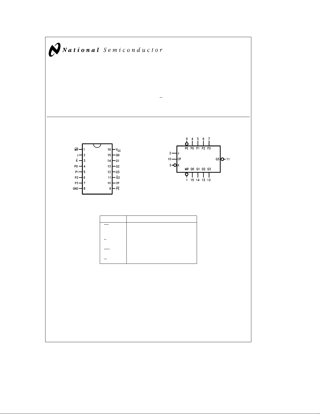
Connection Diagram
Dual-In-Line Package
Order Number 93L00DMQB or 93L00FMQB
See NS Package Number J16A or W16A
Pin Names Description
PE Parallel Enable Input (Active LOW)
P0–P3 Parallel Inputs
J First Stage J Input (Active HIGH)
K
CP Clock Pulse Input (Active Rising Edge)
MR
Q0–Q3 Parallel Outputs
Q
3 Complementary Last Stage Output
TL/F/9576– 1
First Stage K Input (Active LOW)
Master Reset Input
Features
Y
Asynchronous master reset
Y
J, K inputs to first stage
Logic Symbol
V
CC
GND
e
e
Pin 16
Pin 8
TL/F/9576– 2
C
1995 National Semiconductor Corporation RRD-B30M105/Printed in U. S. A.
TL/F/9576
Page 2
Absolute Maximum Ratings (Note)
Note:
If Military/Aerospace specified devices are required,
please contact the National Semiconductor Sales
Office/Distributors for availability and specifications.
Supply Voltage 7V
Input Voltage 5.5V
Operating Free Air Temperature Range
MIL
b
65§Ctoa125§C
The ‘‘Absolute Maximum Ratings’’ are those values
beyond which the safety of the device cannot be guaranteed. The device should not be operated at these limits. The
parametric values defined in the ‘‘Electrical Characteristics’’
table are not guaranteed at the absolute maximum ratings.
The ‘‘Recommended Operating Conditions’’ table will define
the conditions for actual device operation.
Recommended Operating Conditions
Symbol Parameter
Min Nom Max
V
CC
V
IH
V
IL
I
OH
I
OL
T
A
Supply Voltage 4.5 5 5.5 V
High Level Input Voltage 2 V
Low Level Input Voltage 0.7 V
High Level Output Voltage
Low Level Output Current 4.8 mA
Free Air Operating Temperature
b
55 125
ts(H) Setup Time HIGH or LOW, 60
t
(L) J, K and P0 – P3 to CP 60
s
th(H) Hold Time HIGH or LOW, 0
th(L) J, K and P0 –P3 to CP 0
ts(H) Setup Time HIGH or LOW, 68
t
(L) PE to CP 68
s
th(H) Hold Time HIGH or LOW, 0
t
(L) PE to CP 0
h
tw(H) CP Pulse Width 38
t
(L) HIGH or LOW 38
w
tw(L) MR Pulse Width LOW 53 ns
t
rec
Recovery Time, MR to CP 70 ns
93L00 (MIL)
b
0.4 mA
Units
C
§
ns
ns
ns
ns
ns
2
Page 3
Electrical Characteristics
Over recommended operating free air temperature range (unless otherwise noted)
Symbol Parameter Conditions Min
e
V
I
V
OH
V
OL
I
I
I
IH
I
IL
I
OS
I
CC
Note 1: All typicals are at V
Note 2: Not more than one output should be shorted at a time, and the duration should not exceed one second.
Switching Characteristics
V
CC
Input Clamp Voltage V
High Level Output Voltage V
Low Level Output Voltage V
Input Current@Max V
Input Voltage
High Level Input Current V
Low Level Input Current V
Short Circuit V
Output Current (Note 2)
Supply Current V
e
e
5V, T
CC
A
ea
5.0V, T
ea
25§C (See Section 1 for waveforms and load configurations)
A
25§C.
CC
CC
e
V
IL
CC
e
V
IH
CC
CC
CC
CC
CC
Symbol Parameter C
f
t
t
t
max
PLH
PHL
PHL
Maximum Shift Frequency 10 MHz
Propagation Delay 35
CP to Q
n
Propagation Delay, MR to Q
eb
e
Max, V
e
Min, V
e
e
Min, I
Min, I
Min, I
Max, V
Max, V
10 mA
I
e
Max,
OH
e
Min
IH
e
Max,
OL
e
Max
IL
e
5.5V
I
e
2.4V Inputs 20
I
2.4 3.4 V
CP 40 mA
PE 46
e
Max, V
e
0.3V Inputs
I
CP
PE
e
Max
e
Max 23 mA
b
93L
e
L
Min Max
n
Typ
(Note 1)
Max Units
b
1.5 V
0.3 V
1mA
b
400
b
800 mA
b
920
2.5
b
25 mA
15 pF Units
51
ns
60 ns
3
Page 4

Functional Description
The Logic Diagrams and Truth Table indicate the functional
characteristics of the 93L00 4-bit shift register. The device is
useful in a wide variety of shifting, counting and storage
applications. It performs serial, parallel, serial-to-parallel, or
parallel-to-serial data transfers.
The 93L00 has two primary modes of operation, shift right
(Q0
x
Q1) and parallel load, which are controlled by the
state of the Parallel Enable (PE
) input. When the PE input is
HIGH, serial data enters the first flip-flop Q0 via the J and K
inputs and is shifted one bit in the direction
Q0
xQ1xQ2x
clock transition. The JK
Q3 following each LOW-to-HIGH
inputs provide the flexibility of the
JK type input for special applications, and the simple D-type
input for general applications by tying the two pins together.
When the PE
input is LOW, the 93L00 appears as four common clocked D flip-flops. The data on the parallel inputs
P0–P3 is transferred to the respective Q0–Q3 outputs following the LOW-to-HIGH clock transition. Shift left operation (Q3
x
Q2) can be achieved by tying the Qn outputs to
b
the Pn
1 inputs and holding the PE input LOW.
All serial and parallel data transfers are synchronous, occuring after each LOW-to-HIGH clock transition. Since the
93L00 utilizes edge triggering, there is no restriction on the
activity of the J, K
, Pn and PE inputs for logic operationÐexcept for the setup and release time requirements. A LOW on
the asynchronous Master Reset (MR
) input sets all Q out-
puts LOW, independent of any other input condition.
Truth Table
Operating Inputs (MReH) Outputs@t
Mode
PE JKP0 P1 P2 P3 Q0 Q1 Q2 Q3 Q3
H L L X X X X L Q0 Q1 Q2 Q2
Shift Mode
H LH X X X X Q0Q0Q1Q2Q
HHLXXXXQ
0Q0Q1Q2Q2
H H H X X X X H Q0 Q1 Q2 Q
Parallel L X X L L L L L L L L H
Entry Mode L X X H H H H H H H H L
e
*t
Indicates state after next LOW-to-HIGH clock transition.
na1
e
HIGH Voltage Level
H
e
LOW Voltage Level
L
e
Immaterial
X
na1
2
2
4
Page 5

Logic Diagram
TL/F/9576– 3
5
Page 6

6
Page 7

Physical Dimensions inches (millimeters)
16-Lead Ceramic Dual-In-Line Package (J)
Order Number 93L00DMQB
NS Package Number J16A
7
Page 8

Physical Dimensions inches (millimeters) (Continued)
93L00 4-Bit Universal Shift Register
16-Lead Ceramic Flat Package (W)
Order Number 93L00FMQB
NS Package Number W16A
LIFE SUPPORT POLICY
NATIONAL’S PRODUCTS ARE NOT AUTHORIZED FOR USE AS CRITICAL COMPONENTS IN LIFE SUPPORT
DEVICES OR SYSTEMS WITHOUT THE EXPRESS WRITTEN APPROVAL OF THE PRESIDENT OF NATIONAL
SEMICONDUCTOR CORPORATION. As used herein:
1. Life support devices or systems are devices or 2. A critical component is any component of a life
systems which, (a) are intended for surgical implant support device or system whose failure to perform can
into the body, or (b) support or sustain life, and whose be reasonably expected to cause the failure of the life
failure to perform, when properly used in accordance support device or system, or to affect its safety or
with instructions for use provided in the labeling, can effectiveness.
be reasonably expected to result in a significant injury
to the user.
National Semiconductor National Semiconductor National Semiconductor National Semiconductor
Corporation Europe Hong Kong Ltd. Japan Ltd.
1111 West Bardin Road Fax: (
Arlington, TX 76017 Email: cnjwge@tevm2.nsc.com Ocean Centre, 5 Canton Rd. Fax: 81-043-299-2408
Tel: 1(800) 272-9959 Deutsch Tel: (
Fax: 1(800) 737-7018 English Tel: (
National does not assume any responsibility for use of any circuitry described, no circuit patent licenses are implied and National reserves the right at any time without notice to change said circuitry and specifications.
Fran3ais Tel: (
Italiano Tel: (
a
49) 0-180-530 85 86 13th Floor, Straight Block, Tel: 81-043-299-2309
a
49) 0-180-530 85 85 Tsimshatsui, Kowloon
a
49) 0-180-532 78 32 Hong Kong
a
49) 0-180-532 93 58 Tel: (852) 2737-1600
a
49) 0-180-534 16 80 Fax: (852) 2736-9960
 Loading...