

Page 1

6121 Baker Road,
Suite 108
Minnetonka, MN 55345
www.chtechnology.com
Phone (952) 933-6190
Fax (952) 933-6223
1-800-274-4284
Thank you for downloading this document from C&H Technology, Inc.
Please contact the C&H Technology team for the following questions -
Technical
Application
Assembly
Availability
Pricing
Phone – 1-800-274-4284
E-Mail – [email protected]
www.chtechnology.com - SPECIALISTS IN POWER ELECTRONIC COMPONENTS AND ASSEMBLIES - www.chtechnology.com
Page 2

D-PAK
PRODUCT SUMMARY
VF at 5 A 1 V
I
FSM
V
RRM
8EWS..SPbF High Voltage Series
Surface Mountable
Input Rectifier Diode, 8 A
DESCRIPTION/FEATURES
cathode
1
Anode
Base
4, 2
3
Anode
200 A
800/1200 V
The 8EWS..SPbF rectifier High Voltage Series
has been optimized for very low forward
voltage drop, with moderate leakage. The glass
passivation technology used has reliable
operation up to 150 °C junction temperature.
The high reverse voltage range available allows design of
input stage primary rectification with outstanding voltage
surge capability.
Typical applications are in input rectification and these
products are designed to be used with Vishay HPP switches
and output rectifiers which are available in identical package
outlines.
This product has been designed and qualified for industrial
level and lead (Pb)-free.
Vishay High Power Products
Available
RoHS*
COMPLIANT
OUTPUT CURRENT IN TYPICAL APPLICATIONS
APPLICATIONS SINGLE-PHASE BRIDGE THREE-PHASE BRIDGE UNITS
NEMA FR-4 or G10 glass fabric-based epoxy
with 4 oz. (140 µm) copper
Aluminum IMS, R
Aluminum IMS with heatsink, R
Note
•T
= 55 °C, TJ = 125 °C, footprint 300 mm
A
= 15 °C/W 2.5 2.8
thCA
= 5 °C/W 5.5 6.5
thCA
2
1.2 1.6
MAJOR RATINGS AND CHARACTERISTICS
SYMBOL CHARACTERISTICS VALUES UNITS
I
F(AV)
V
RRM
I
FSM
V
F
T
J
Sinusoidal waveform 8 A
800/1200 V
200 A
8 A, TJ = 25 °C 1.10 V
- 55 to 150 °C
VOLTAGE RATINGS
V
, MAXIMUM
PART NUMBER
8EWS08SPbF 800 900
8EWS12SPbF 1200 1300
RRM
PEAK REVERSE VOLTAGE
V
V
, MAXIMUM NON-REPETITIVE
RSM
PEAK REVERSE VOLTAGE
V
I
RRM
AT 150 °C
mA
0.5
A
* Pb containing terminations are not RoHS compliant, exemptions may apply
www.vishay.com
Page 3

8EWS..SPbF High Voltage Series
Vishay High Power Products
Surface Mountable
Input Rectifier Diode, 8 A
ABSOLUTE MAXIMUM RATINGS
PARAMETER SYMBOL TEST CONDITIONS VALUES UNITS
Maximum average forward current I
Maximum peak one cycle
non-repetitive surge current
Maximum I
Maximum I
2
t for fusing I2t
2
√t for fusing I2√t t = 0.1 to 10 ms, no voltage reapplied 1450 A2√s
F(AV)
I
FSM
ELECTRICAL SPECIFICATIONS
PARAMETER SYMBOL TEST CONDITIONS VALUES UNITS
Maximum forward voltage drop V
Forward slope resistance r
Threshold voltage V
Maximum reverse leakage current I
F(TO)
RM
TC = 105 °C, 180 ° conduction half sine wave 8
10 ms sine pulse, rated V
applied 170
RRM
10 ms sine pulse, no voltage reapplied 200
10 ms sine pulse, rated V
applied 130
RRM
10 ms sine pulse, no voltage reapplied 145
FM
8 A, TJ = 25 °C 1.1 V
t
TJ = 150 °C
TJ = 25 °C
T
= 150 °C 0.50
J
V
= Rated V
R
RRM
20 mΩ
0.82 V
0.05
A
A
mA
2
s
THERMAL - MECHANICAL SPECIFICATIONS
PARAMETER SYMBOL TEST CONDITIONS VALUES UNITS
Maximum junction and storage
temperature range
Soldering temperature T
Maximum thermal resistance,
junction to case
Typical thermal resistance,
junction to ambient (PCB mount)
Approximate weight
Marking device Case style D-PAK (TO-252AA) 8EWS12S
Note
(1)
When mounted on 1" square (650 mm2) PCB of FR-4 or G-10 material 4 oz. (140 µm) copper 40 °C/W
For recommended footprint and soldering techniques refer to application note #AN-994
T
, T
J
Stg
S
R
DC operation 2.5
thJC
(1)
62
R
thJA
- 55 to 150
240
1g
0.03 oz.
°C
°C/W
www.vishay.com For technical questions, contact: [email protected]
Document Number: 94349
2 Revision: 22-Jul-08
Page 4
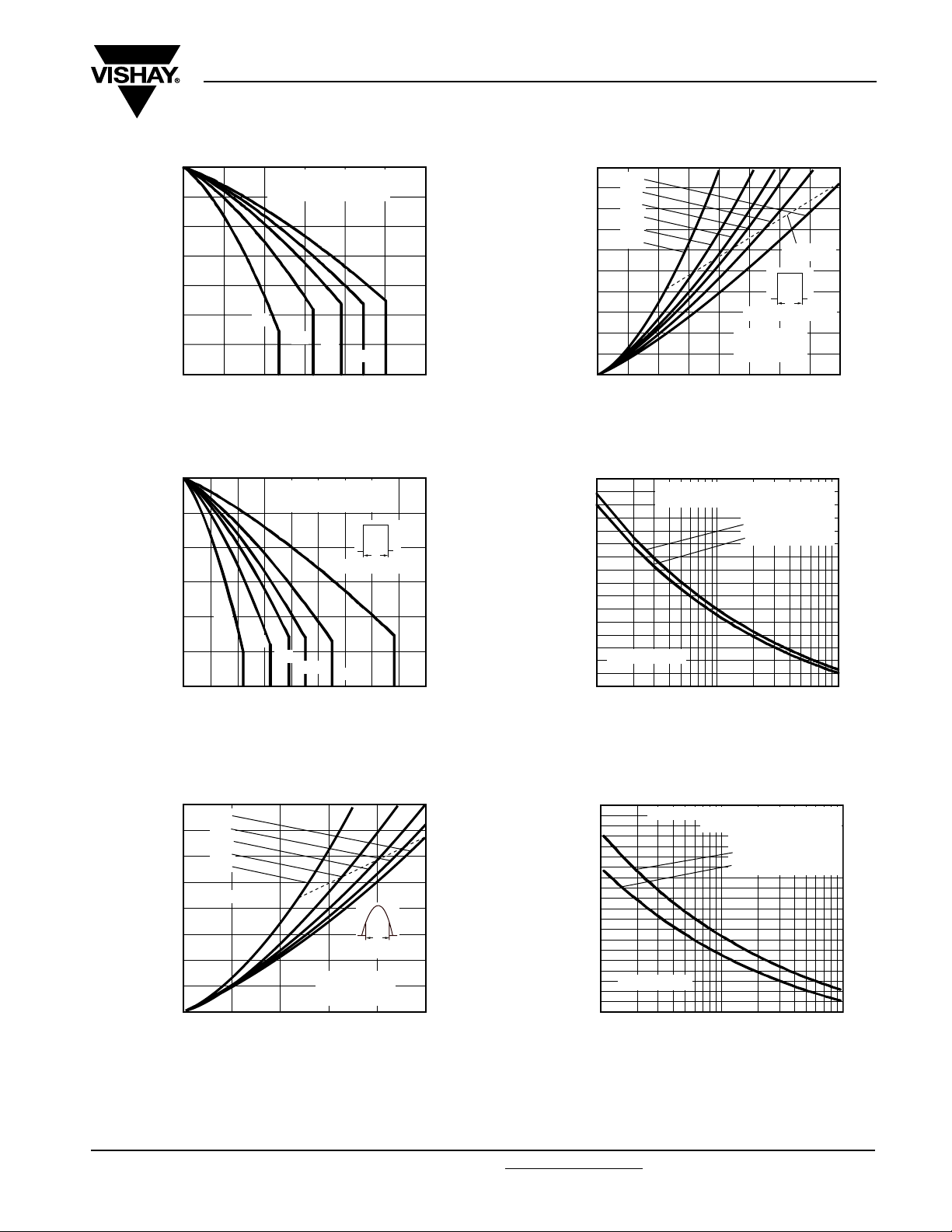
8EWS..SPbF High Voltage Series
150
140
130
120
110
100
Temperature (°C)
Maximum Allowable Case
90
80
0
30°
2
468
Average Forward Current (A)
Fig. 1 - Current Rating Characteristics
150
140
130
120
110
Temperature (°C)
100
Maximum Allowable Case
90
30°
60°
0
4268
Average Forward Current (A)
Fig. 2 - Current Rating Characteristics
8EWS. Series
R
(DC) = 2.5 °C/W
thJC
60°
90°
8EWS. Series
(DC) = 2.5 °C/W
R
thJC
90°
120°
10 12 14
Surface Mountable
Input Rectifier Diode, 8 A
120°
180°
10
12
Ø
Conduction period
180°
DC
16
18
Vishay High Power Products
20
18
16
14
12
10
Power Loss (W)
Maximum Average Forward
200
180
160
140
120
100
80
Forward Current (A)
Peak Half Sine Wave
60
40
DC
180°
120°
90°
60°
30°
8
6
4
2
0
0
246
Average Forward Current (A)
Conduction period
8EWS. Series
T
= 150 °C
J
81012
Fig. 4 - Forward Power Loss Characteristics
At any rated load condition and with
rated V
8EWS. Series
1
applied following surge.
RRM
Initial TJ = 150 °C
at 60 Hz 0.0083 s
at 50 Hz 0.0100 s
10
Number of Equal Amplitude Half
Cycle Current Pulse (N)
Fig. 5 - Maximum Non-Repetitive Surge Current
RMS limit
Ø
14
16
100
16
14
12
10
Power Loss (W)
Maximum Average Forward
180°
120°
90°
60°
30°
8
6
4
2
0
0
RMS limit
4268
Average Forward Current (A)
Fig. 3 - Forward Power Loss Characteristics
Ø
Conduction angle
8EWS. Series
T
= 150 °C
J
10
240
220
200
180
160
140
120
100
Forward Current (A)
Peak Half Sine Wave
80
60
40
0.01
Maximum non-repetitive surge current
8EWS. Series
Pulse Train Duration (s)
versus pulse train duration.
Initial TJ = 150 °C
No voltage reapplied
Rated V
0.1
Fig. 6 - Maximum Non-Repetitive Surge Current
RRM
reapplied
1
Document Number: 94349 For technical questions, contact: [email protected]
www.vishay.com
Revision: 22-Jul-08 3
Page 5
8EWS..SPbF High Voltage Series
Vishay High Power Products
100
10
Instantaneous Forward Current (A)
1
10
Surface Mountable
Input Rectifier Diode, 8 A
TJ = 25 °C
TJ = 150 °C
8EWS. Series
0
Instantaneous Forward Voltage (V)
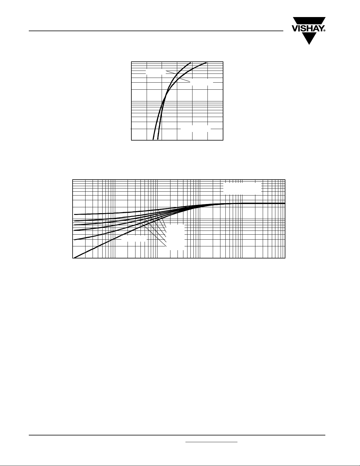
Fig. 7 - Forward Voltage Drop Characteristics
1.00.5 1.5 2.0
2.5 3.0
Steady state value
(DC operation)
1
D = 0.50
- Transient Thermal
Impedance (°C/W)
thJC
Z
0.1
0.0001 0.001 0.01 0.1 1
Single pulse
D = 0.33
D = 0.25
D = 0.17
D = 0.08
Square Wave Pulse Duration (s)
Fig. 8 - Thermal Impedance Z
Characteristics
thJC
10
Document Number: 94349
Page 6
8EWS..SPbF High Voltage Series
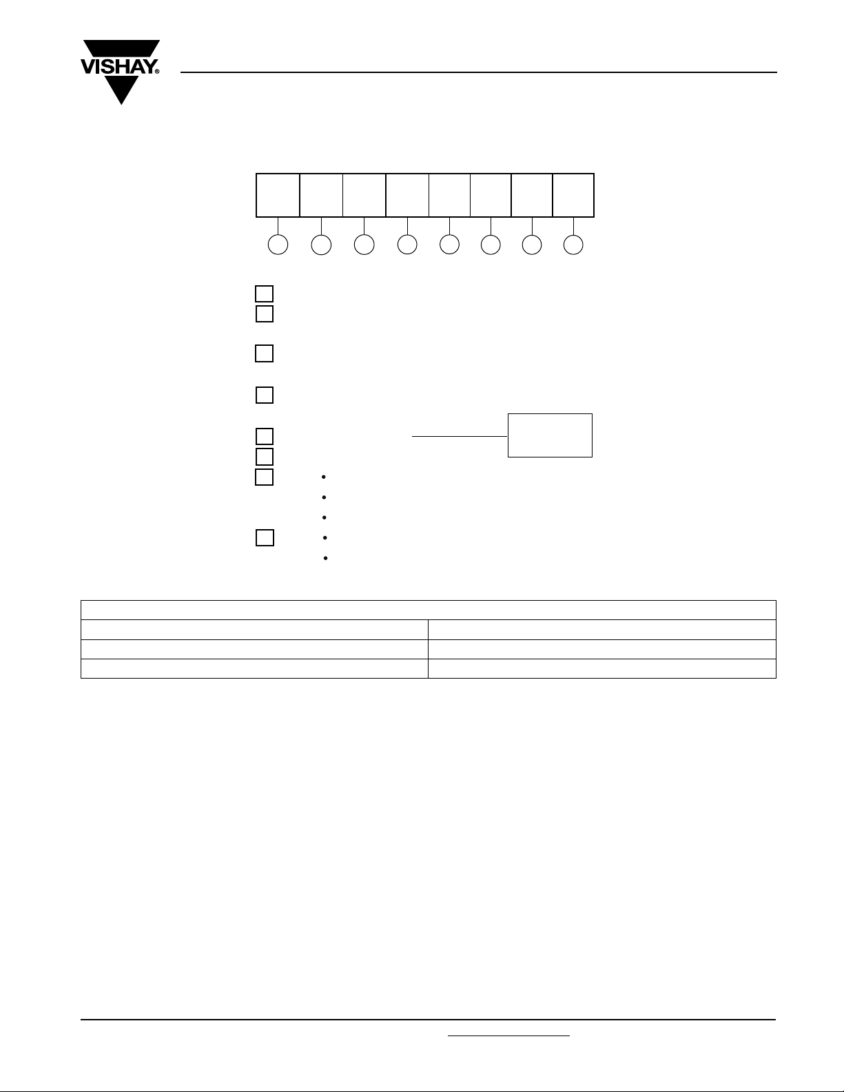
ORDERING INFORMATION TABLE
Device code
8 E W S 12 S TR PbF
1 - Current rating (8 = 8 A)
2 - Circuit configuration:
E = Single diode
3 - Package:
W = D-PAK
4 - Type of silicon:
S = Standard recovery rectifier
5 - Voltage ratings
6 -
7 -
8
S = Surface mountable
Surface Mountable
Input Rectifier Diode, 8 A
51324678
08 = 800 V
12 = 1200 V
TR = Tape and reel
TRR = Tape and reel (right oriented)
TRL = Tape and reel (left oriented)
None = Standard production
PbF = Lead (Pb)-free
Vishay High Power Products
LINKS TO RELATED DOCUMENTS
Dimensions http://www.vishay.com/doc?95016
Part marking information http://www.vishay.com/doc?95059
Packaging information http://www.vishay.com/doc?95033
www.vishay.com
Page 7

Legal Disclaimer Notice
Vishay
Notice
The products described herein were acquired by Vishay Intertechnology, Inc., as part of its acquisition of
International Rectifier’s Power Control Systems (PCS) business, which closed in April 2007. Specifications of the
products displayed herein are pending review by Vishay and are subject to the terms and conditions shown below.
Specifications of the products displayed herein are subject to change without notice. Vishay Intertechnology, Inc., or
anyone on its behalf, assumes no responsibility or liability for any errors or inaccuracies.
Information contained herein is intended to provide a product description only. No license, express or implied, by
estoppel or otherwise, to any intellectual property rights is granted by this document. Except as provided in Vishay's
terms and conditions of sale for such products, Vishay assumes no liability whatsoever, and disclaims any express
or implied warranty, relating to sale and/or use of Vishay products including liability or warranties relating to fitness
for a particular purpose, merchantability, or infringement of any patent, copyright, or other intellectual property right.
The products shown herein are not designed for use in medical, life-saving, or life-sustaining applications.
Customers using or selling these products for use in such applications do so at their own risk and agree to fully
indemnify Vishay for any damages resulting from such improper use or sale.
International Rectifier
are registered trademarks of International Rectifier Corporation in the U.S. and other countries. All other product
names noted herein may be trademarks of their respective owners.
®
, IR®, the IR logo, HEXFET®, HEXSense®, HEXDIP®, DOL®, INTERO®, and POWIRTRAIN
®
Document Number: 99901 www.vishay.com
Revision: 12-Mar-07 1
 Loading...