

Page 1
QUICK START GUIDE FOR DEMONSTRATION CIRCUIT 868
1
DESCRIPTION
LOW QUIESCENT CURRENT DUAL SYNCHRONOUS BUCK CONVERTER
LTC3827EG-1
Demonstration circuit 868 is a dual-output stepdown
power supply. The input voltage is from 4.5V to 32V.
The supply has two outputs: 3.3V/5A
8.5V/3.5A
. When the input voltage is close to the
MAX
MAX
and
output voltage, the supply is in dropout mode. The design features the LTC3827-1, the low quiescent current,
2-phase, dual-output synchronous buck regulator.
Operating the two high side MOSFETs 180 degrees out
of phase significantly reduces peak input ripple current;
thereby reducing input capacitance and EMI noise. Both
tion during short-circuit conditions. The LTC3827-1 features a precision 0.8V reference and a power good output indicator. The PLLIN/MODE pin selects among Burst
Mode operation, pulse skipping mode, or continuous
inductor current mode at light loads. The controller can
operate at up to 99% duty cycle for very low dropout
capability.
Design files for this circuit board are available. Call
the LTC factory.
, LTC and LT are registered trademarks of Linear Technology Corporation.
controllers have internal current foldback for overload
condition. Current foldback limits MOSFET heat dissipa-
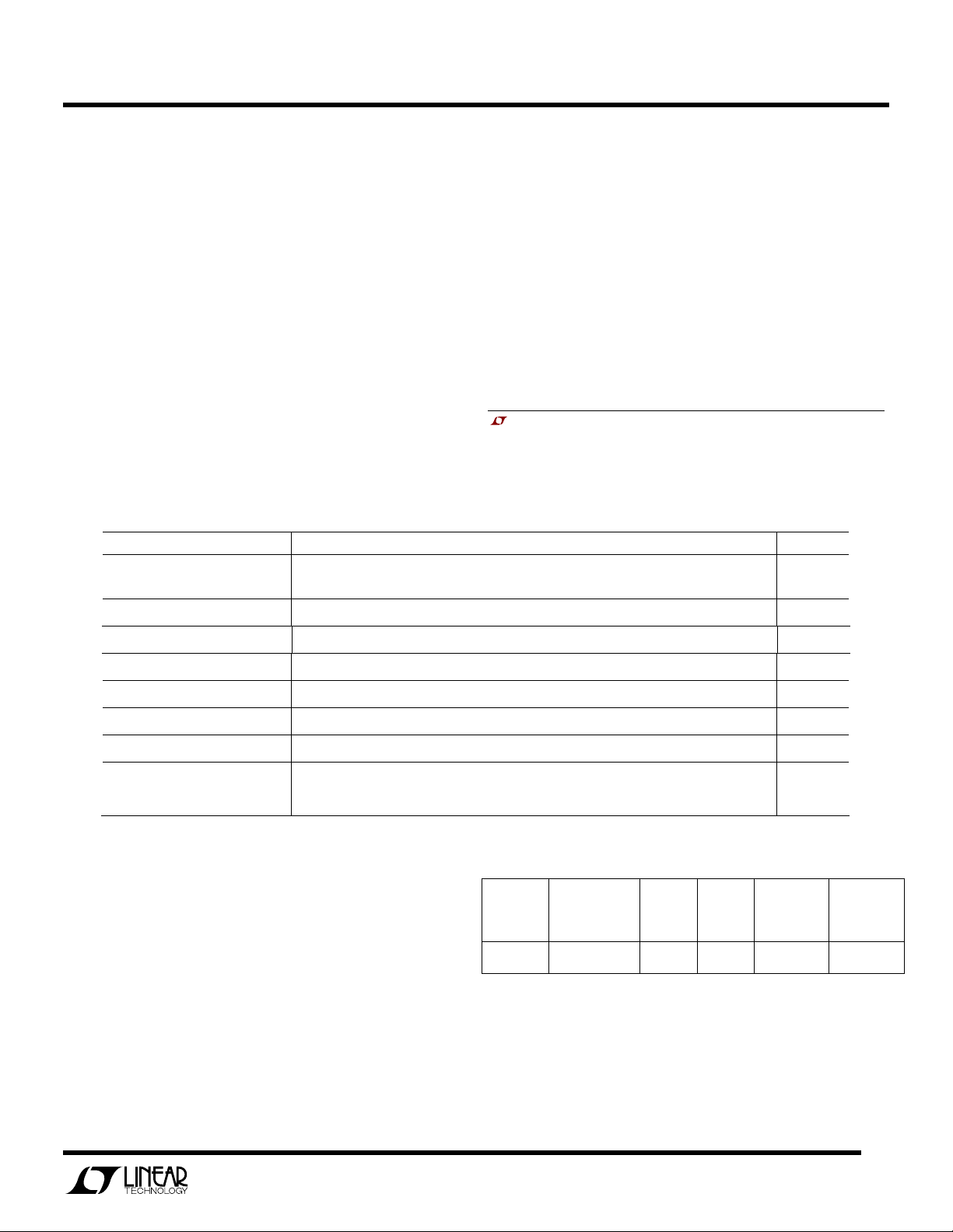
Table 1. Performance Summary
PARAMETER CONDITION VALUE
Input Voltage Range If the input voltage must exceed 32V, use higher voltage rating input capacitors. The IC
works up to 36V. Minimum of 9V input is needed for 8.5V output regulation at 3A load.
Outputs V
V
Typical Output Ripple (V
Typical Output Ripple (V
Typical Operating Frequency PLLLPF floating (position JP1 to 400Khz) 400kHz
) 20MHz BW, 5A load, VIN = 32V, frequency = 400kHz 35mV
OUT1
) 20MHz BW, 3.5A load, VIN = 32V, frequency = 400kHz 30mV
OUT2
= 3.3V, 0A to 5A 3.3V ± 2%
OUT1
= 8.5V, 0A to 3.5A, Vin>9V 8.5V ± 2%
OUT2
4.5V to 32V
P-P
P-P
Typical input current@no load CH1 on, no load, CH2 off, frequency=400kHz, Vin=16V, Burst Mode 85uA
Efficiency for Vout1
Efficiency for Vout2
VIN=12V, Vout1=3.3V at 3.5A, frequency =400KHz
VIN=12V, Vout2=8.5V at 2.5A, frequency =400kHz
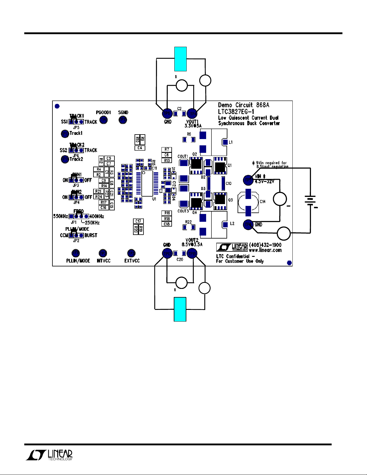
Demonstration circuit 868 is easy to set up to evaluate
the performance of the LTC3827-1. Refer to Figure 1 for
proper measurement equipment setup and follow the
procedure below:
1.
Place RUN1 and RUN2 in OFF position, the FREQ
jumper at the selected frequency and the
PLLIN/MODE jumper JP2 in desired Mode (Burst or
CCM Mode) position. Table 2 shows the default set-
JP1
FREQ
400kHz BURST ON ON SS1 SS2
JP2
PLL/MODE
JP3
RUN1
JP4
RUN2
Table 2. Default Jumper Settings
2.
Connect the desired loads between 3.3V and 8.5V
terminals and their closest PGND terminals on the
board.
ting for DC868.
94%
98%
JP5
TRACK1
JP6
TRACK2
Page 2

QUICK START GUIDE FOR DEMONSTRATION CIRCUIT 868
2
JP6 Set
Function
R28 R29
LOW QUIESCENT CURRENT DUAL SYNCHRONOUS BUCK CONVERTER
NOTE:
The maximum load at 3.3V is 5A, and the
maximum at 8.5V is 3.5A.
3.
Connect the input power supply to the VIN and GND
terminals on the right, center of the board.
NOTE:
Do not increase VIN over 32V.
4.
Switch on the desired channel(s) by moving the
RUN1 and/or RUN2 jumper to “on” position.
The following table shows the different output tracking options for Vout1 and Vout2
JP5 Set Function R25 R26 R27
5.
Measure the output voltages. They should be 3.3V
±
0.066V and 8.5V ±0.17V respectively, within each
specified maximum load current.
6.
For better efficiency at high input voltage, tie EXTVCC
to external source of 5V-9V or mount the optional resistor R1(0 ohm).
7.
If external synchronization is desired, remove JP2 and
tie PLLIN/MODE to external clock signal. Please refer
to datasheet for more details.
SS1* SS w/o tracking DNP DNP DNP
TRACK Track Track1 35.7k 11.5k DNP
SS2* SS w/o tracking DNP DNP
TRACK Track Track2 TBD* TBD*
TRACK Track Vout2 35.7k 11.5k zero
Table 3. Tracking Jumper Settings
*With default JP5 and JP6 setting, Vout1 and Vout2 will start independently. Please refer to datasheet for TBD
value calculation.
Page 3
QUICK START GUIDE FOR DEMONSTRATION CIRCUIT 868
3
LOW QUIESCENT CURRENT DUAL SYNCHRONOUS BUCK CONVERTER
Load
Load
Load
Load
++++
A
A
A
V
V
V
V
A
Power
Power
Power
supply
supply
supply
+
+
+
V
V
V
++++
++++
++++
A
A
V
V
VAV
++++
Load
Load
Load
A
A
A
Figure 1. Proper Measurement Equipment Setup
Page 4
QUICK START GUIDE FOR DEMONSTRATION CIRCUIT 868
4
LOW QUIESCENT CURRENT DUAL SYNCHRONOUS BUCK CONVERTER
Page 5

Mouser Electronics
Authorized Distributor
Click to View Pricing, Inventory, Delivery & Lifecycle Information:
Analog Devices Inc.:
DC868A
 Loading...