

Page 1
UC1526
UC2526
UC3526
DESCRIPTION
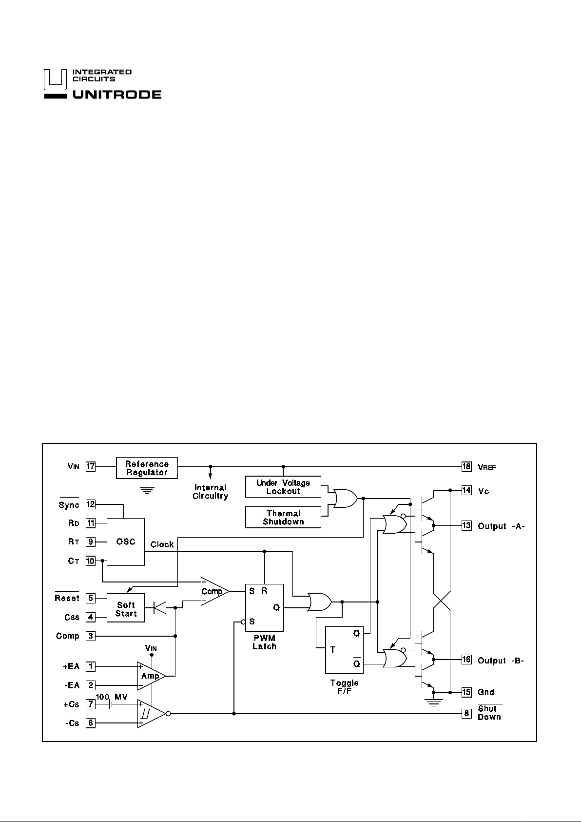
The UC1526 is a high performance monolithic pulse width modulator
circuit designed for fixed-frequency switching regulators and other
power control appl ications. Included in an 18-pin dual-in-line package are a temperature compensated voltage reference, sawtooth oscillator, error amplifier, pulse width modulator, pulse metering and
setting logic, and two low impedance power drivers. Also included
are protective features such as soft-start and under-voltage lockout,
digital current limiting, double pulse inhibit, a data latch for single
pulse metering, adjustable deadtime, and provision for symmetry correction inputs. For ease of interface, all digital control ports are TTL
and B-series CMOS compatible. Active LOW logic design allows
wired-OR connections for maximum flexibilit y. This versatile device
can be used to impl ement single-ende d or push-p ull switching regulators of either polarity, both transformerless and transformer coupled. The UC1526 is characterized for operation over the full military
temperature range of -55°C to +125°C. The UC2526 is characterized
for operation from -25°C to +85°C, and the UC3526 is characterized
for operation from 0° to +70°C.
Regulating Pulse Width Modulat or
FEATURES
• 8 To 35V Operation
• 5V Reference Trimmed To ±1%
• 1Hz To 400kHz Oscillator Range
• Dual 100mA Source/Sink Outputs
• Digital Current Limiting
• Double Pulse Suppression
• Programmable Deadtime
• Under-Voltage Lockout
• Single Pulse Metering
• Programmable Soft-Start
• Wide Current Limit Common Mode Range
• TTL/CMOS Compatible Logic Ports
• Symmetry Correction Capability
• Guaranteed 6 Unit Synchronization
BLOCK DIAGRAM
6/93
Page 2
ABSOLUTE MAXI MUM RATING S (Note 1, 2)
Input Voltage (+VIN) . . . . . . . . . . . . . . . . . . . . . . . . . . . . . . +40V
Collector Supply Voltage (+V
C) . . . . . . . . . . . . . . . . . . . . . +40V
Logic Inputs . . . . . . . . . . . . . . . . . . . . . . . . . . . . . -0.3V to +5.5V
Analog Inputs . . . . . . . . . . . . . . . . . . . . . . . . . . . . . -0. 3V to +V
IN
Source/S ink Load Current (ea ch out pu t) . . . . . . . . . . . . . 200mA
Referen ce Loa d Curr ent. . . . . . . . . . . . . . . . . . . . . . . . . . . 50mA
Logic Sink Curren t . . . . . . . . . . . . . . . . . . . . . . . . . . . . . . . 15mA
Power Dissipation at T
A = +25°C (Note 2) . . . . . . . . . . 1000mW
Power Dissipation at T
C = +25°C (Note 2). . . . . . . . . . 3000mW
Operating Junct ion Te mp era tu re . . . . . . . . . . . . . . . . . . +150°C
Storage Tem per ature Range . . . . . . . . . . . . . . -65°C to +150°C
Lead Temp era ture (solder ing, 10 sec onds ). . . . . . . . . . +300°C
Note 1: Values beyo nd which dama ge may occ ur.
Note 2: Consult packaging section of databo ok for ther m al
limitations and co nsider ations of pac kage .
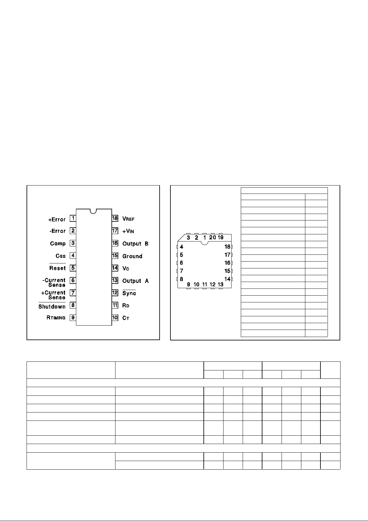
CONNECTION DIAGRAMS
UC1526
UC2526
UC3526
DIL-18, SOIC- 18 (T O P VIEW)
J or N Package, DW Package
RECOMMENDED OPERATING CONDITIONS (Note 3)
Input Voltage . . . . . . . . . . . . . . . . . . . . . . . . . . . . . . +8V to +35V
Collector Supply Voltage . . . . . . . . . . . . . . . . . . . +4.5V to +35V
Sink/Source Load Current (each output ). . . . . . . . . 0 to 100mA
Reference Load Cur re nt . . . . . . . . . . . . . . . . . . . . . . 0 to 20mA
Oscillator Frequency Range . . . . . . . . . . . . . . . . 1Hz to 400kHz
Oscillator Timing Resistor . . . . . . . . . . . . . . . . . . . 2kΩ to 150kΩ
Oscillator Timing Capacito r . . . . . . . . . . . . . . . . . . . 1nF to 20µF
Available Deadtime Range at 40kHz. . . . . . . . . . . . . 3% to 50%
Operating Am bient Temper at ur e Range
UC1526 . . . . . . . . . . . . . . . . . . . . . . . . . . . . -55°C to +125°C
UC2526 . . . . . . . . . . . . . . . . . . . . . . . . . . . . . -25°C to +85°C
UC3526 . . . . . . . . . . . . . . . . . . . . . . . . . . . . . . -0°C to +70°C
Note 3: Range over which the device is funct ional and
parameter lim its are guarant eed.
PACKAGE PIN FUNCTION
FUNCTION PIN
N/C 1
+Error 2
-Error 3
Comp. 4
CSS 5
Reset
______
6
- Current Sense 7
+ Current Sense 8
Shutdown
_________
9
RTIMING 10
CT 11
RD 12
Sync 13
Output A 14
VC 15
N/C 16
Ground 17
Output B 18
+VIN 19
VREF 20
PLCC-20, LCC-20
(TOP VIEW )
Q and L Packages
ELECTRICAL CHARACTERISTICS:
PARAMETER TEST CONDITIONS UC1526 / UC2526 UC3526 UNITS
MIN TYP MAX MIN TYP MAX
Reference Sec tio n (Note 4)
Output Volt age T
J = + 25°C 4.95 5.00 5.05 4.90 5.00 5.10 V
Line Regulation +V
IN = 8 to 35V 10 20 10 30 mV
Load Regulation I
L = 0 to 20mA 10 30 10 50 mV
Temperature Stability Over Operating T
J 15 50 15 50 mV
Total Output
Voltage Range
Over Recommended
Operating Con dition s
4.90 5.00 5.10 4.85 5.00 5.15 V
Short Circuit Current V
REF = 0V 25 50 100 25 50 100 mA
Under -Voltage Lockout
RESET
_______
Output Volt age V
REF = 3.8V 0.2 0.4 0.2 0.4 V
V
REF = 4.8V 2.4 4.8 2.4 4.8 V
Note 4: IL = 0mA.
+VIN = 15V, and over o perating ambient temperature, unless otherw ise
specified, TA = TJ.
2
Page 3
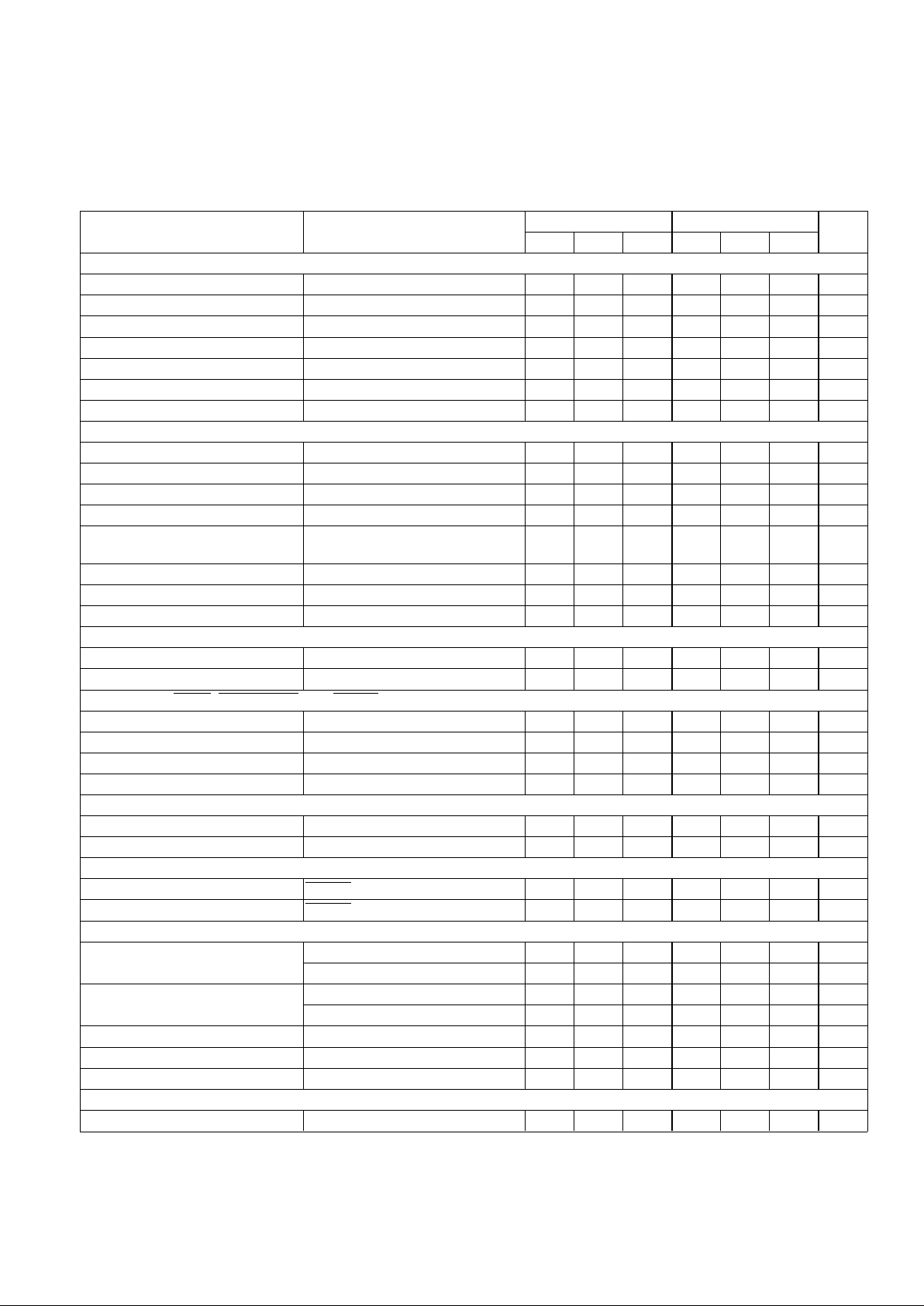
ELECTRICAL CHARACTERIST ICS :
PARAMETER TEST CONDI TIO NS UC1526 / UC2526 UC3526 UNITS
MIN TYP MAX MIN TYP MAX
Oscillator Section (Note 5)
Initial Accuracy T
J = + 25°C ±3 ±8 ±3 ±8%
Voltage Sta bi lity +V
IN = 8 to 35V 0.5 1 0.5 1 %
Temperature Stability Over Operating T
J 710 3 5%
Minimum Frequency R
T = 150kΩΩ, CT = 20µµF11Hz
Maximum Fr eque ncy R
T = 2kΩΩ, CT = 1.0nF 400 400 kHz
Sawtooth Peak Volt age +V
IN = 35V 3.0 3.5 3.0 3.5 V
Sawtooth Valley Voltage +V
IN = 8V 0.5 1.0 0.5 1.0 V
Err or Am p lifier Se cti o n (Note 6)
Input Offset Voltage R
S ≤≤ 2kΩΩ 25 210mV
Input Bias Current -350 -1000 -350 -2000 nA
Input Offset Current 35 100 35 200 nA
DC Open Loop Gain R
L ≥ 10MΩΩ 64 72 60 72 dB
HIGH Output Volt age V
PIN1-VPIN2 ≥≥ 150m V, ISOURCE =
100µµA
3.6 4.2 3.6 4.2 V
LOW Output Voltage V
PIN2-VPIN1 ≥≥ 150mV, ISINK = 100µµA 0.2 0.4 0.2 0.4 V
Common Mode Rejection Rs ≤ 12kΩ 70 94 70 94 dB
Supply Voltage Rejec tion +V
IN = 12 to 18V 66 80 66 80 dB
PWM Compar ator (Note 5)
Minimum Duty Cycle V
COMPENSATION = +0.4V 0 0 %
Maximum Duty Cycle V
COMPENSATION = +3.6V 45 49 45 49 %
Digital Ports (
SYNC, SHUTDOWN, and RESET)
HIGH Output Volt age I
SOURCE =40µµA 2.4 4.0 2.4 4.0 V
LOW Output Voltage I
SINK = 3.6mA 0.2 0.4 0.2 0.4 V
HIGH Input Curren t V
IH = +2.4V -125 -200 -125 -200 µA
LOW Input Current V
IL = +0.4V -225 -360 -225 -360 µA
Current LImit Comparator ( Not e 7)
Sense Voltage R
S ≤≤ 50ΩΩ 90 100 110 80 100 120 mV
Input Bias Current -3 -10 -3 -10 µA
Soft-Start Section
Error Clamp Voltage
RESET = +0.4V 0.1 0.4 0.1 0.4 V
Cs Charging Current
RESET =+2.4V 50 100 150 50 100 150 µA
Output Drive rs ( Each Out put ) ( Note 8)
HIGH Output Volt age I
SOURCE = 20mA 12.5 13.5 12.5 13.5 V
I
SOURCE = 100m A 12 13 12 13 V
LOW Output Voltage I
SINK = 20mA 0.2 0.3 0.2 0.3 V
I
SINK = 100mA 1.2 2.0 1.2 2.0 V
Collector Leakage V
C = 40V 50 150 50 150 µA
Rise Time CL = 1000pF 0.3 0.6 0.3 0.6 µs
Fall Time CL = 1000pF 0.1 0.2 0.1 0.2 µs
Power Consumption (Note 9)
Standby Curre nt SHUTDOW N
____________
=
+0.4V 18 30 18 30 mA
+VIN = 15V, and over operating ambient temper atur e, unless othe rwise
specified, TA = TJ.
UC1526
UC2526
UC3526
Note 4: IL = 0mA.
Note 5: F
OSC
= 40kHz (RT = 4.12k
Ω ±
1%, CT = 0.1µF ± 1%,
R
D
= 0Ω)
Note 6: V
CM
= 0 to +5.2V
Note 8: V
C
= +15V
Note 9: +V
IN
= +35V, RT = 4.12k
Ω
3
Page 4
UC1526
UC2526
UC3526
APPLICATIONS INFORMATION
Voltage Referenc e
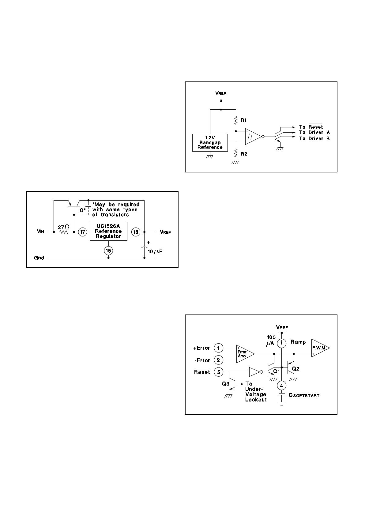
The reference regulator of the UC1526 is based on a tem-
perature compensated ze ner diode. The circuitry is fully
active at supply voltag es above +8V, and provides up to
20mA of load current to external circuitry at +5.0V. In systems where additional current is required, an external
PNP transistor can be used to boost the available current.
A rugged low frequency audio-type transistor should be
used, and lead lengths between the PWM and transistor
should be as sho rt as possible to minimize the risk of oscillations. Even so, some types of transistors may require
collector-base capacitance for stability. Up to 1 amp of
load current can b e obtained with excellent regulati on if
the device selected maintains high current gain.
Under-Voltage Lockout
The under-voltage lockout circuit protects the UC1526
and the power devices it controls from inadequate supply
voltage, If +V
IN is too low, the circuit disables the output
drivers and holds the RESET
_______
pin LOW. This prevents
spurious output pulses w hile the control circuitry is stabilizing, and holds the soft-start timing capacitor in a discharged state.
The circuit consists of a +1.2V bandgap reference and
comparator circuit which is active when the reference
voltage has risen to 3V
BE or +1.8V at 25°C. When the ref-
erence voltage rises to approximately +4.4V, the circuit
enables the output drivers an d releases the RESET
_______
pin,
allowing a normal soft-start. The comparator has 200mV
of hysteresis to minimize oscillation at the trip point.
When +V
IN to the PWM is removed and the reference
drops to +4.2V, the under-voltage circuit pulls RESET
_______
LOW again. The soft-start capacitor is immediately discharged, and the PWM is ready for another soft-start cycle.
The UC1526 can operate from a +5V supply by connecting the V
REF pin to the +VIN pin and maintaining the sup-
ply between +4.8 and +5.2V.
Soft-Start Circuit
The soft-start circuit protects the power transistors and
rectifier diodes from high current surges during power
supply turn-on. When supply voltage is first applied to the
UC1526, the unde r-voltage lockout circuit holds RESET
_______
LOW with Q
3. Q1 is turned on, which holds the soft-start
capacitor voltage at zero. The second collector of Q
1
clamps the output of the error amplifier to ground, guaranteeing zero duty cycle at the driver outputs. When the
supply voltage reache s normal operating range, RESET
_______
will go HIGH. Q
1 turns off, allowing the internal 100mA
current source to charge C
S. Q2 clamps the error ampli-
fier output to 1V
BE above the voltage on CS. As the soft-
start voltage ramps up to +5V, the duty cycle of the PWM
linearly increases to whatever value the voltage regulation loop requires for an error null.
Digital Control Ports
The three digital control ports of the UC1526 are bi-directional. Each p in can drive TTL and 5V CMOS logic directly, up to a fan-out of 10 low-power Schottky gates.
Each pin can also be directly driven by open-collector
Figure 2. U n der -Voltag e Lock out Schem ati c
Figure 1. Extending Referen ce O ut put Current
Figure 3. Soft-Start Circuit Schemati c
4
Page 5
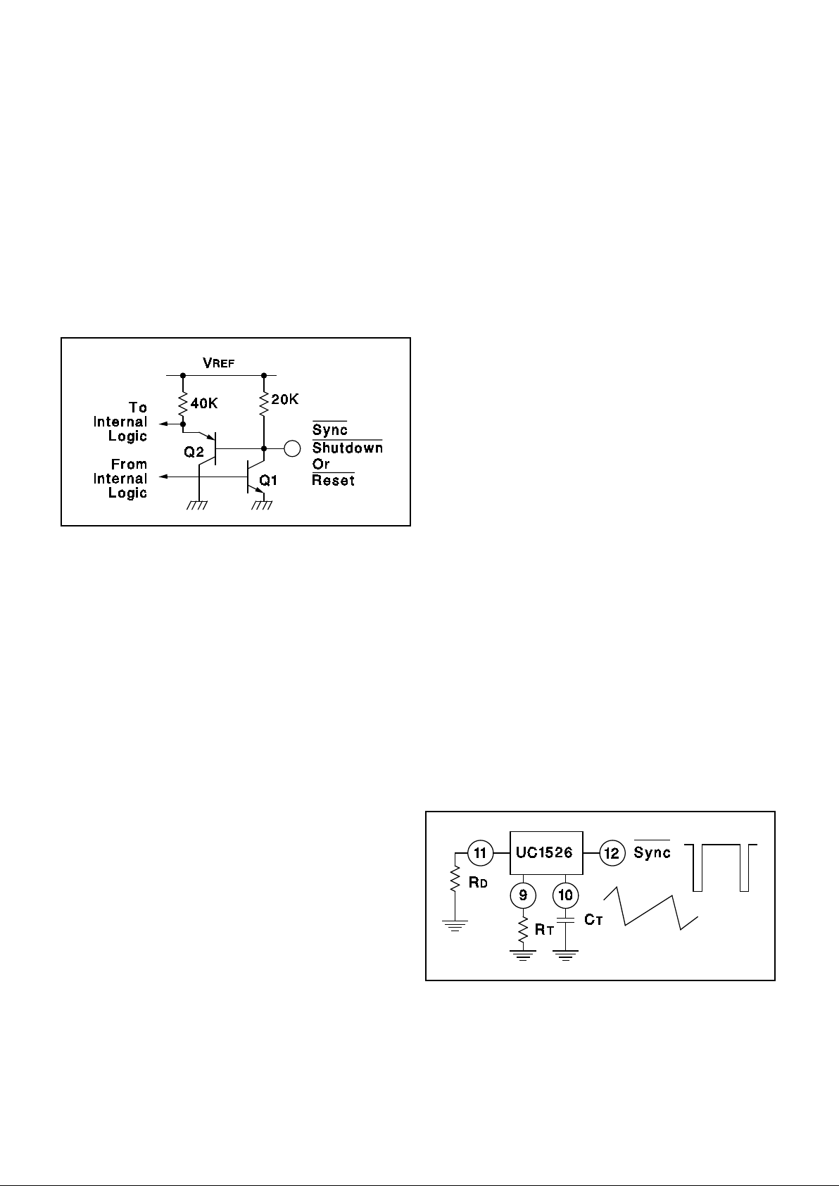
TTL, open-drain CMOS, and open-collector voltage comparators; fan-in is equivalent to 1 low-power Schottky
gate. Each port is no rmally HIGH; the pin is pulled LOW
to activate the particular function. Driving SYNC
______
LOW in-
itiates a discharge cycle in the oscillator. Pulling
SHUTDOWN
____________
LOW immediately inhibits all PWM output
pulses. Holding RESET
_______
LOW discharges the soft-start
capacitor. The logic threshold is +1.1V at +25°C. Noise
immunity can be gained at the expense of fan-out with an
external 2k pull-up resistor to +5V.
Oscillator
The oscillator is programmed for frequency and dead time
with three components: R
T, CT and RD. Two waveforms
are generated: a sawtooth wa veform at pin 10 for p ulse
width modulation, and a logic clock at pin 12. The following procedure is recommended for choosing timing values:
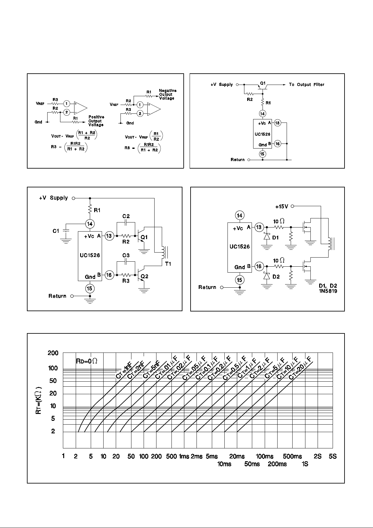
1. With R
D = 0 (pin 11 shorted to ground) select values
for R
T and CT from Figure 7 to give the desired oscillator
period. Remember that the frequency at each driver output is half the oscillator freq uency, and the frequency at
the +V
C terminal is the same as the oscillator frequency .
2. If more dead ti me is required , select a larg e value of
R
D. At 40kHz dead time increases by 400ns/ Ω .
3. Increasin g the dead time will cause the oscillator frequency to decrea se slightly. Go back and decrease the
value of R
T slightly to bring the frequency back to the
nominal design value.
The UC1526 can be synchronized to an external logic
clock by programming the oscil lator to free-run at a frequency 10% slower than the sync frequ ency. A periodic
LOW logic pulse approximately 0.5µs wide at the SYNC
______
pin will then lock the oscillator to the external frequency.
Multiple devices can be synchronized together by programming one master unit for the desired freq uency and
then sharing its sawtoo th and clock waveforms with the
slave units. All C
T terminals are connected to the CT pin
of the master, and all SYNC
______
terminals a re likewise con-
nected to the SYNC
______
pin of the master. Slave R
T termi-
nals are left open or connected to V
REF. Slave RD
terminals may be either left open or grounded.
Error Amplifier
The error ampl ifi er is a transconductance design, with an
output impedance of 2MΩ . Since all vol tage gain takes
place at the output pin, the open-loop gain/frequency
characteristics can be controlled with shunt reactance to
ground. When compensated for unity-gain stability with
100pF, the amplifier has an open-loop pole at 800Hz.
The input connections to the error amplifier are determined by the polarity of the switchi ng supply output voltage. For positi ve supplies, the common-mode voltage is
+5.0V and the feedback connections in Figure 6A are
used. With negative supplies, the common-mode voltage
is ground and the fee dback divider is connected between
the negative output and the +5.0V reference voltage, as
shown in Figure 6B.
Output Drivers
The totem-pole output drivers of the UC1526 are designed to source and sink 100mA continuously and
200mA peak. Loads can be driven either from the output
pins 13 and 16, or from the +V
C, as required.
Since the bottom transistor of the totem-pole is allowed to
saturate, there is a momentary condu ction path from the
+V
C terminal to g round during switching. To limit the re-
sulting current spikes a small resistor in series with pin 14
is always recommended. The resistor value is determined by the driver supply voltage, and should be chosen
for 200mA peak currents .
UC1526
UC2526
UC3526
Figure 5. O sc illator Connec tion s and W aveforms
Figure 4. Digital Control Port Schem at ic
APPLICATIONS INFORMATION (cont.)
5
Page 6
UC1526
UC2526
UC3526
Figure 6. Er ror Ampl ifier Connections
Figure 7. Push-Pull Configuration
Figure 8. Single-En ded Con figu rat ion
Figure 9. Driving N-channel Power Mos fets
Oscillatio n Period
TYPICAL CHARACTERIS TICS
Oscillator Period vs RT and CT
6
Page 7
UNITRODE INTEGRATED CIRCUITS
7 CONTINENTAL BLVD. • MERRIMACK, NH 03054
TEL. (603) 424-2410 • FAX (603) 424-3460
UC1526
UC2526
UC3526
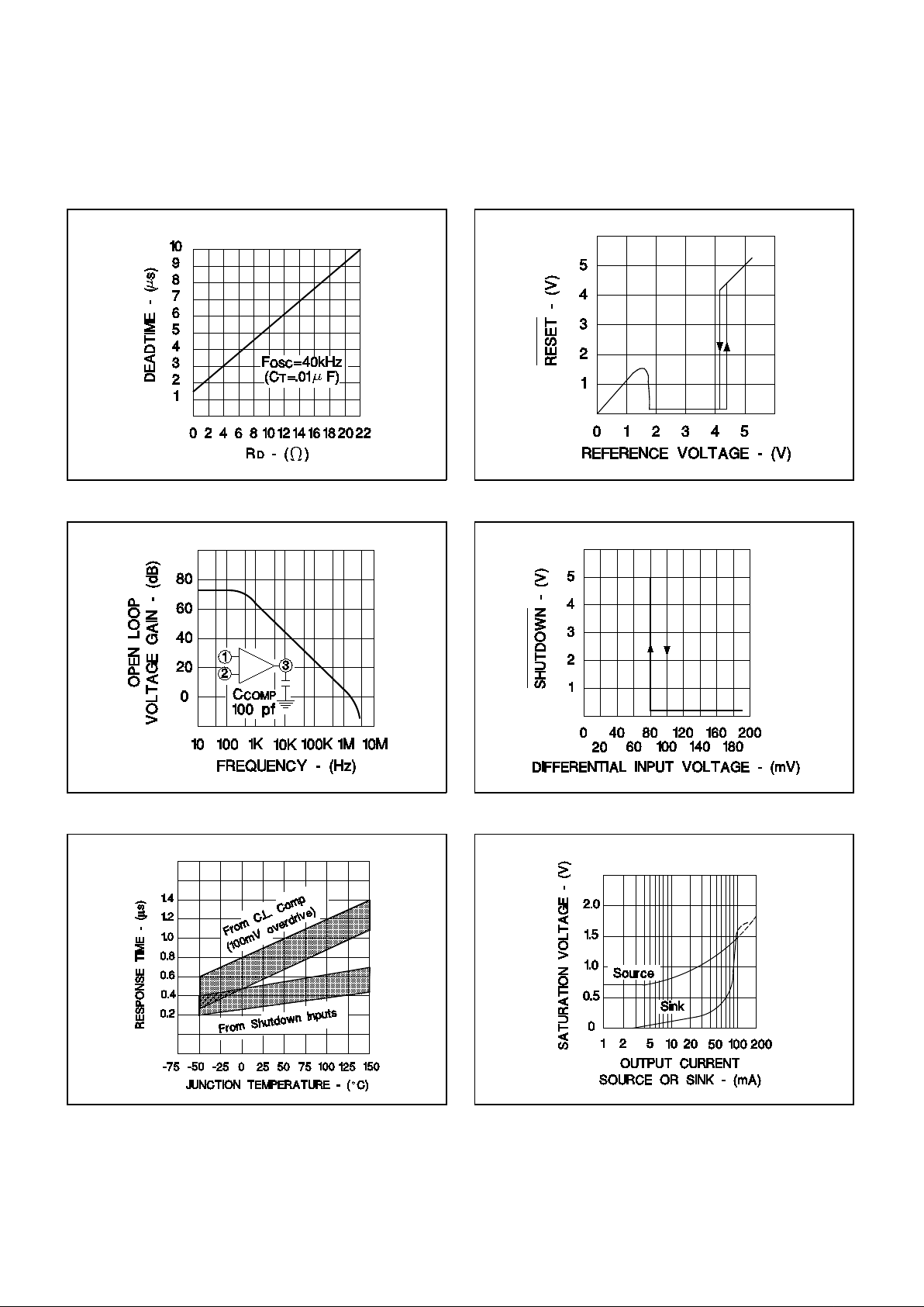
TYPICAL CHARACTERIS TICS
Shutdow n Delay Out put Driver Satu ration Voltage
Output Driver Deadtime vs R
D Value Under Voltage Lockout Characteristic
Error Amplifier Open Loop Gai n vs Freq uen c y Current Limit Tran sfer Fu nctio n
7
Page 8

IMPORTANT NOTICE
T exas Instruments and its subsidiaries (TI) reserve the right to make changes to their products or to discontinue
any product or service without notice, and advise customers to obtain the latest version of relevant information
to verify, before placing orders, that information being relied on is current and complete. All products are sold
subject to the terms and conditions of sale supplied at the time of order acknowledgement, including those
pertaining to warranty, patent infringement, and limitation of liability.
TI warrants performance of its semiconductor products to the specifications applicable at the time of sale in
accordance with TI’s standard warranty. Testing and other quality control techniques are utilized to the extent
TI deems necessary to support this warranty. Specific testing of all parameters of each device is not necessarily
performed, except those mandated by government requirements.
CERT AIN APPLICATIONS USING SEMICONDUCTOR PRODUCTS MAY INVOLVE POTENTIAL RISKS OF
DEATH, PERSONAL INJURY, OR SEVERE PROPERTY OR ENVIRONMENTAL DAMAGE (“CRITICAL
APPLICATIONS”). TI SEMICONDUCTOR PRODUCTS ARE NOT DESIGNED, AUTHORIZED, OR
WARRANTED TO BE SUITABLE FOR USE IN LIFE-SUPPORT DEVICES OR SYSTEMS OR OTHER
CRITICAL APPLICATIONS. INCLUSION OF TI PRODUCTS IN SUCH APPLICA TIONS IS UNDERSTOOD T O
BE FULLY AT THE CUSTOMER’S RISK.
In order to minimize risks associated with the customer’s applications, adequate design and operating
safeguards must be provided by the customer to minimize inherent or procedural hazards.
TI assumes no liability for applications assistance or customer product design. TI does not warrant or represent
that any license, either express or implied, is granted under any patent right, copyright, mask work right, or other
intellectual property right of TI covering or relating to any combination, machine, or process in which such
semiconductor products or services might be or are used. TI’s publication of information regarding any third
party’s products or services does not constitute TI’s approval, warranty or endorsement thereof.
Copyright 1999, Texas Instruments Incorporated
 Loading...