

Page 1

INTEGRATED CIRCUITS
80CL31/80CL51
Low-voltage single-chip
8-bit microcontrollers
Product specification 1995 January
IC20 Data Handbook
Page 2
Philips Semiconductors Product specification
80CL31/80CL51Low-voltage single-chip 8-bit microcontrollers
FEA TURES
• Full static 80C51 CPU
• 8-bit CPU, ROM, RAM, 1/0 in a single 40-lead DIL / mini-pack
• 4K x 8 ROM, expandable externally to 64K bytes
• 128 bytes RAM, expandable externally to 64K bytes
• Four 8-bit ports, 321/0 lines
• Two 16-bit timer / event counters
• External memory expandable up to 128K, external ROM up to
64K and / or RAM up to 64K
• On-chip oscillator suitable for RC, LC, quartz crystal or ceramic
resonator
• Thirteen source, thirteen vector interrupt structure with two priority
levels
• Full duplex serial port (UART)
• Enhanced architecture with:
– non-page oriented instructions
– direct addressing
– four eight byte RAM register banks
– stack depth up to 128 bytes
– multiply, divide, subtract and compare instructions
• Power-Down and IDLE instructions
• Wake-up via external interrupts at Port 1
• Single supply voltage of 1.8V to 6.0V (5.0V ±10% for P80C51)
• Frequency range of 0 to 16MHz (3.5MHz to 16MHz for P80C51)
• Very low current consumption
• Operating temperature range: -40 to +85
DESCRIPTION
The 80CL51 is manufactured in an advanced CMOS technology.
The instruction set of the 80CL51 is based on that of the 8051. The
80CL51 is a general purpose microcontroller especially suited for
battery-powered applications. The device has low power
consumption and a wide range of supply voltage. For emulation
purposes, the 85CL000 (Piggy-back version) with 256 bytes of RAM
is recommended. The 80CL51 has two software selectable modes
of reduced activity for further power reduction: Idle and Power-down.
The 80CL51 also functions as an arithmetic processor having
facilities for both binary and BCD arithmetic plus bit-handling
capabilities. The instruction set consists of over 100 instructions: 49
one-byte, 46 two-byte, and 16 three-byte.
The P80CL31 is the ROMless version of the P80CL51. P80C51 is a
5V version of the low voltage P80CL51.
The P80CL31 is the ROMless version of the P80CL51. P80C51 is a
5V version of the low voltage P80CL51.
o
C
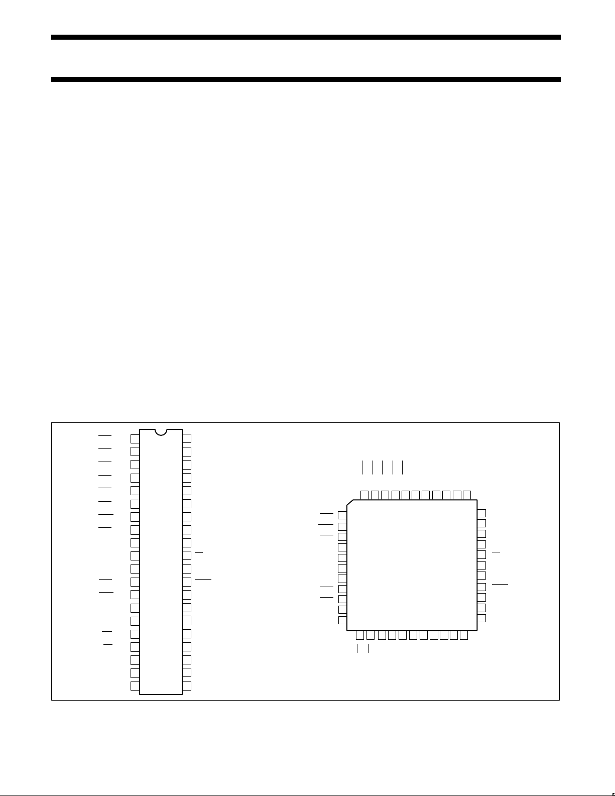
PIN CONFIGURATIONS
/P1.0
INT2
INT3/P1.1
INT4
INT5/P1.3
INT6
INT7/P1.5
INT8/
INT9
RXD/DATA/P3.0
TXD/CLOCK/P3.1
INT0
INT1/
WR
/P1.2
/P1.4
P1.6
/P1.7
RST
/P3.2
P3.3
T0/P3.4
T1/P3.5
/P3.6
RD
/P3.7
XTAL2
XTAL1
V
SS
1
2
3
4
5
6
7
8
9
10
11
12
13
PACKAGES
14
15
16
17
18
19
20
PLASTIC
DUAL
IN-LINE
SMALL
OUTLINE
AND
40
39
38
37
36
35
34
33
32
31
30
29
28
27
26
25
24
23
22
21
V
DD
P0.0/AD0
P0.1/AD1
P0.2/AD2
P0.3/AD3
P0.4/AD4
P0.5/AD5
P0.6/AD6
P0.7/AD7
EA
ALE
PSEN
P2.7/A15
P2.6/A14
P2.5/A13
P2.4/A12
P2.3/A11
P2.2/A10
P2.1/A9
P2.0/A8
P1.5/INT7
P1.6/INT8
P1.7/INT9
RST
P3.0/RXD
NC
P3.1/TXD
P3.2/INT0
P3.3/INT1
P3.4/T0
P3.5/T1
P1.4/INT6
P1.3/INT5
P1.2/INT4
P1.1/INT3
4041
424344
1
2
3
4
5
PLASTIC QUAD FLAT PACKAGE
6
7
8
9
10
11
12 13 14 15 16 17 18 19 20
XTAL2
XTAL1
P3.7/RD
P3.6/WR
DD
V
NC
P1.0/INT2
SS
V
P0.0/AD0
39 38 37 36 35 34
NC
P2.0/A8
P2.1/A9
P2.2/A10
P0.1/AD1
P0.2/AD2
2221
P2.3/A11
P0.3/AD3
33
32
31
30
29
28
27
26
25
24
23
P2.4/A12
P0.4/AD4
P0.5/AD5
P0.6/AD6
P0.7/AD7
EA
NC
ALE
PSEN
P2.7/A15
P2.6/A14
P2.5/A13
January 1995
2
Page 3
Philips Semiconductors Product specification
AND PACKAGE
NUMBER
80CL31/80CL51Low-voltage single-chip 8-bit microcontrollers
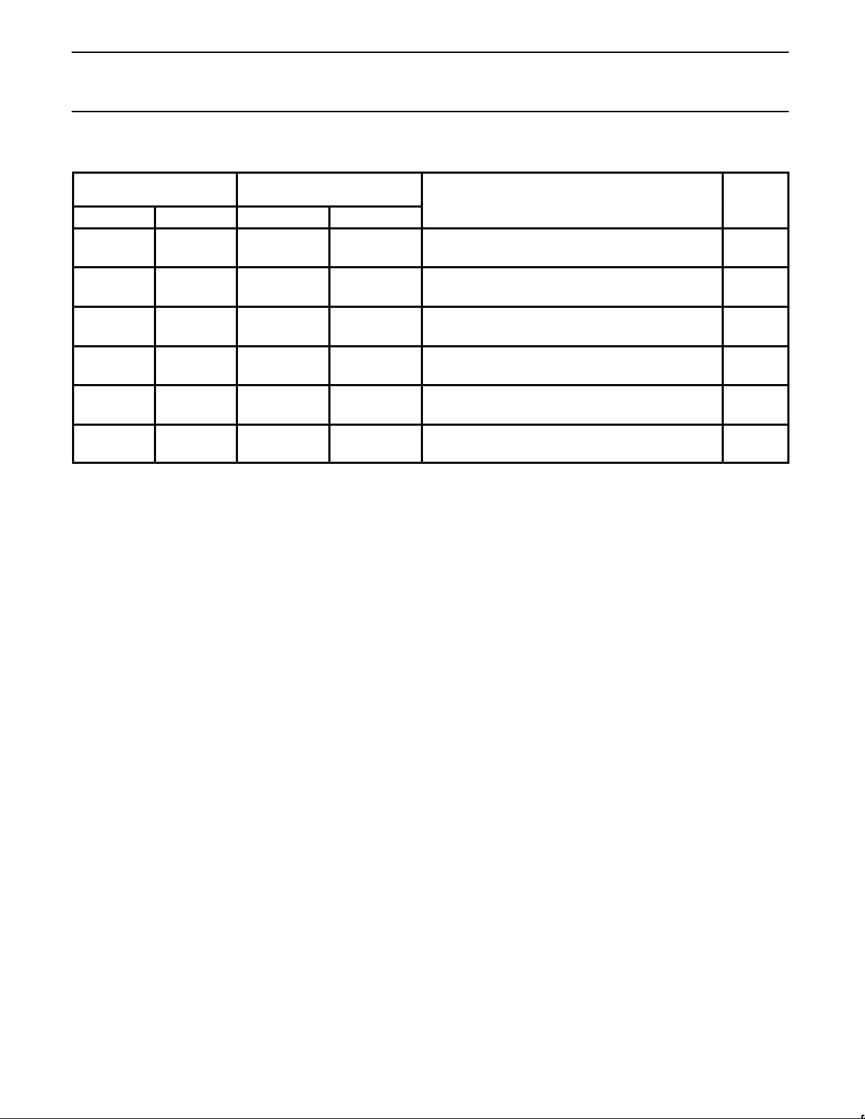
ORDERING INFORMATION
PHILIPS PART ORDER
NUMBER PART MARKING
ROMless ROM ROMless ROM
P80CL31HFP P80CL51HFP P80CL31HFP N P80CL51HFP N
P80CL31HFT P80CL51HFT P80CL31HFTD P80CL51HFT D
P80CL31HFH
NOTE:
1. Parts ordered by the Philips North America part number will be marked with the Philips part marking.
P80CL51HFH P80CL31HFH B P80CL51HFH B
P80C51HFP P80C51HFP N
P80C51HFT P80C51HFT D
P80C51HFH P80C51HFHB
PHILIPS NORTH AMERICA
PART ORDER NUMBER
1
TEMPERATURE RANGE oC
–40 to +85;
40-lead Plastic Dual In-line Package (1.8V to 6V)
–40 to +85;
40-lead Plastic Small Outline Package (1.8V to 6V)
–40 to +85;
44-lead Plastic Quad Flat Package (1.8V to 6V)
–40 to +85;
40-lead Plastic Dual In-line Package (5.0V ±10%)
–40 to +85;
40-lead Plastic Small Outline Package (5.0V ±10%)
–40 to +85;
44-lead Plastic Quad Flat Package (5.0V ±10%)
DRAWING
SOT129-1
SOT158-1
SOT307-2
SOT129-1
SOT158-1
SOT307-2
January 1995
3
Page 4
Philips Semiconductors Product specification
DESIGNATION
FUNCTION
ill
(I
alternative functions INT2 to INT9
80CL31/80CL51Low-voltage single-chip 8-bit microcontrollers
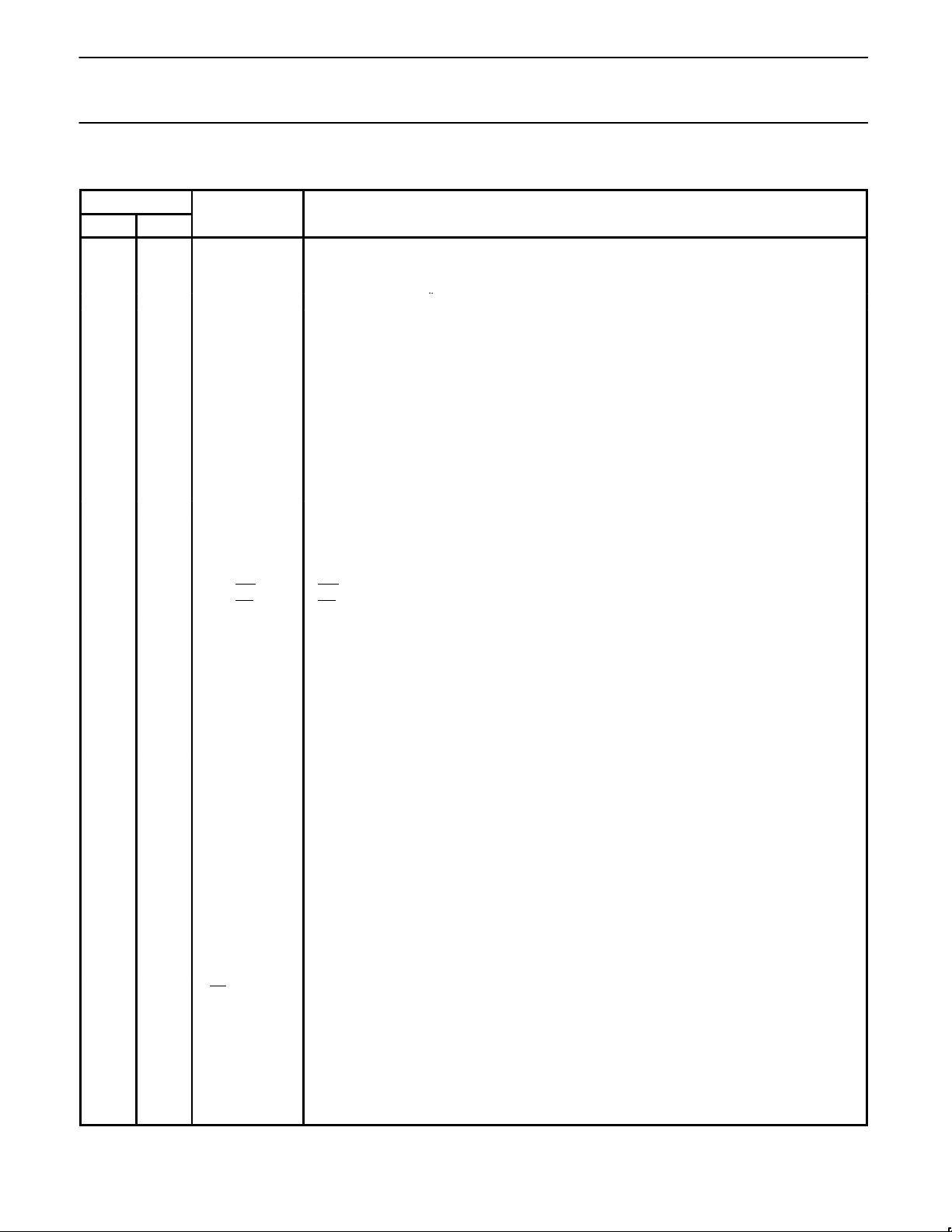
PIN DESCRIPTIONS
PIN
QFP DIP
40 1 P1.O/INT2
41 2 P1.1/lNT3
42 3 P1.2/lNT4
43 4 P1.3/INT5
44 5 P1.4/lNT6
1 6 P1.5/lNT7
2 7 P1.6/lNT8
3 8 P1.7/lNT9
4 9 RST Reset: A high level on this pin for two machine cycles while the oscillator is running resets the
5–13 10-17 Port 3: Port 3 is an 8-bit bidirectional I/O port with internal pull-ups. The Port 3 output buffers can
5 10 P3.0/RXD/data RXD/data: Serial port receiver data input (asynchronous)or data input/output (synchronous)
7 11 P3.1/TXD/clock TXD/clock: Serial port transmitter data output (asynchronous) or clock output (synchronous)
8 12 P3.2/lNT0 INT0: External interrupt 0.
9 13 P3.3/lNT1 INT1: External interrupt 1.
10 14 P3.4/T0 T0: Timer 0 external input.
11 15 P3.5/T1 T1: Timer 1 external input.
12 16 P3.6/WR WR: External data memory write strobe.
13 17 P3.7/RD RD: External data memory read strobe.
14 18 XTAL2 Crystal output: Output of the inverting amplifier of the oscillator. Left open when external clock is
15 19 XTAL1 Crystal input: Input to the inverting amplifier of the oscillator; also the input for an externally
16 20 Vss Ground: Circuit ground potential.
18-25 21-28 P2.0-P2.7 Port 2: Port 2 is an 8-bit bidirectional 1/0 port with internal pullups. Port 2 pins that have 1s written
26 29 PSEN Program store enable output: Read strobe to external program memory. When executing code
27 30 ALE Address Latch Enable: Output pulse for latching the low byte of the address during access to
29 31 EA External Access: When EA is held High the CPU executes out of internal program memory (un-
30-37 32-39 P0.0-P00.7 Port 0: Port 0 is an 8-bit open drain bidirectional I/O port. As an open drain output port it can sink 8
38 40 V
DD
Port 1: Port 1 is an 8-bit bidirectional I/O port with internal pullups. Port 1 pins that have 1s written
to them are pulled HIGH by the internal pullups, and in that state can be used as inputs. The Port 1
output buffer can sink/source 4 LS TTL loads. As inputs, Port 1 pins that are externally pulled LOW
w
source current
device.
sink/source 4 LS TTL inputs. Port 3 pins that have 1s written to them are pulled HIGH by the
internal pull ups, and in that state can be used as inputs. As inputs, Port 3 pins that are externally
pulled LOW will source current (I
used.
Crystal input: Input to the inverting amplifier of the oscillator; also the input for an externally gen-
erated clock source.
generated clock source.
to them are pulled HIGH by the internal pullups, and in that state can be used as inputs. The Port 2
output buffer can sink/source 4 LS TTL loads.
Port 2 emits the high-order address byte during accesses to external memory that use 1 6-bit addresses (MOVX @DPTR). In this application it uses the strong internal pullups when emitting 1s.
During accesses to external memory that use 8-bit addresses (MOVX @Ri), Port 2 emits the contents of the P2 Special Function Register.
out of external program memory, PSEN is activated twice each machine cycle. However, during
each access to external data memory two PSEN activations are skipped.
external memory . ALE is emitted at a constant rate of 1/6 of the oscillator frequency, and may be
used for external timing or clocking purposes.
less the program counter exceeds 0FFFH). Holding EA LOW forces the CPU to execute out of
external memory regardless of the value of the program counter.
LS TTL loads. Port 0 pins that have 1s written to them float, and in that state will function as high
impedance inputs. Port 0 is also the multiplexed low order address and data bus during access to
external memory . In this application it uses strong internal pull-ups when emitting logic 1s.
Power supply.
in the characteristics) due to the internal pullups. Port 1 also serves the
lL
.
in the characteristics) due to the internal pull ups.
lL
January 1995
4
Page 5
Philips Semiconductors Product specification
80CL31/80CL51Low-voltage single-chip 8-bit microcontrollers
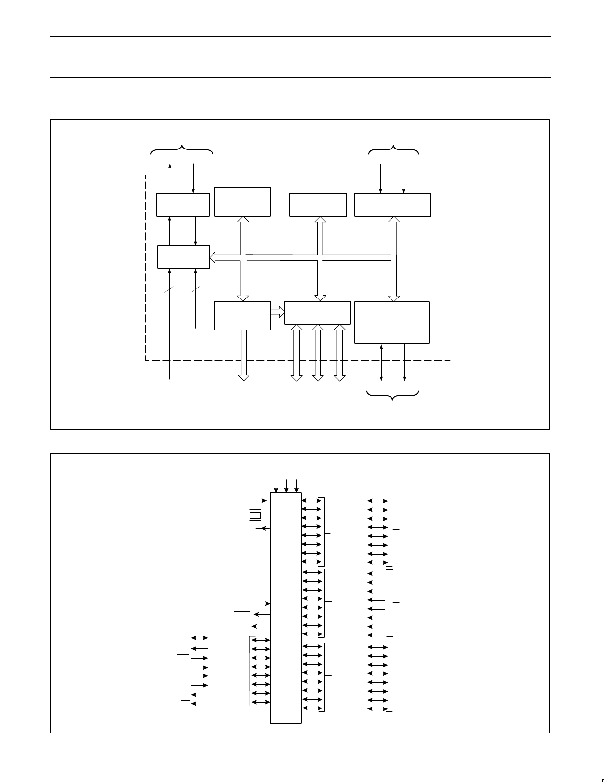
BLOCK DIAGRAM
FREQUENNCY REFERENCE
XTAL2 XTAL1
OSCILLATOR
AND TIMING
CPU
10 3
INTERNAL
INTERRUPTS
EXTERNAL ENTERRUPTS
1. Pins shared with parallels ports pins.
1
PROGRAM
MEMORY
(4K BY 8 ROM)
64K BYTE BUS
EXPANSION
CONTROL
CONTROL
DATA MEMORY
(128 BY 8 RAM)
80CL51
PROGRAMMABLE
PARALLEL PORTS
ADDRESS/DATA BUS
I/O
I/O PINS
COUNTER
T0 T1
TWO 16-BIT TIMER/
EVENT COUNTERS
PROGRAMMABLE
SERIAL PORT,
FULL DUPLEX UART,
SYNCHRONOUS
RXD TXD
1
SHIFT
(1)
FUNCTIONAL DIAGRAM
ALTERNATIVE
FUNCTIONS
RxD/data
TxD/clock
INT0
INT1
T0
T1
WR
RD
PORT 3
XTAL1
XTAL2
PSEN
ALE
EA
V
DD
V
RST
SS
PORT 0
PORT 1
PORT 2
ADDRESS AND
DATA BUS
INT2/INT9
ADDRESS BUS
January 1995
5
Page 6

Philips Semiconductors Product specification
80CL31/80CL51Low-voltage single-chip 8-bit microcontrollers
1.0 FUNCTIONAL DESCRIPTION
General
The 80CL51 is a stand-alone high-performance CMOS
microcontroller designed for use in real-time applications such as
instrumentation, industrial control, intelligent computer peripherals
and consumer products.
The device provides hardware features, architectural enhancements
and new instructions to function as a controller for applications
requiring up to 64K bytes of program memory and/or up to 64K
bytes of data storage.
The 80CL51 contains a non-volatile 4K byte × 8 read-only program
memory; a static 128 byte × 8 read/write data memory; 32 1/0 lines;
two 16-bit timer/event counters; a thirteen- source two priority-level,
nested interrupt structure and on-chip oscillator and timing circuit.
The device has two software selectable modes of reduced activity
for power reduction: IDLE and Power-down. The Idle mode freezes
the CPU while allowing the RAM, timers, serial I/O and interrupt
system to continue functioning. The Power-down mode saves the
RAM contents but freezes the oscillator causing all other chip
functions to be inoperative.
The P80C51 is a 5V version of the low voltage microcontroller
P80CL51. Hereafter the generic term P80CL51 will be used for the
functional description of both types. The special features of the
P80C51 are handled in chapter 1.9.
CPU timing
A machine cycle consists of a sequence of 6 states. Each state time
lasts for two oscillator periods, thus a machine cycle takes 12
oscillator periods or 1µs if the oscillator frequency is 12MHz.
1.1 Memory organization
The 80CL51 has a 4K Program Memory (ROM) plus 128 bytes of
Data Memory (RAM) on board. The device has separate address
spaces for Program and Data Memory (see Memory Map). Using
Ports P0 and P2, the 80CL51 can address up to 64K bytes of
external memory . The CPU generates both read and write signals
(RD and WR) for external Data Memory accesses, and the read
strobe (PSEN) for external Program Memory.
1.1.1 Program Memory
The 80CL51 contains 4K bytes of internal ROM. After reset the CPU
begins execution at location 0000H. The lower 4K bytes of Program
Memory can be implemented in either on- chip ROM or external
Memory. If the EA pin is strapped to V
, then program memory
DD
fetches from addresses 000H through 0FFFH are directed to the
internal ROM. Fetches from addresses 1000H through FFFFH are
directed to external ROM. Program counter values greater than
0FFFH are automatically addressed to external memory regardless
of the state of the EA pin.
1.1.2 Data Memory
The 80CL51 contains 128 bytes of internal RAM and 25 Special
Function Registers (SFR). The Memory Map below shows the
internal Data Memory space divided into the Lower 128, the Upper
128, and the SFR space.
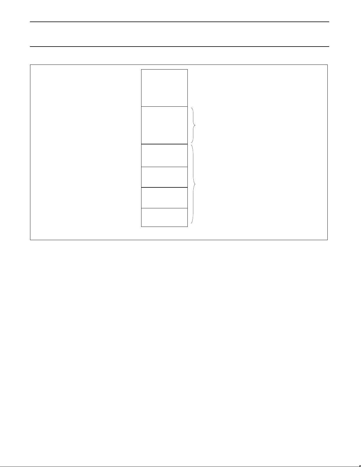
The lower 128 bytes of the internal RAM are organized as mapped
in Figure 1. The lowest 32 bytes are grouped into 4 banks of 8
registers. Program instructions refer to these registers R0 through
R7. Two bits in the Program Status Word select which register bank
is in use. The next 16 bytes above the register banks form a block of
bit-addressable memory space. The 128 bits in this area can be
directly addressed by the single-bit manipulation instructions. The
remaining registers (30H to 7FH) are directly and indirectly byte
addressable.
1.1.3 Special Function Registers
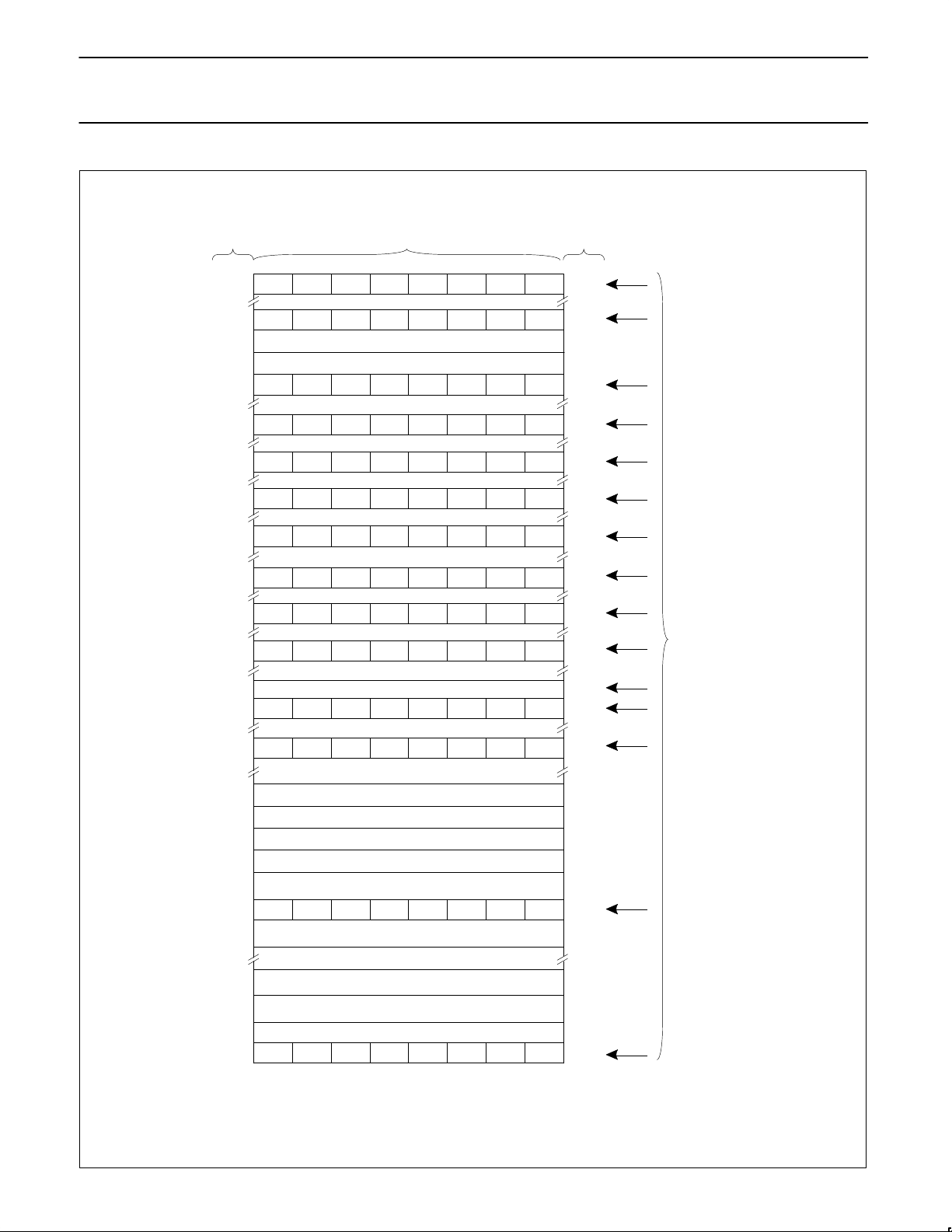
The upper 128 bytes are the address locations of the SFRs. Figure
2 shows the Special Function Register (SFR) space. SFRs include
the port latches, timers, peripheral control, serial I/O registers, etc.
These registers can only be accessed by direct addressing. There
are 128 addressable locations in the SFR address space (SFRs with
addresses divisible by eight).
1.1.4 Addressing
The 80CL51 has five methods for addressing source operands:
– Register
– Direct
– Register-lndirect
– Immediate
– Base-Register-plus Index-Register-indirect
MEMORY MAP
January 1995
4095
64K
4096
INTERNAL
= 1)
(EA
EXTERNAL
4095
INTERNAL
= 0)
(EA
225
127
0
INTERNAL
DATA RAM
INTERNAL DATA MEMORYPROGRAM MEMORY
6
OVERLAPPED
SPACE
SPECIAL
FUNCTION
REGISTERS
64K
0
EXTERNAL
DATA RAM
Page 7
Philips Semiconductors Product specification
80CL31/80CL51Low-voltage single-chip 8-bit microcontrollers
7FH
2FH
BIT-ADDRESSABLESPACE
(BIT ADDRESSES 0-7F)
20H
R7
I
I
R0
R7
I
I
R0
R7
I
I
R0
R7
I
I
R0
1FH
18H
17H
10H
0FH
08H
07H
4 BANKS OF 8 REGISTERS
(R0-R)
0
Figure 1. The Lower 128 Bytes of Internal RAM
The first three methods can be used for addressing destination
operands. Most instructions have a “destination/source” filed that
specifies data type, addressing methods and operands involved. For
operations other than MOVs, the destination operand is also a
source operand.
Access to memory addressing is as follows:
– Registers in one of the four register banks through register,
direct or indirect.
– Internal RAM (128 bytes) through direct or register-indirect.
– Special Function Register through Direct.
– External data memory through Register-lndirect
– Program memory look-up tables through Base-Register-Plus
Index-Register-Indirect.
1.2 I/O Facilities
1.2.1 Ports
The 80CL51 has 32 I/O lines treated as 32 individually addressable
bits or as four parallel 8- bit addressable ports. Port 0, 1, 2 and 3
perform the following alternate functions:
Port 0: provides the multiplexed low-order address and data bus
for expanding the device with standard memories and
peripherals.
Port 1: provides the inputs for the external interrupts INT2/lNT9.
Port 2: provides the high-order address when expanding the
device with external program or data memory.
Port 3: pins can be configured individually to provide:
(1) external interrupt request inputs
(2) counter input
(3) control signals to read and write to external memories
(4) UART input and output
To enable a Port 3 pin alternate function, the Port 3 bit latch in its
SFR must contain a logic 1.
Each port consists of a latch (Special Function Registers P0 to P3),
an output driver and an input buffer. Ports 1,2,3 have internal pull
ups. Figure 3(a) shows that the strong transistor p1 is turned on for
only 2 oscillator periods after a 0-to-1 transition in the port latch.
When on, it turns on p3 (a weak pull up) through the inverter. This
inverter and p3 form a latch which hold the 1. In Port 0 the pull up p1
is only on when emitting 1s for external memory access. Writing a 1
to a Port 0 bit latch leaves both output transistors switched off so the
pin can be used as a high-impedance input.
1.2.2 Port Options
The pins of port 1, port 2, and port 3 may be individually configured
with one of the following options (see Figure 3):
Option 1: Standard Port; quasi-bidirectional I/O with pull up. The
strong booster pull up p1 is turned on for two oscillator
periods after a 0-to-1 transition in the port latch (see
Figure 3(a)).
Option 2: Open drain; quasi-bidirectional I/O with n-channel open
drain output. Use as an output requires the connection of
an external pull up resistor (see Figure 3(c)).
Option 3: Push-Pull; output with drive capability in both polarities.
Under this option, pins can only be used as outputs. See
Figure 3(b).
January 1995
7
Page 8
Philips Semiconductors Product specification
80CL31/80CL51Low-voltage single-chip 8-bit microcontrollers
DIRECT
REGISTER
MNEMONIC
BIT ADDRESS
BYTE ADDRESS
(HEX)
IP1
IX1
IEN1
ACC
PSW
IRQ1
IP0
P3
IEN0
P2
S0BUF
S0CON
FF FE FD FC FB FA F9 F8
F7 F6 F5 F4 F3 F2 F1 F0
B
EF EE ED EC EB EA E9 E8
E7 E6 E5 E4 E3 E2 E1 E0
D7 D6 D5 D4 D3 D2 D1 D0
C7 C6 C5 C4 C3 C2 C1 C0
BD BC BB BA B9 B8
B7 B6 B5 B4 B3 B2 B1 B0
AF AE AD AC AB AA A9 A8
A7 A6 A5 A4 A3 A2 A1 A0
9F 9E 9D 9C 9B 9A 99 98
F8H
F0H
E9H
E8H
EOH
D0H
C0H
B8H
B0H
A8H
A0H
99H
98H
SFRs CONTAINING DIRECTLY
ADDRESSABLE BITS
TH1
TH0
TL1
TL0
TMOD
TCON
PCON
DPH
DPL
97 96 95 94 93 92 91 90
P1
8F 8E 8D 8C 8B 8A 89 88
SP
87 86 85 84 83 82 81 80
P0
Figure 2. Special Function Registers
90H
8DH
8CH
8BH
8AH
89H
88H
87H
83H
82H
81H
80H
January 1995
8
Page 9

Philips Semiconductors Product specification
80CL31/80CL51Low-voltage single-chip 8-bit microcontrollers
STRONG PULL UP
2 OSCILLATOR PERIODS
P2
P1
FROM
PORT
LATCH
(a)
Q
INPUT DATA
INPUT BUFFER
READ PORT PIN
n
+5V
P3
I/O PIN
STRONG PULL UP
(b)
(c)
FROM
PORT
LATCH
Q
FROM
PORT
LATCH
Q
INPUT DATA
READ PORT PIN
Figure 3. Ports
The definition of port options for port 0 is slightly different. T wo
cases have to be examined. First, accesses to external memory
(EA=0 or access above the built -in memory boundary), second, I/O
accesses.
External Memory Accesses
Option 1: True 0 and 1 are written as address to the external
memory (strong pull up is used).
Option 2: An external pull up resistor is needed for external
accesses.
Option 3: Not allowed for external memory access as the port can
only be used as output.
I/O Accesses
Option 1: When writing a 1 to the port-latch, the strong pull up p1
will be on for 2 oscillator periods. No weak pull up exists.
Without an external pull up, this option can be used as a
high-impedance input.
+5V
P1
I/O PIN
n
+5V
EXT.
PULL UP
I/O PIN
n
INPUT BUFFER
Option 2: Open drain; quasi-bidirectional I/O with n-channel open
drain output. Use as an output requires the connection of
an external pull up resistor (see Figure 3(c)).
Option 3: Push-Pull; output with drive capability in both polarities.
Under this option, pins can only be used as outputs.
Individual mask selection of the post-reset state is available on any
of the above pins. Make your selection by appending “S” or “R” to
option 1, 2, or 3 above (e.g. 1 S for a standard I/O to be set after
RESET or 2R for an open-drain I/O to be reset after RESET).
1.3 Timer/event counter
The 80CL51 contains two 16-bit Timer/Counter registers, T imer 0
and Timer 1, which can perform the following functions:
– Measure time intervals and pulse durations
– Count events
– Generate interrupts requests
January 1995
9
Page 10
Philips Semiconductors Product specification
80CL31/80CL51Low-voltage single-chip 8-bit microcontrollers
Timer 0 and Timer 1 can be independently programmed to operate
as follows:
Mode 0 - 8-bit timer or counter with divide-by-32 prescaler
1.4 Idle and Power-down operation
Idle mode operation permits the interrupt, serial port and timer
blocks to continue functioning while the clock to the CPU is halted.
The following functions remain active during Idle mode:
Mode 1 - 16-bit time-interval or event counter
Mode 2 - 8-bit time interval or event counter with automatic reload
upon overflow
Mode 3 - Timer 0 establishes TL0 and TH0 as two separate
counters.
In the “Timer” function, the register is incremented every machine
cycle. Since a machine cycle consists of 12 oscillator periods, the
count rate is 1/12 of the oscillator frequency.
In the “Counter” function, the register is incremented in response to
a 1-to-0 transition. Since it takes 2 machine cycles (24 oscillator
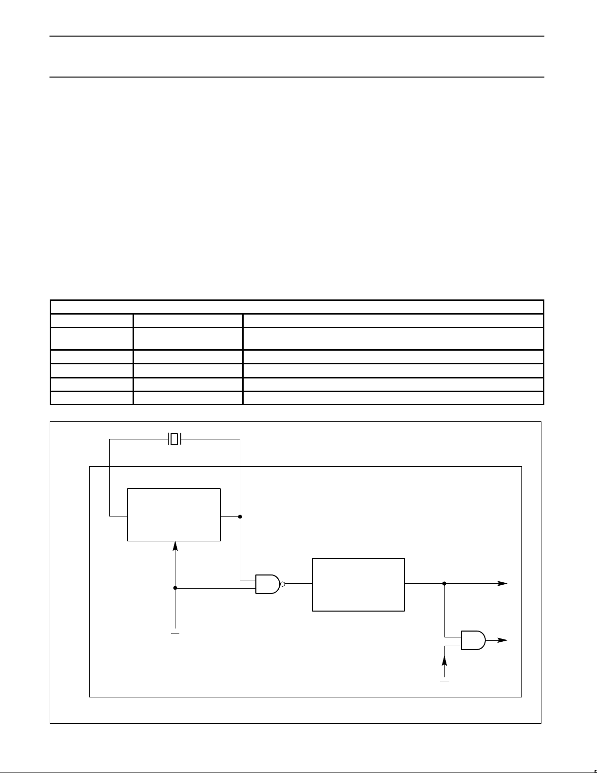
The Power-down operation freezes the oscillator. The Power-down
mode can only be activated by setting the PD bit in the PCON
register.
1.4.1 Power control register
Power-down and Idle modes are activated by software via the
Special Function Register PCON. Its hardware address is 87H.
PCON is byte addressable only.
periods) to recognize a 1-to-0 transition, the maximum count rate is
1/24 of the oscillator frequency. To ensure a given level is sampled,
it should be held for at least one full machine cycle.
PCON
BIT POSITION FUNCTION
SMOD PCON.7
PCON.4-PCON.6
Double baud-rate bit, see description of the UART, chapter 1.5.
(reserved)
GF1 PCON.3 General purpose flag bit
GFO PCON.2 General purpose flag bit
PD PCON.1 Power-down activation bit
IDL PCON.0 Idle mode activation bit
– Timer 0, Timer 1
– UART
– External interrupt
XTAL2
OSCILLATOR
PD
XTAL1
CLOCK
GENERATOR
Figure 4. Idle and Power-down Hardware
IDL
INPUTS
SERIAL PORTS
TIMER BLOCKS
CPU
January 1995
10
Page 11
Philips Semiconductors Product specification
80CL31/80CL51Low-voltage single-chip 8-bit microcontrollers
1.4.2 Power-down mode
The instruction setting PCON.1 is the last executed prior to going
into the Power-down mode. In Power-down mode the oscillator is
stopped. The contents of the on-chip RAM and SFRs are preserved.
The port pins output the values held by their respective SFRs. ALE
and PSEN are held LOW.
In the Power-down mode V
may be reduced to minimize power
DD
consumption. However, the supply voltage must not be reduced until
Power-down mode is active, and must be restored before the
hardware reset is applied and frees the oscillator. Reset must be
held active until the oscillator has restarted and stabilized.
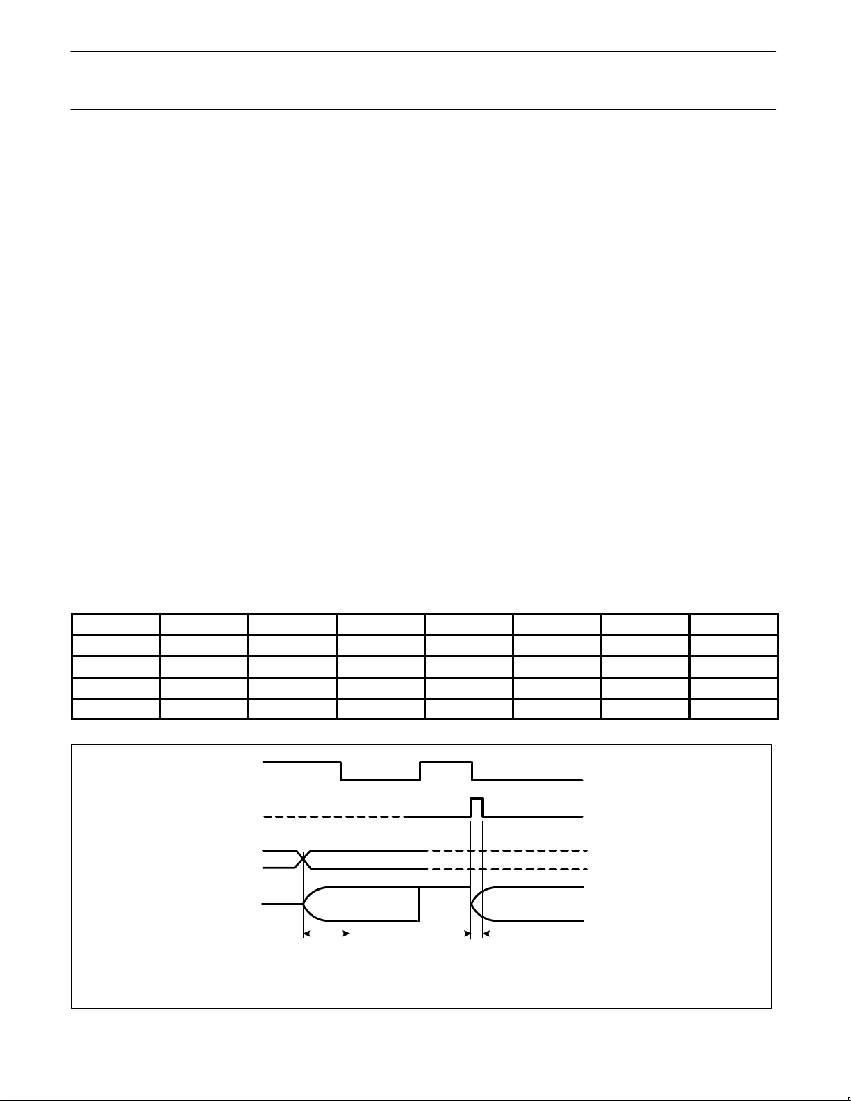
The wake-up operation after power-down in this controller has two
basic approaches:
1.4.2.1 Wake-up using INT2 to INT9
If INT2 to INT9 are enabled, the 80CL51 can be awakened from
power-down mode with the external interrupts. To ensure that the
oscillator is stable before the controller restarts, the internal clock
will remain inactive for 1536 oscillator periods. This is controlled by
an on-chip delay counter.
1.4.2.2 Wake-up using RESET
To wake-up the 80CL51 the RESET pin has to be kept HIGH for a
minimum of 24 oscillator periods. The on-chip delay counter is
inactive. The user has to ensure that the oscillator is stable before
any operation is attempted. Figure 5 illustrates the two possibilities
for wake-up.
1.4.3 Idle mode
The instruction that sets PCON.0 is the last instruction executed
before going into Idle mode. Once in the Idle mode, the internal
clock is gated away from the CPU, but not from the Interrupt, Timer
and Serial port functions. The CPU status is preserved along with
the Stack Pointer, Program Counter, Program Status Word and
Accumulator. The RAM and all other registers maintain their data
during Idle mode. The port pins retain the logical states they held at
Idle mode activation. ALE and PSEN hold at the logic HIGH level.
There are two methods used to terminate the Idle mode. Activation
of any enabled interrupt will cause PCON to be cleared by
hardware, terminating Idle mode. The interrupt is serviced, and
following the instruction RETI, the next instruction to be executed
will be the one following the instruction that put the device in the Idle
mode.
Flag bits GF0 and GF1 may be used to determine whether the
interrupt was received during normal execution or Idle mode. For
example, the instruction that writes to PCON.0 can also set or clear
one or both flag bits. When Idle mode is terminated by an interrupt,
the service routine can examine the status of the flag bits.
The second method of terminating the Idle mode is with an external
hardware reset. Since the oscillator is still running, the hardware
reset is required to be active for only two machine cycles to
complete the reset operation.
Reset redefines all SFRs, but does not affect the on-chip RAM.
The status of the external pins during Idle and Power-down mode is
shown in Table 1. If the Power-down mode is activated while
accessing external memory, port data held in the Special Function
Register P2 is restored to Port 2. If the data is a logic 1, the port pin
is held HIGH during the Power-down mode by the strong pull up
transistor p1 (see Figure 3(a)).
Table 1. Status of the External Pins During Idle and Power-down Mode
MODE MEMORY ALE PSEN PORT 0 PORT 1 PORT 2 PORT 3
Idle internal 1 1 Port Data Port Data Port Data Port Data
Idle external 1 1 Floating Port Data Address Port Data
Power-down internal 0 0 Port Data Port Data Port Data Port Data
Power-down external 0 0 Floating Port Data Port Data Port Data
POWER-DOWN
RESET-PIN
EXTERNAL INTERRUPT
OSCILLATOR
DELAY COUNTER
1536 PERIODS
Figure 5. Wake-up Operation
>24 PERIODS
January 1995
11
Page 12

Philips Semiconductors Product specification
80CL31/80CL51Low-voltage single-chip 8-bit microcontrollers
1.5 Standard serial interface SI0: UART
This serial port is full duplex, meaning it can transmit and receive
simultaneously. It is also receive-buffered, meaning it can
commence reception of a second byte before a previously received
byte has been read from the register. (However, if the first byte still
hasn’t been read by the time reception of the second byte is
complete, one of the bytes will be lost). The serial port receive and
transmit registers are both accessed at Special Function Register
S0BUF. Writing to S0BUF loads the transmit register, and reading
S0BUF loads the transmit register, and reading S0BUF accesses a
physically separate receive register.
The serial port can operate in 4 modes:
Mode 0: Serial data enters and exits through RxD. TxD outputs the
shift clock. 8 bits are transmitted/ received (LSB first). The
baud is fixed at 1/12 the oscillator frequency.
Mode 1: 10 bits are transmitted (through TxD) or received (through
RxD): a start bit (0), 8 data bits (LSB first), and a stop bit
(1). On receive, the stop bit goes into RB8 in Special
Function Register SCON. The baud rate is variable.
Mode 2: 11 bits are transmitted (through TxD) or received (through
RxD): start bit (0), 8 data bits (LSB first), a programmable
9th data bit, and a stop bit (1). On Transmit, the 9th data
bit (TB8 in SCON) can be assigned the value of 0 or 1.
Or, for example, the parity bit (P, in the PSW) could be
moved into TB8. On receive, the 9th data bit goes into
RB8 in Special Function Register SCON, while the stop
bit is ignored. The baud rate is programmable to either
1/32 or 1/64 the oscillator frequency.
Mode 3: 11 bits are transmitted (through TxD) or received (through
RxD): a start bit (0), 8 data bits (LSB first), a
programmable 9th data bit and a stop bit (1). In fact,
Mode 3 is the same as Mode 2 in all respects except
baud rate. The baud rate in Mode 3 is variable.
In all four modes, transmission is initiated by any instruction that
uses S0BUF as a destination register. Reception is initiated in Mode
0 by the condition Rl = 0 and REN = 1. Reception is initiated in the
other modes by the incoming start bit if REN = 1.
1.5.1 Multiprocessor communications
Modes 2 and 3 have a special provision for multiprocessor
communications. In these modes, 9 data bits are received. The 9th
one goes into RB8. Then comes a stop bit. The port can be
programmed such that when the stop bit is received, the serial port
interrupt will be activated only if RB8 = 1. This feature is enabled by
setting bit SM2 in SCON. A way to use this feature in multiprocessor
systems is as follows:
When the master processor wants to transmit a block of data to one
of several slaves, it first sends out an address byte which identifies
the target slave. An address byte differs from a data byte in that the
9th bit is 1 in an address byte and 0 in a data byte. With SM2 = 1, no
slave will be interrupted by a data byte. An address byte, however,
will interrupt all slaves, so that each slave can examine the received
byte and see if it is being addressed. The addressed slave will clear
its SM2 bit and prepare to receive the data bytes that will be coming.
The slaves that weren’t being addressed leave their SM2s set and
go on about their business, ignoring the coming data bytes.
SM2 has no effect in Mode 0, and in Mode 1 can be used to check
the validity of the stop bit. In a Mode 1 reception, if SM2 = 1, the
receive interrupt will not be activated unless a valid stop bit is
received.
1.5.2 Serial port control register
The serial port control and status register is the Special Function
Register S0CON, shown in Figure 6. The register contains not only
the mode selection bits, but also the 9th data bit for transmit and
receive (TB8 and RB8), and the serial port interrupt bits (T1 and
R1). See next page.
Baud Rates
The baud rate in Mode 0 is fixed: Mode 0 Baud Rate = Oscillator
Frequency /12. The baud rate in Mode 2 depends on the value of bit
SMOD in Special Function Register PCON. If SMOD = 0 (which is
the value on reset), the baud rate is 1/64 the oscillator frequency. If
SMOD = 1, the baud rate is 1/32 the oscillator frequency.
SMOD
Mode 2 Baud Rate = (2
The baud rates in Modes 1 and 3 are determined by the Timer 1
overflow rate.
Using Timer 1 to generate baud rates
When Timer 1 is used as the baud rate generator , the baud rates in
Modes 1 and 3 are determined by the Timer 1 overflow rate and the
value of SMOD as follows:
SMOD
/32)(Timer 1 Overflow Rate)
(2
The Timer 1 interrupt should be disabled in this application. The
Timer itself can be configured for either “timer” or “counter”
operation, and in any of its 3 running modes. In the most typical
applications, it is configured for “timer operation, in the auto-reload
mode (high nibble of TMOD = 0010B). In that case the baud rate is
given by the formula:
Mode 1, 3 Baud Rate =
SMOD
{(2
One can achieve very low baud rates with Timer 1 by leaving the
Timer 1 interrupt enabled, and configuring this Timer to run as a
16-bit timer (high nibble of TMOD = 0001B), and using the Timer 1
interrupt to do a 16-bit software reload. Table 2 lists various
commonly used baud rates and how they can be obtained from
Timer 1.
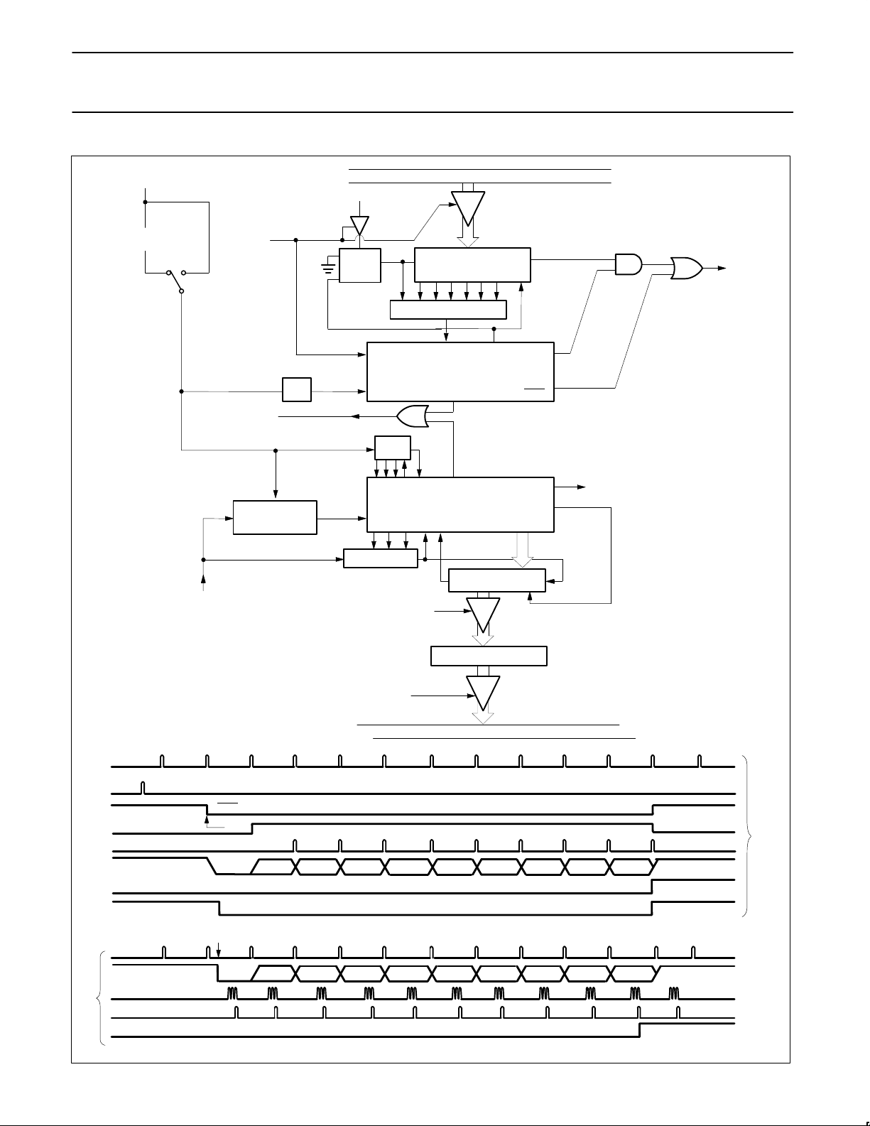
More about Mode 0
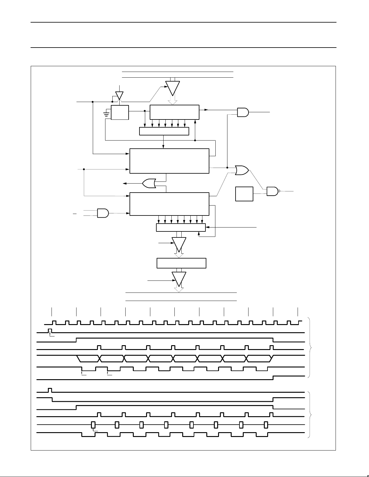
Figure 7 shows a simplified functional diagram of the serial port in
Mode 0, and associated timing. Transmission is initiated by any
instruction that uses S0BUF as a destination register. The “write to
S0BUF” signal at S6P2 also loads a 1 into the 9th position of the
transmit shift register and tells the TX Control block to commence a
transmission. The internal timing is such that the one full machine
cycle will elapse between “write to S0BUF”, and activation of SEND.
SEND enables the output of the shift register to the alternate output
function line of P3.0 and also enables SHIFT CLOCK to the
alternate output function line of P3.1. SHIFT CLOCK is low during
S3, S4, and S5 of every machine cycle, and high during S6, S1 and
S2. At S6P2 of every machine cycle in which SEND is active, the
contents of the transmit shift are shifted to the right one position.
As data bits shift out to the right, zeros come in from the left. When
the MSB of the data byte is at the output position of the shift register,
then the 1 that was initially loaded into the 9th position is just to the
left of the MSB, and all positions to the left of that contain zeros.
This condition flags the TX Control block to do one last shift and
then deactivate SEND and set T1. Both of these actions occur at
S1P1 of the 10th machine cycle after “write to S0BUF”.
Reception is initiated by the condition REN = 1 and R1 = 0. At S6P2
of the next machine cycle, the RX Control unit writes the bits
11111110 to the receive shift register, and in the next clock phase
activates RECEIVE.
/32) (Oscillator Frequency)} / {12 (256 - (TH 1 )}
/64)(Oscillator Frequency)
January 1995
12
Page 13
Philips Semiconductors Product specification
80CL31/80CL51Low-voltage single-chip 8-bit microcontrollers
MSB
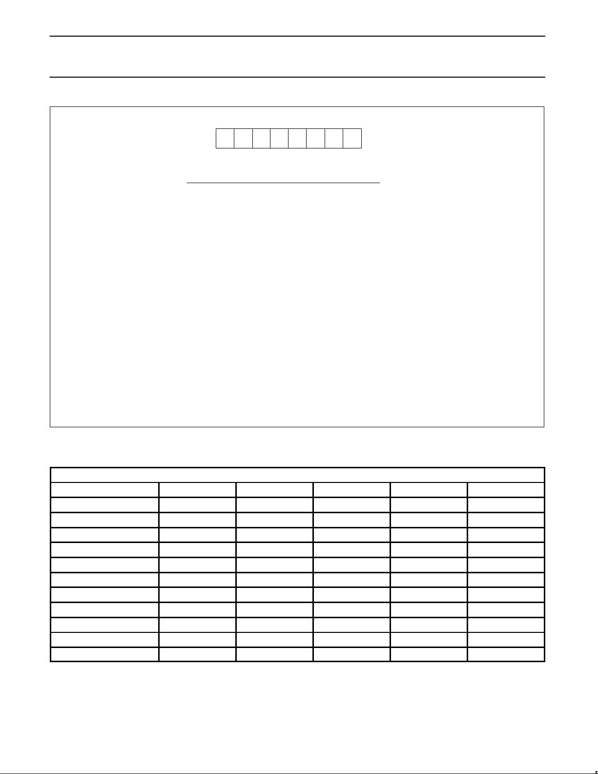
SM0 SM1 SM2 REN TB8 RB8 T1 R1
LSB
Where SM0, SM1 specify the serial port mode, as follows:
SM0 SM1 Mode Description Baud Rate
0 0 0 shift register f
OSC
/ 12
0 1 1 8-bit UART variable
1 0 2 9-bit UART f
OSC
/64
or
f
/32
OSC
1 1 3 9-bit variable UART
SM2 Enables the multiprocessor communication feature in Modes 2 and 3. In Mode 2 or 3, if SM2 is set to 1 then Rl will not
be activated if the received 9th data bit (RB8) is 0. In Mode 1, if SM2=1 then R1 will not be activated if a valid stopbit
was not received. In Mode 0, SM2 should be 0.
REN Enables serial reception. Set by software to enable reception. Clear by software to disable reception.
TB8 Is the 9th data bit that will be transmitted in Modes 2 and 3. Set or clear by software as desired.
RB8 In Modes 2 and 3, is the 9th data bit that was received. In Mode 1, it SM2=0, RB8 is the stop bit that was received. In
Mode 0, RB8 is not used.
TI Is transmit interrupt flag. Set by hardware at the end of the 8th time in Mode 0, or at the beginning of the stop bit in the
other modes, in any serial transmission. Must be cleared by software.
RI Receive interrupt flag. Set by hardware at the end of the 8th bit time in Mode 0, or halfway through the stop bit time in
the other modes, in any serial reception except (see SM2). Must be cleared by software.
Figure 6. Serial Port control (SCON) Register
Table 2. Timer 1 Generated Commonly Used Baud Rates
TIMER 1
BAUD RATE f
OSC
Mode 0 Max: 1.33 Mb/s 16 MHz x x x x
Mode 2 Max: 500 Kb/s 16 MHz 1 x x x
Modes 1,3: 83.3 Kb/s 16 MHz 1 0 2 FFH
19.2 Kb/s 11.059 MHz 1 0 2 FDH
9.6 Kb/s 11.059 MHz 0 0 2 FDH
4.8 Kb/s 11.059 MHz 0 0 2 FAH
2.4 Kb/s 11.059 MHz 0 0 2 F4H
1.2 Kb/s 11.059 MHz 0 0 2 E8H
137.5 Kb/s 11.986 MHz 0 0 2 1DH
110 6 MHz 0 0 2 72H
110 12 MHz 0 0 1 FEEBH
SMOD C/T MODE RELOAD VALUE
January 1995
13
Page 14

Philips Semiconductors Product specification
80CL31/80CL51Low-voltage single-chip 8-bit microcontrollers
RECEIVE enables SHIFT CLOCK to the alternate output function
line of P3.1. SHIFT Clock makes transitions at S3P1 and S6P1 of
every machine cycle. at S6P2 of every machine cycle in which
RECEIVE is active, the contents of the receive shift register are
shifted to the left one position. The value that comes in from the right
is the value that was sampled at the P3.0 pin at S5P2 of the same
machine cycle.
As data bits come in from the right, 1s shift out to the left. When the
0 that was initially loaded into the right-most position arrives at the
left-most position in the shift register, it flags the RX Control block to
do one last shift and load S0BUF. At S1P1 of the 10th machine cycle
after the write to SCON that cleared Rl, RECEIVE is cleared as Rl is
set.
More about Mode 1
Ten bits are transmitted (through TxD), or received (through RxD): a
start bit (0), 8 data bits (LSB first), and a stop bit (1 ). On receive,
the stop bit goes into RB8 in SCON. In the 8051 the baud rate is
determined by the Timer 1 overflow rate.
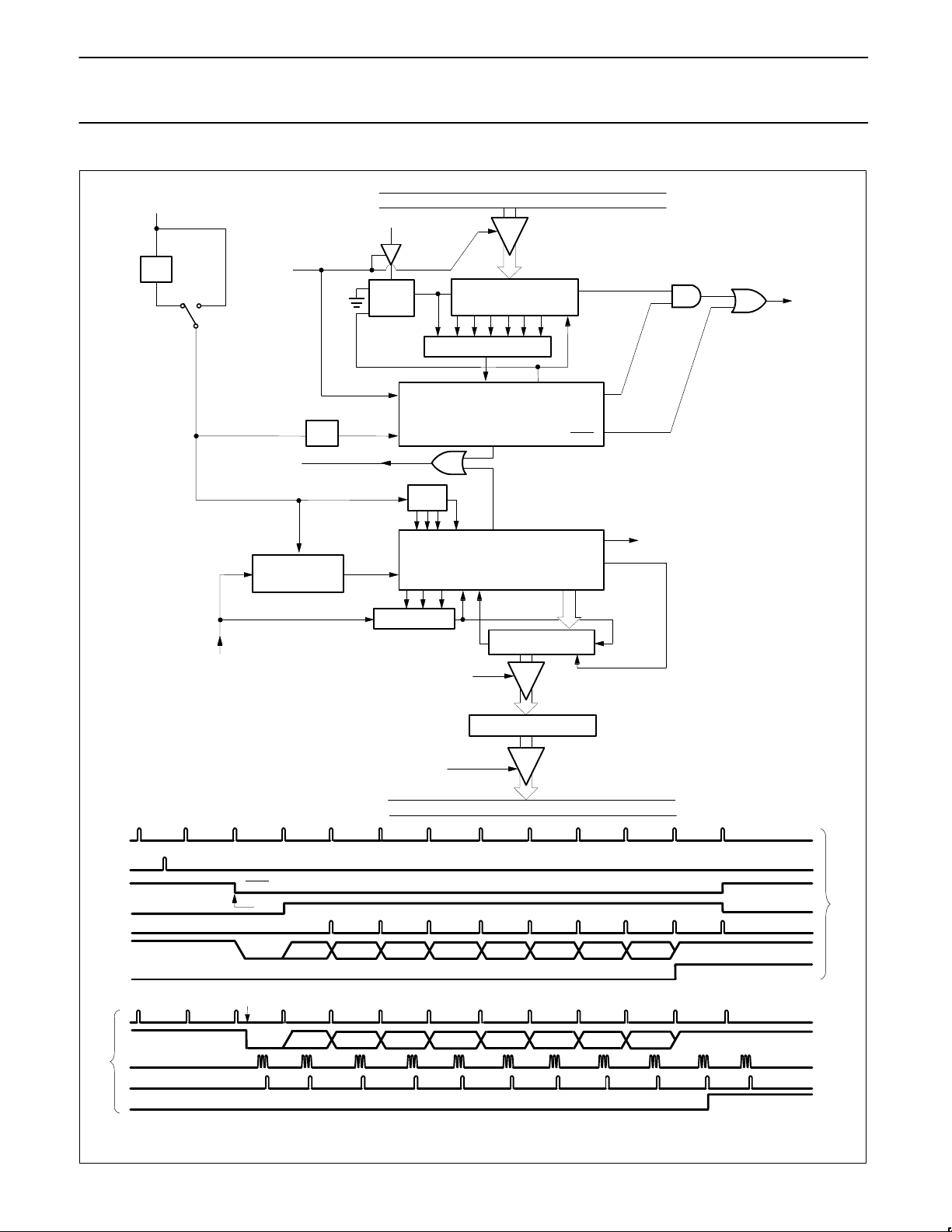
Figure 8 shows a simplified functional diagram of the serial port in
Mode 1, and associated timings for transmit/receive.
Transmission is initiated by any instruction that uses S0BUF as a
destination register . The “write to S0BUF” signal also loads a 1 into
the 9th bit position of the transmit shift register and flags the TX
Control unit that a transmission is requested. Transmission actually
commences at S1P1 of the machine cycle following the next rollover
in the divide-by-16 counter. (Thus, the bit times are synchronized to
the divide-by-16 counter, not to the “write to S0BUF” signal).
The transmission begins with activation of SEND which sends the
start bit to pin TxD. One bit time later, DATA is activated, enabling
the transmission of the output bit of the transmit shift register to TxD.
The first shift pulse occurs one bit time after that.
As data bits shift out to the right, zeros are clocked in from the left.
When the MSB of the data byte is at the output position of the shift
register, then the 1 that was initially loaded into the 9th position is
just to the left of the MSB, and all positions to the left of that contain
zeros. This condition flags the TX Control unit to do one last shift
and then deactivate SEND and set Tl. This occurs at the 10th
divide-by-16 rollover after “write to S0BUF”. Reception is initiated by
a detected 1 -to-0 transition at RxD. For this purpose RxD is
sampled at a rate of 16 times whatever baud rate has been
established. When a transition is detected, the divide-by-16 counter
is immediately reset, and 1FFH is written into the input shift register.
Resetting the divide-by-16 counter aligns its rollovers with the
boundaries of the incoming bit times. The 16 states of the counter
divide each bit time into 16th. At the 7th, 8th, and 9th counter states
of each bit time, the bit detector samples the value of RxD. The
value accepted is the value that was seen in at least 2 of the 3
samples. This is done for noise rejection. If the value accepted
during the first bit time is not 0, the receive circuits are reset and the
unit goes back to looking for another 1-to-0 transition. This is to
provide rejection of false start bits. If the start bit proves valid, it is
shifted into the input shift register, and reception of the rest of the
frame will proceed.
As data bits come in from the right, 1s shift out to the left. When the
start bit arrives at the left-most position in the shift register, (which in
mode 1 is a 9-bit register), it flags the RX Control block to do one
last shift, loads S0BUF and RB8, and set Rl. The signal to load
S0BUF and RB8, and to set Rl, will generated if, and only if, the
following conditions are met at the time the final shift pulse is
generated.
1. R1 = 0, and
2. Either SM2 = 0, or the received stop bit = 1
If either of these two conditions is not met, the received frame is
irretrievably lost. If both conditions are met, the stop bit goes into
RB8, the 8 data bits go into S0BUF, and Rl is activated. At this time,
whether the above conditions are met or not, the unit goes back to
looking for a 1-to-0 transition in RxD.
More about modes 2 and 3
Eleven bits are transmitted (through TxD), or received (through
RxD): a start bit (0), 8 data bits (LSB first), a programmable 9th data
bit, and a stop bit (1). On transmit, the 9th data bit (TB8) can be
assigned the value of 0 or 1. On receive, the 9th data bit goes into
RB8 in SCON. The baud rate is programmable to either 1/32 or 1/64
the oscillator frequency in Mode 2. Mode 3 may have a variable
baud rate generated from Timer 1.
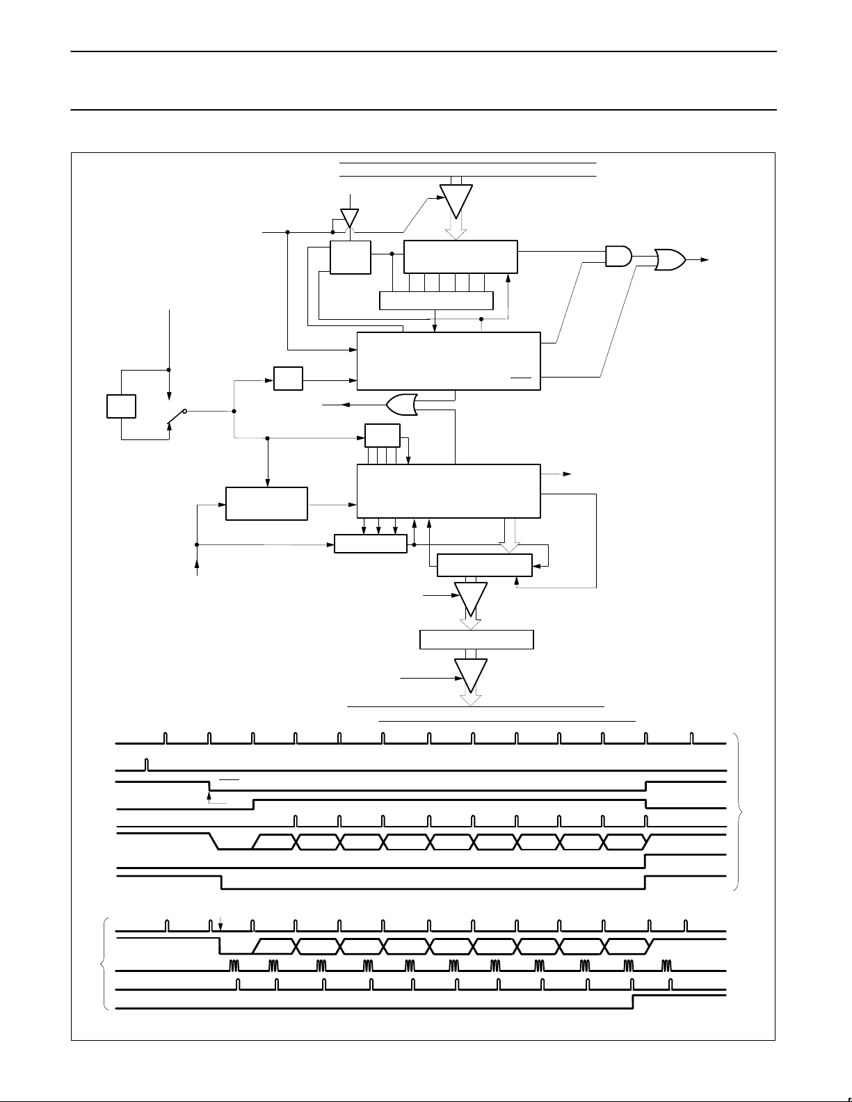
Figures 9 and 10 show a functional diagram of the serial port in
Modes 2 and 3. The receive portion is exactly the same as in Mode
1. The transmit portion differs from Mode 1 only in the 9th bit of the
transmit shift register.
Transmission is initiated by any instruction that uses S0BUF as a
destination register . The “write to S0BUF” signal also loads TB8 into
the 9th bit position of the transmit shift register and flags the TX
Control unit that a transmission is requested. Transmission
commences at S1P1 of the machine cycle following the next rollover
in the divide-by-16 counter (thus, the bit times are synchronized to
the divide-by-16 counter, not to the “write to S0BUF” signal). The
transmission begins with activation of SEND, which puts the start bit
at TxD. One bit time later, DATA is activated, which enables the
output bit of the transmit shift register to TxD. One bit time later,
DATA is activated, which enables the output bit of the transmit shift
register to TxD. The first shift pulse occurs one bit time after that.
The first shift clocks a 1 (the stop bit) into the 9th bit position of the
shift register. Thereafter, only zeros are clocked in. Thus, as data
bits shift out to the right, zeros are clocked in from the left. Then TB8
is at the output position of the shift register, then the stop bit is just to
the left of TB8, and all positions to the left of that contains zeros.
This condition flags the TX Control unit to do one last shift and then
deactivate SEND and set Tl. This occurs at the 11th divide-by-16
rollover after “write to S0BUF”.
Reception is initiated by a detected 1-to-0 transition at RxD. For this
purpose RxD is sampled at a rate of 16 times whatever baud rate
has been established. When a transition is detected, the
divide-by-16 counter is immediately reset, and 1FFFH is written to
the input shift register.
At the 7th, 8th and 9th counter states of each bit time, the bit
detector samples the value of RxD. The value accepted is the value
that was seen in at least 2 of the 3 samples. If the value accepted
during the first bit time is not 0, the receive circuits are reset and the
unit goes back to looking for another 1-to-0 transition. If the start bit
proves valid, it is shifted into the input shift register, and reception of
the rest of the frame will proceed. As data bits come in from the
right, 1s shift out to the left. When the start bit arrives at the left-most
position in the shift register (which in Modes 2 and 3 is a 9-bit
register), it flags the RX Control block to do one last shift, load
S0BUF and RB8, and set Rl.
January 1995
14
Page 15
Philips Semiconductors Product specification
80CL31/80CL51Low-voltage single-chip 8-bit microcontrollers
80CL51 Internal Bus
Write
to
SBUF
S6
REN
RI
D Q
Serial
Port
Interrupt
S
CL
Zero Detector
TX Control
TX Clock Send
Start
T1
R1
RX Control
1 1 1 1 1 1 1 0
Input Shift Register
Load
SBUF
SBUF
ShiftStart
Shift
ReceiveRX Clock
Shift
Shift
Clock
P3.0 Alt
Input
Function
RxD
RxD
P3.0 Alt
Output
Function
TxD
P3.1 Alt
Output
Function
SBUF
Read
SBUF
80CL51 Internal Bus
S4 . . S1 S6. . . . S1 S6. . . . S1 S6. . . . S1 S6. . . . S1 S6. . . . S1 S6. . . . S1 S6. . . . S1 S6. . . . S1 S6. . . . S1 S6. . . . S1
ALE
Write to SBUF
Send
Shift
RxD (Data Out) D0 D1 D2 D3 D4 D5 D6 D7
TxD (Shift Clock)
TI
RI
Receive
Shift
RxD (Data In)
TxD (Shift Clock)
S6P2
S3P1 S6P1
Write to SCON (Clear RI)
D0 D1 D2 D3 D4 D5 D6
S5P2
D7
T
r
a
n
s
m
i
t
R
e
c
e
i
v
e
January 1995
Figure 7. Serial Port Mode 0
15
Page 16
Philips Semiconductors Product specification
80CL31/80CL51Low-voltage single-chip 8-bit microcontrollers
Timer 1
Overflow
÷ 2
SMOD = 1
RxD
Write
to
SBUF
Serial
Port
Interrupt
1-to-0
Transition
Detector
÷ 16
Sample
80CL51 Internal Bus
TB8
S
D Q
CL
TX Clock Send
÷ 16
RX Clock RI
Start
Bit Detector
Load
SBUF
SBUF
Zero Detector
TX Control
T1
RX Control
Input Shift Register
Shift
(9 Bits)
DataStart
Load
SBUF
Shift
TxD
Shift
R
e
c
e
i
v
e
TX
Clock
Write to SBUF
Data
Shift
TxD
TI
RX
Clock
RxD
Bit Detector
Sample Time
Shift
RI
Send
S1P1
Start Bit
÷ 16 Reset
Start
Bit
S0 BUFFER
Read
SBUF
80CL51 Internal Bus
Figure 8. Serial Port Mode 1
T
r
a
n
s
m
i
t
Stop BitD0 D1 D2 D3 D4 D5 D6 D7
Stop BitD0 D1 D2 D3 D4 D5 D6 D7
January 1995
16
Page 17
Philips Semiconductors Product specification
80CL31/80CL51Low-voltage single-chip 8-bit microcontrollers
80CL51 Internal Bus
TB8
Write
to
Phase 2 Clock
(1/2 f
OSC
)
SBUF
S
D Q
CL
SBUF
Zero Detector
TxD
Mode 2
÷ 2
TX
Clock
SMOD = 1
SMOD = 0
(SMOD is
PCON.7)
RxD
Sample
1-to-0
Transition
Detector
÷ 16
Serial
Port
Interrupt
Stop Bit
Gen.
Start
TX Clock Send
÷ 16
Start
Bit Detector
Read
SBUF
TX Control
RX Clock
RX Control
Load
SBUF
Shift
T1
R1
Input Shift Register
(9 Bits)
S0 BUFFER
80CL51 Internal Bus
Load
SBUF
1FFH
Data
Shift
Shift
Write to SBUF
Data
Shift
TxD
TI
Stop Bit Gen.
RX
Clock
R
RxD
e
c
Bit Detector
e
Sample Times
i
Shift
v
e
RI
January 1995
Send
S1P1
Start Bit
÷ 16 Reset
Start
Bit
Figure 9. Serial Port Mode 2
17
TB8
RB8
T
r
a
n
s
m
i
Stop BitD0 D1 D2 D3 D4 D5 D6 D7
Stop BitD0 D1 D2 D3 D4 D5 D6 D7
t
Page 18
Philips Semiconductors Product specification
80CL31/80CL51Low-voltage single-chip 8-bit microcontrollers
SMOD = 0
Timer 1
Overflow
÷ 2
SMOD = 1
RxD
Write
to
SBUF
Serial
Port
Interrupt
1-to-0
Transition
Detector
÷ 16
Sample
80CL51 Internal Bus
TB8
S
D Q
CL
TX Clock Send
÷ 16
RX Clock
Start
Bit Detector
Load
SBUF
S0 BUFFER
Zero Detector
TX Control
T1
R1
RX Control
Input Shift Register
Shift
(9 Bits)
DataStart
Load
SBUF
Shift
TxD
Shift
R
e
c
e
i
v
e
TX
Clock
Write to SBUF
Data
Shift
TxD
TI
Stop Bit Gen.
RX
Clock
RxD
Bit Detector
Sample Times
Shift
RI
Send
S1P1
Start Bit
÷ 16 Reset
Start
Bit
S0 BUFFER
Read
SBUF
80CL51 Internal Bus
Figure 10. Serial Port Mode 3
TB8
RB8
T
r
a
n
s
m
i
Stop BitD0 D1 D2 D3 D4 D5 D6 D7
Stop BitD0 D1 D2 D3 D4 D5 D6 D7
t
January 1995
18
Page 19
Philips Semiconductors Product specification
80CL31/80CL51Low-voltage single-chip 8-bit microcontrollers
The signal to load S0BUF and RB8, and to set Rl, will be generated
if, and only if, the following conditions are met at the time the final
shift pulse is generated.
1. Rl = 0, and
2. Either SM2 = 0 or the received 9th data bit = 1
If either of these conditions is not met, the received frame is
irretrievably lost, and Rl is not set. If both conditions are met, the
received 9th data bit goes into RB8, and the first 8 data bits 90 into
S0BUF. One bit time later, whether the above conditions were met or
not, the unit goes back to looking for a 1-to-0 transition at the RxD
input.
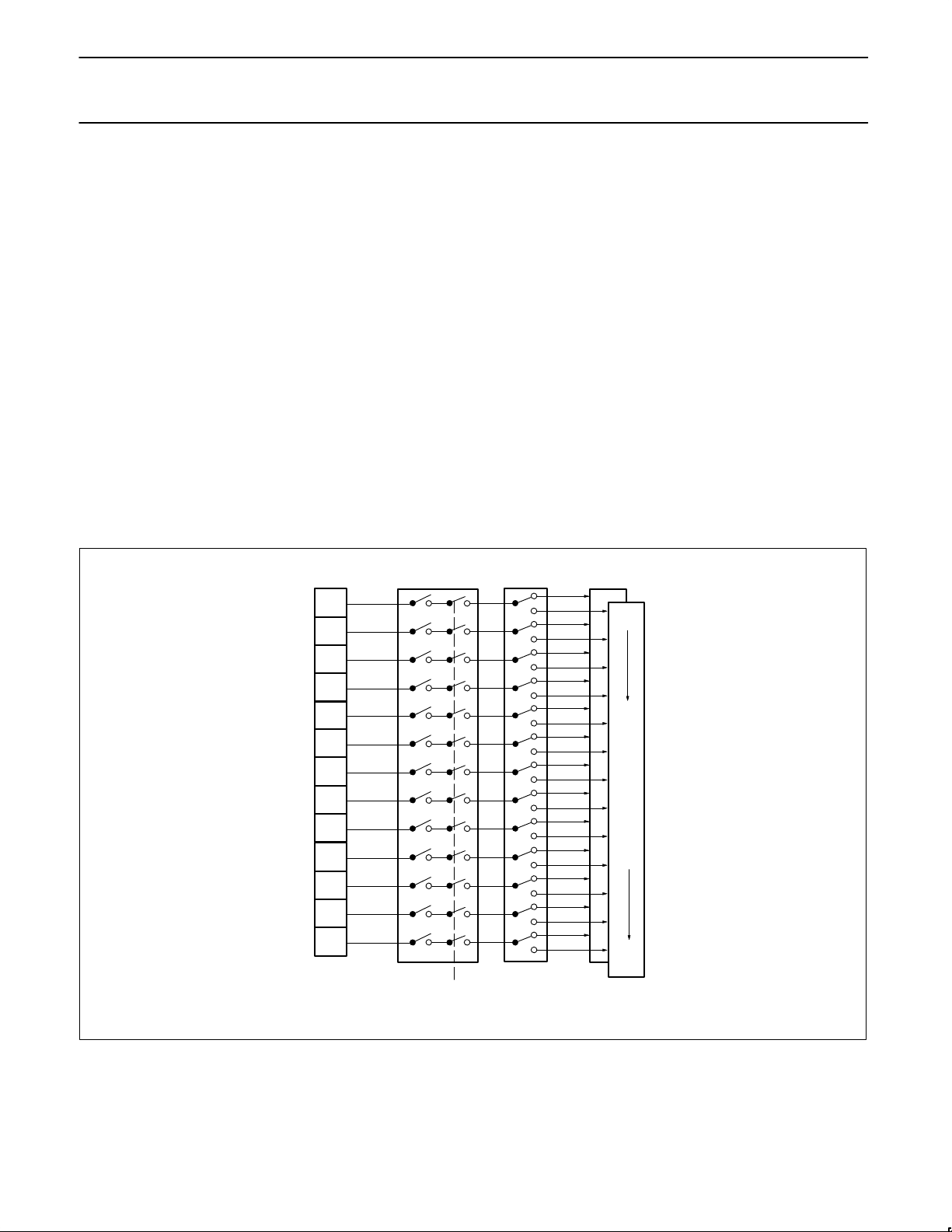
1.6 Interrupt System
External events and the real-time-driven on-chip peripherals require
service by the CPU asynchronous to do execution of any particular
section of code. To tie the asynchronous activities of these functions
to normal program execution, a multiple-source, two-priority-level,
nested interrupt system is provided. The 80CL51 acknowledges
interrupt requests from thirteen sources as follows:
– INT0 and INT1
– Timer 0 and Timer 1
INTERRUPT
SOURCES
X0
S0
IEN0/1
– UART serial I/O
– INT2 to INT9 (Port 1)
Each interrupt vectors to a separate location in program memory for
its service routine. Each source can be individually enabled or
disabled by corresponding bits in the Interrupt Enable Registers (IE,
IEO). The priority level is selected via the Interrupt Priority register
(IP0, IP1). All enabled sources can be globally disabled or enabled.
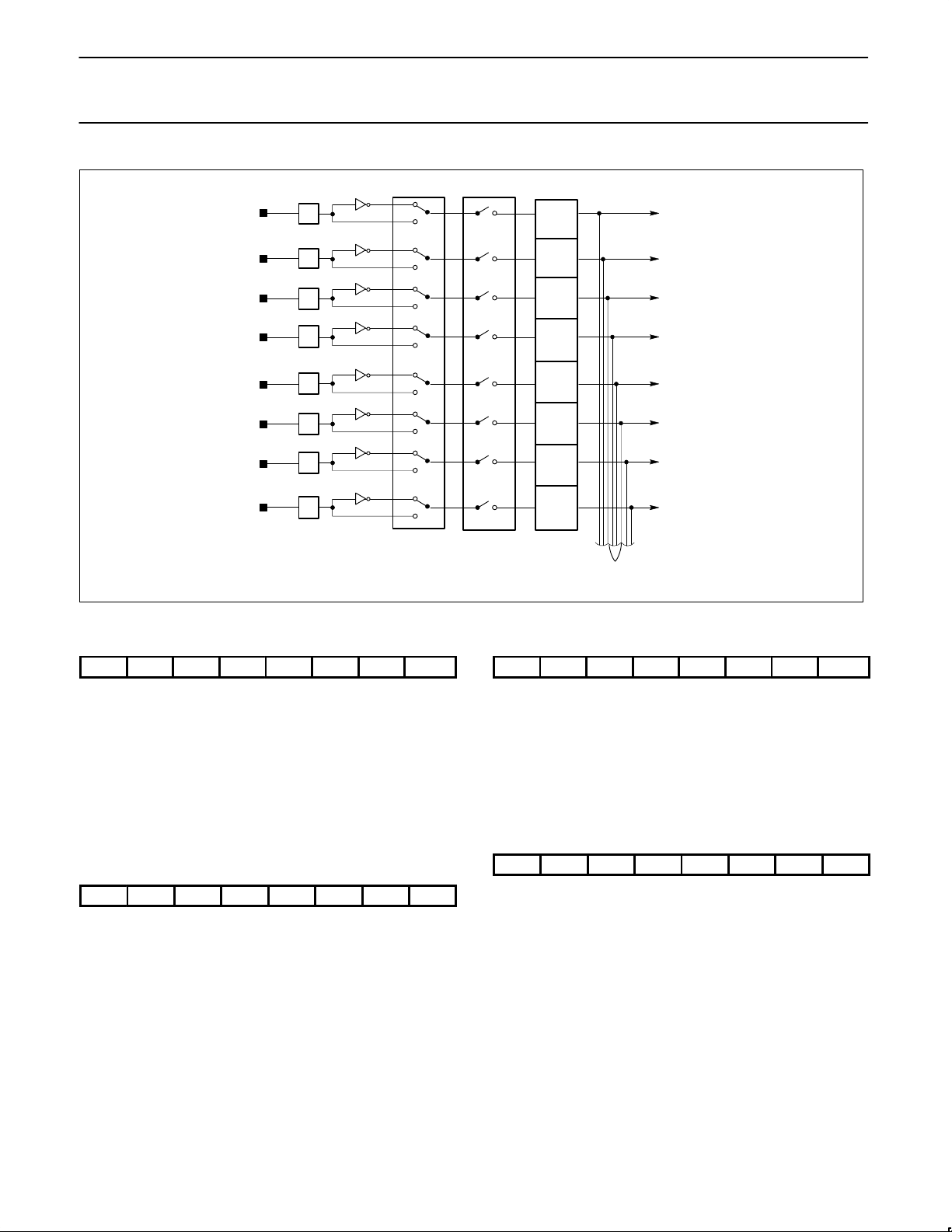
1.6.1 External Interrupts INT2/INT9
Port 1 lines serve an alternative purpose as eight additional
interrupts INT2 to INT9. When enabled, each of these lines may
“wake-up” the device from Power-down mode. Using the IX1
register, each pin may be initialized to either active HIGH or LOW.
IRQ1 is the interrupt request flag register. Each flag, if the interrupt
is enabled, will be set on an interrupt request but must be cleared by
software, i.e. via the interrupt software or when the interrupt is
disabled.
The Port 1 interrupts are level sensitive. A Port 1 interrupt will be
recognized when a level (HIGH or LOW depending on Interrupt
Polarity Register IX1) on P1x is held active for at least one machine
cycle. The Interrupt Request is not served until the next machine
cycle.
REGISTERS
IP0/1
PRIORITY
HIGH
LOW
X5
T0
X6
X1
X2
X7
T1
X3
X8
X4
X9
GLOBAL ENABLE
INTERRUPT POLLING SEQUENCE
Figure 11. Interrupt System
January 1995
19
Page 20
Philips Semiconductors Product specification
80CL31/80CL51Low-voltage single-chip 8-bit microcontrollers
IX1 IEN1 IRQ1
P1.7
X9
P1.6
P1.5
P1.4
P1.3
P1.2
P1.1
P1.0
Figure 12. External Interrupt Configuration
Interrupt enable register IEN0, IEN1
IEN0 (A8H)
EA - ES1 ES0 ET1 EX1 ET0 EX0
Bit Symbol Function
IEN0.7 EA General enable/disable control
0 = no interrupt is enabled
1 = any individually enabled interrupt will be accepted
IEN0.6 - Unused
IEN0.5 ES1 Unused
IEN0.4 ES0 Enable UAR T SIO interrupt
IEN0.3 ET1 Enable timer T1 interrupt
IEN0.2 EX1 Enable external interrupt
IEN0.1 ET0 Enable Timer T0 interrupt
IEN0.0 EX0 Enable external interrupt 0
IEN1 (E8H)
EX9 EX8 EX7 EX6 EX5 EX4 EX3 EX2
Bit Symbol Function
IEN1.7 EX9 Enable external interrupt 9
IEN1.6 EX8 Enable external interrupt 8
IEN1.5 EX7 Enable external interrupt 7
IEN1.4 EX6 Enable external interrupt 6
IEN1.3 EX5 Enable external interrupt 5
IEN1.2 EX4 Enable external interrupt 4
IEN1.1 EX3 Enable external interrupt 3
IEN1.0 EX2 Enable external interrupt 2
where 0 = interrupt disabled
1= interrupt enabled
X8
X7
X6
X5
X4
X3
X2
WAKE-UP
Interrupt priority register IP0, IP1
IP0 (B8H)
- - PS1 PS0 PT1 PX1 PT0 PX0
Bit Symbol Function
IP0.7 - Unused
IP0.6 - Unused
IP0.5 PS1 Unused
IP0.4 PS0 UART SIO interrupt
IP0.3 PT1 Timer 1 interrupt priority level
IP0.2 PX1 External interrupt 1 priority level
IP0.1 PT0 Timer 0 interrupt priority level
IP0.0 PX0 External interrupt 0 priority level
IP1 (B8H)
PX9 PX8 PX7 PX6 PX5 PX4 PX3 PX2
Bit Symbol Function
IP1.7 PX9 External interrupt 9 priority level
IP1.6 PX8 External interrupt 8 priority level
IP1.5 PX7 External interrupt 7 priority level
IP1.4 PX6 External interrupt 6 priority level
IP1.3 PX5 External interrupt 5 priority level
IP1.2 PX4 External interrupt 4 priority level
IP1.1 PX3 External interrupt 3 priority level
IP1.0 PX2 External interrupt 2 priority level
Interrupt priority is as follows:
0 = low priority
1 = high priority
January 1995
20
Page 21
Philips Semiconductors Product specification
80CL31/80CL51Low-voltage single-chip 8-bit microcontrollers
Interrupt polarity register IX1
IX1 (E9H)
IL9 IL8 IL7 IL6 IL5 IL4 IL3 IL2
Bit Symbol Function
IX1.7 IL9 External interrupt 9 polarity level
IX1.6 IL8 External interrupt 8 polarity level
IX1.5 IL7 External interrupt 7 polarity level
IX1.4 IL6 External interrupt 6 polarity level
IX1.3 IL5 External interrupt 5 polarity level
IX1.2 IL4 External interrupt 4 polarity level
IX1.1 IL3 External interrupt 3 polarity level
IX1.0 IL2 External interrupt 2 polarity level
Interrupt request flag register IRQ1
IRQ1 (C0H)
IQ9 IQ8 IQ7 IQ6 IQ5 IQ4 IQ3 IQ2
Bit Symbol Function
IRQ1.7 IQ9 External interrupt 9 request flag
IRQ1.6 IQ8 External interrupt 8 request flag
IRQ1.5 IQ7 External interrupt 7 request flag
IRQ1.4 IQ6 External interrupt 6 request flag
IRQ1.3 IQ5 External interrupt 5 request flag
IRQ1.2 IQ4 External interrupt 4 request flag
IRQ1.1 IQ3 External interrupt 3 request flag
IRQ1.0 IQ2 External interrupt 2 request flag
1.6.2 Interrupt Vectors
Vector Source
X0 0003H External 0
S0 0023H UART SIO
X5 0053H External 5
T0 000BH Timer 0
X6 005BH External 6
X1 0013H External 1
X2 003BH External 2
X7 0063H External 7
T1 001BH Timer 1
X3 0043H External 3
X8 006BH External 8
X4 004BH External 4
X9 0073H External 9
Interrupt priority
Each interrupt priority source can be set to either high or low priority.
If both priorities are requested simultaneously, the controller will
branch to the high priority vector.
A low priority interrupt can only be interrupted by a high priority
interrupt. A high priority interrupt routine cannot be interrupted.
1.6.3 Related registers
The following registers are used in conjunction with the interrupt
system:
Register Function
IX1 Interrupt polarity register
IRQ1 Interrupt enable register
IEN1 Interrupt enable register (INT2-INT9)
IP0 Interrupt priority register
IP1 Interrupt priority register (INT2-INT9)
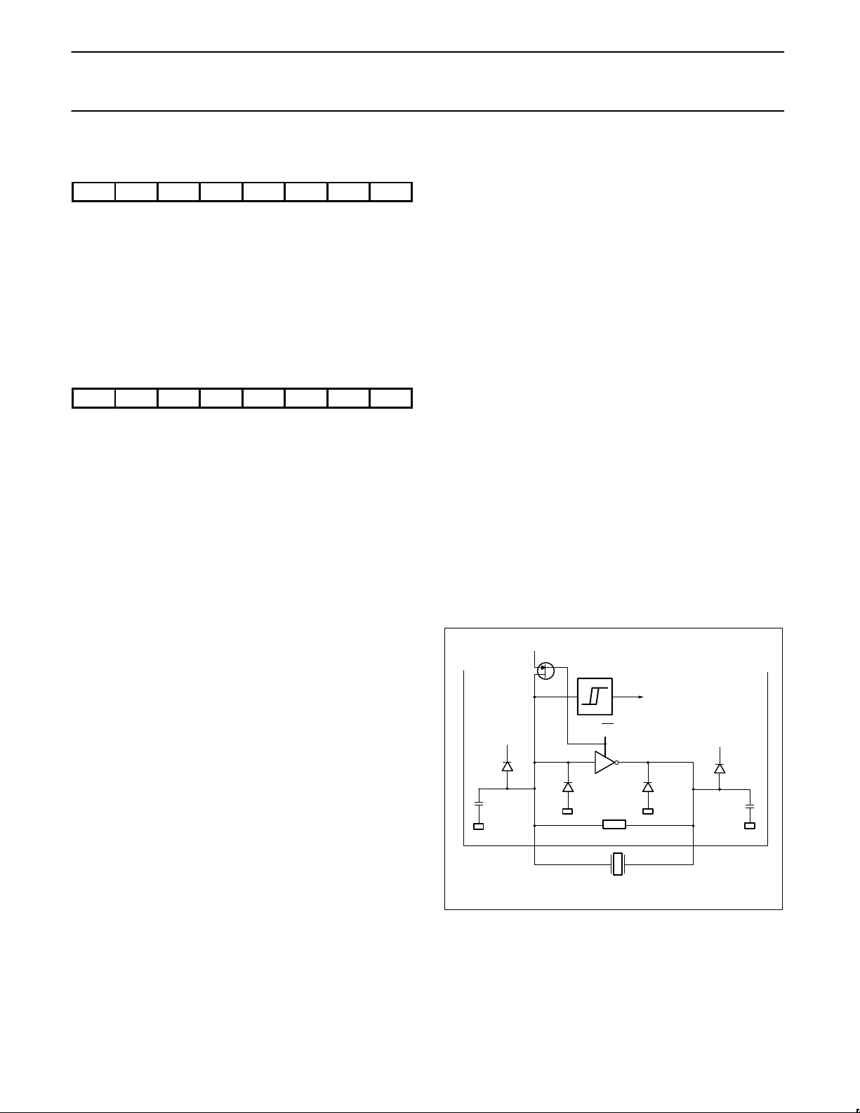
1.7 Oscillator registers
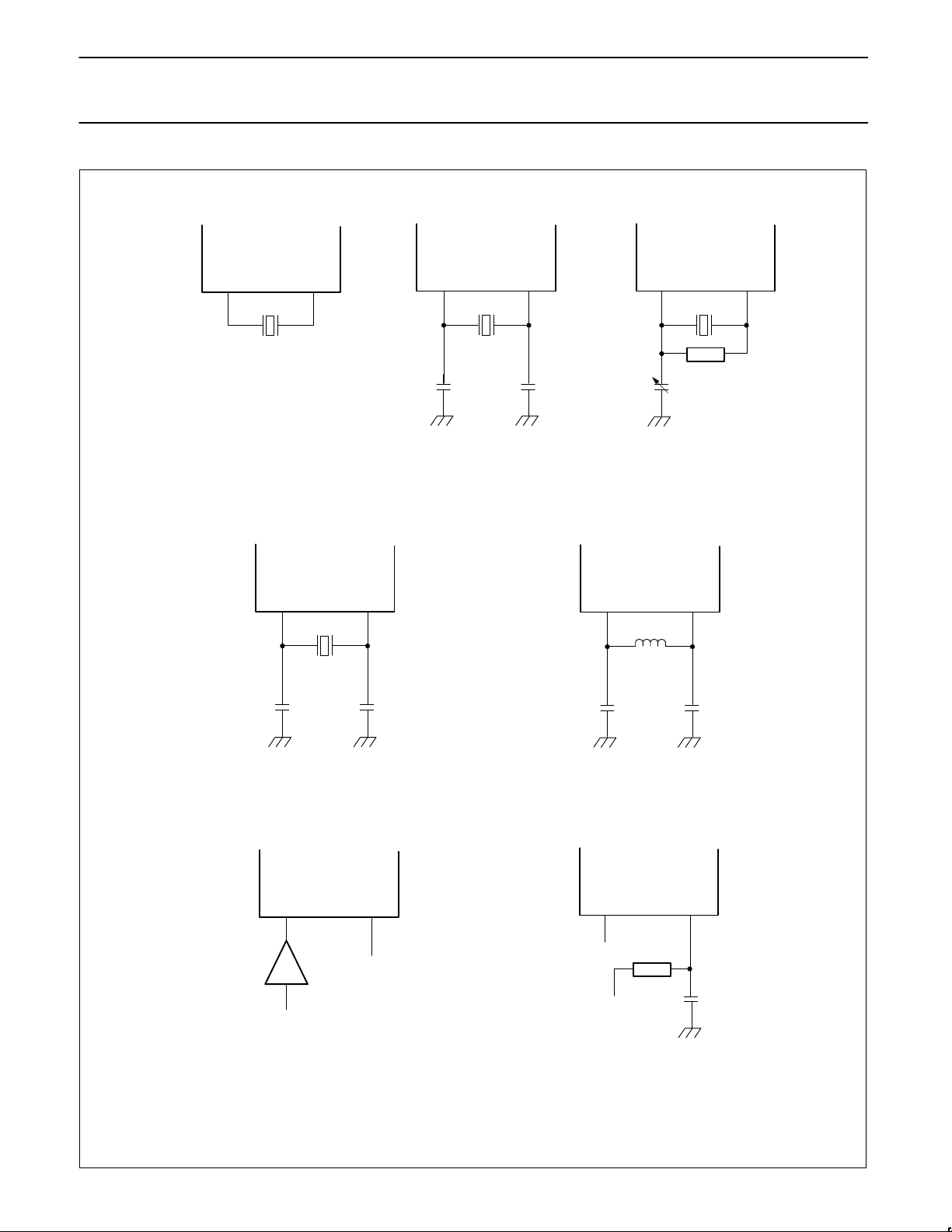
The on-chip circuitry of the 80CL51 is a single-stage inverting
amplifier biased by an internal feedback resistor (Figure 13). For
operation as standard quartz oscillator, no external components are
needed except at 32 KHz. When using external capacitors, ceramic
resonators, coils and RC networks to drive the oscillator, five
different configurations are supported (see Figure 14 and oscillator
options).
In the Power-down mode the oscillator is stopped XTAL1 is pulled
HIGH. The oscillator inverter is switched off to ensure no current will
flow regardless of the voltage at XTAL1. To drive the device with an
external clock source, apply the external clock signal to XTAL1, and
leave XTAL2 to float, as shown in Figure 14(f). There are no
requirements on the duty cycle of the external clock, since the input
to the internal clocking circuitry is split sing a flip-flop.
The following options are provided for optimum on-chip oscillator
performance. Please state option when ordering
1.7.1 Oscillator options (see Figure 14)
The following options are provided for optimum on-chip oscillator
performance. Please state option when ordering.
Osc.1: Figure 14(c): An option for 32 kHz clock applications with
external trimmer for frequency adjustment. A 4.7 MQ bias
resistor is needed for use in parallel with the crystal.
Osc. 2: Figure 14(e): An option for low-power, low-frequency
operations using LC components.
Osc. 3: An option for medium frequency range applications.
Osc. 4: An option for high frequency range applications.
RC: Figure 14(g): An option for an RC oscillator.
V
DD
80CL51
V
DD
C
1i
XTAL1 XTAL2
PD
R
bias
Figure 13. Oscillator
.
TO INTERNAL
TIMING CIRCUITS
V
DD
C
2i
January 1995
21
Page 22
Philips Semiconductors Product specification
80CL31/80CL51Low-voltage single-chip 8-bit microcontrollers
QUARTZ OSCILLATOR
STANDARD QUARTZ
OSCILLATOR
XTAL1 XTAL2 XTAL1 XTAL2 XTAL1 XTAL2
(a) (b) (c)
WITH EXTERNAL
CAPACITORS
32 kHz OSCILLATOR
LC-OSCILLATORCERAMIC RESONATOR
XTAL1 XTAL1
(d) (e)
RC-OSCILLATOREXTERNAL CLOCK
XTAL1 XTAL2 XTAL1 XTAL2
N.C.
N.C.
V
DD
January 1995
(f) (g)
Figure 14. Alternative Oscillator Configurations
22
Page 23
Philips Semiconductors Product specification
pp
pp
80CL31/80CL51Low-voltage single-chip 8-bit microcontrollers
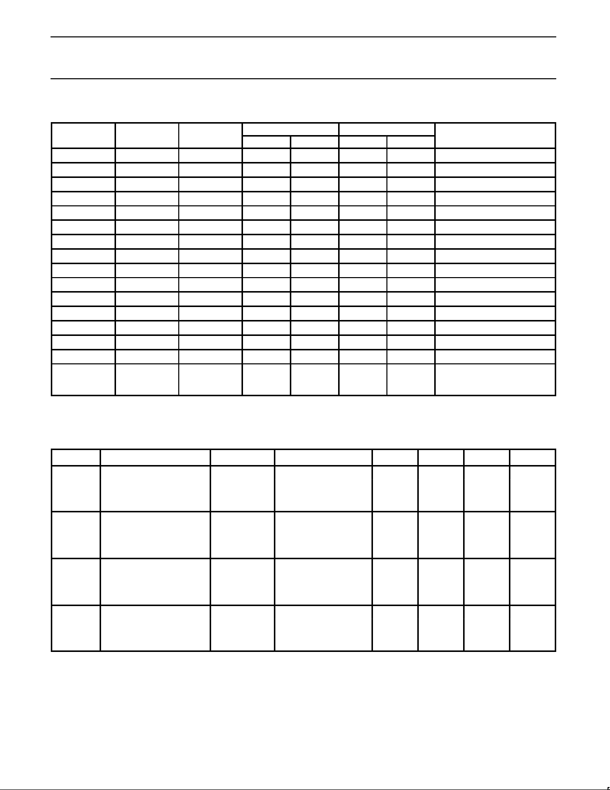
OSCILLATOR TYPE SELECTION GUIDE
C1 EXT. (pF) C2 EXT. (pF) MAX. RESONATOR
RESONATOR f(MHz) OPTION MIN. MAX. MIN. MAX. SERIES RESIST ANCE
Quartz 0.032 OSC. 1 0 0 5 15 15 kΩ
Quartz 1.0 OSC. 2 0 30 0 30 600 Ω
Quartz 3.58 OSC. 2 0 15 0 15 100 Ω
Quartz 4.0 OSC. 2 0 20 0 20 75 Ω
Quartz 6.0 OSC. 3 0 10 0 10 60 Ω
Quartz 10.0 OSC. 4 0 15 0 15 60 Ω
Quartz 12.0 OSC. 4 0 10 0 10 40 Ω
Quartz 16.0 OSC. 4 0 15 0 15 20 Ω
PXE 0.455 OSC. 2 40 50 40 50 10 Ω
PXE 1.0 OSC. 2 15 50 15 50 100 Ω
PXE 3.58 OSC. 2 0 40 0 40 10 Ω
PXE 4.0 OSC. 2 0 40 0 40 10 Ω
PXE 6.0 OSC. 2 0 20 0 20 5 Ω
PXE 10.0 OSC. 3 0 15 0 15 6 Ω
PXE 12.0 OSC. 4 10 40 10 40 6 Ω
LC OSC. 2 20 90 20 90 10 µH = 1 Ω
NOTES:
1. 32 kHz quartz crystals with a series resistance higher than 15 kΩ will reduce the guaranteed supply voltage range to 2.5 -3.5V .
2. The equivalent circuit data of the internal oscillator compares with that of matched crystals.
1
100 µH = 5 Ω
1 mH = 75 Ω
OSCILLATOR EQUIVALENT CIRCUIT PARAMETERS (SEE FIGURE 15)
SYMBOL P ARAMETER OPTION CONDITION MIN. TYP. MAX. UNIT
g
g
g
g
C1
C1
C1
C1
C2
C2
C2
C2
m
m
m
m
i
i
i
i
i
i
i
i
Transconductance
Input Capacitance
Output Capacitance
R2 Output Capacitance Osc.1 - 3800 - kΩ
R2 Osc. 2 - 65 - kΩ
R2 Osc. 3 - 18 - kΩ
R2 Osc. 4 - 5.0 - kΩ
Osc.1 T = +25 °C; VDD = 4.5V - 15 - µs
Osc.2 T = +25 °C; VDD = 4.5V 200 600 1000 µs
Osc.3 T = +25 °C; VDD = 4.5V 400 1500 4000 µs
Osc.4 T = +25 °C; VDD = 4.5V 1000 4000 10000 µs
Osc.1 - 3.0 - pF
Osc. 2 - 8.0 - pF
Osc. 3 - 8.0 - pF
Osc. 4 - 8.0 - pF
Osc.1 - 23 - pF
Osc. 2 - 8.0 - pF
Osc. 3 - 8.0 - pF
Osc. 4 - 8.0 - pF
January 1995
23
Page 24
Philips Semiconductors Product specification
80CL31/80CL51Low-voltage single-chip 8-bit microcontrollers
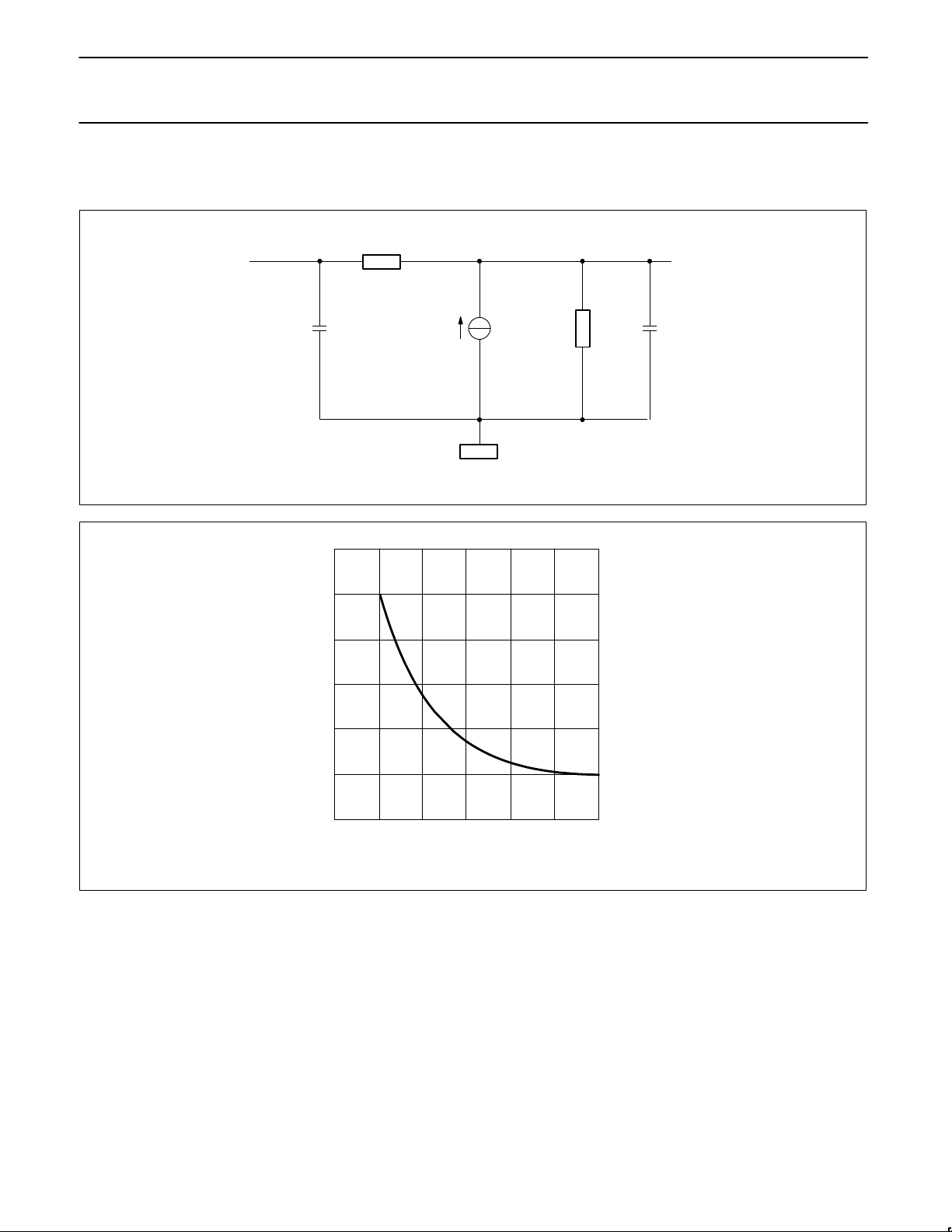
1.7.2 RC Oscillator (see Figure 16)
The externally adjustable RC-oscillator has a frequency range from 100 kHz to 500 kHz.
R
XTAL1
f
XTAL2
fosc
(kHz)
600
400
200
C1
i
SCHMITT
TRIGGER
V
1
g
m
Figure 15. Equivalent Circuit Diagram
R
2
C2
i
January 1995
0
02 4 6
RC(µs)
Figure 16. Frequency as a Function of RC
24
Page 25
Philips Semiconductors Product specification
80CL31/80CL51Low-voltage single-chip 8-bit microcontrollers
1.8 Reset Circuitry
To initialize the 80CL51, a reset is performed by either of two
methods:
– via the RST pin
– via a power-on-reset
It leaves the internal registers as follows:
REGISTER CONTENT
ACC 0000 0000
B 0000 0000
DPL 0000 0000
DPH 0000 0000
IEN0 0000 0000
IEN1 0000 0000
IP0 XX00 0000
IP1 0000 0000
IX1 0000 0000
IRQ1 0000 0000
PCH 0000 0000
PCL 0000 0000
PCON 0XXX 0000
PSW 0000 0000
P0-P3 1111 1111
S0BUF XXXX XXXX
S0CPN 0000 0000
SP 0000 0111
TCON 0000 0000
TH0, TH1 0000 0000
TL0, TH1 0000 0000
TL0, TL1 0000 0000
TMOD 0000 0000
The reset state of the port pins is mask- programmable and can
therefore be defined by the user.
The standard reset value for port P0-P3 is 111 1 11 11.
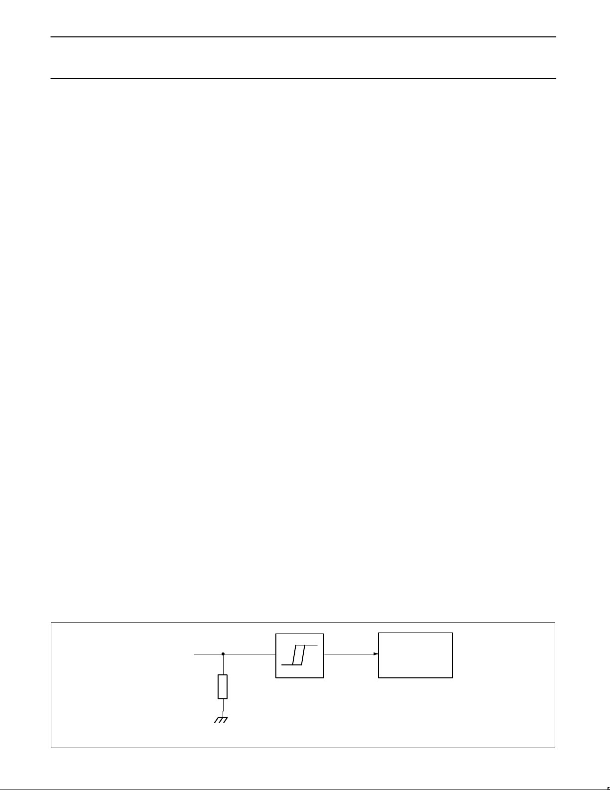
The reset input to the 80CL51 is RST pin 9. A Schmitt trigger
qualifies the input for noise rejection. The output of the Schmitt
trigger is sampled by the reset circuitry every machine cycle.
A reset is accomplished by holding the RST pin HIGH for at least
two machine cycles (24 oscillator periods), while the oscillator is
running. The CPU responds by generating an internal reset. Port
pins adopt their reset state immediately after RST goes HIGH.
During reset ALE and PSEN are held HIGH.
The external reset is asynchronous to the internal clock. The RST
pin is sampled during State 5, Phase 2 of every machine cycle. After
a HIGH is detected at the RST pin, an internal reset is repeated
every cycle until RST goes LOW.
The internal RAM is not affected by reset. When V
the RAM contents are indeterminate.
1.8.1 Power-on reset
The 80CL51 contains on-chip circuitry which switch the port pins to
the customer defined logic level as soon as V
1.3V. As soon as the minimum supply voltage is reached, the
oscillator will start up. However, to ensure that the oscillator is stable
before the controller starts, the clock signals are gated away from
the CPU for a further 1536 oscillator periods. During that time the
CPU is held in a reset state.
A hysteresis of approximately 50 mV at a typical power-on switching
level of 1.3 V will ensure correct operation.
The on-chip Power-on circuitry can be switched off via the mask
option “OFF”. This option reduces the power-down current to
typically 800µA and can be chosen if external reset circuitry is used.
For applications not requiring the internal reset option, “OFF” should
be chosen.
An automatic reset can be obtained at power-on by connecting the
RST pin to V
the RST pin is equal to V
decreases from V
internal resistor R
slowly V
of the Schmitt trigger long enough to effect a complete reset. The
time required is the oscillator start-up time, plus 2 machine cycles.
via a 10µF capacitor. At power-on, the voltage on
DD
decreases V
RST
DD
RST
minus the capacitor voltage, and
DD
as the capacitor discharges through the
to ground. The larger the capacitor, the more
must remain above the lower threshold
RST
exceeds
DD
is turned on
DD
1.9 P80CL31: ROMless version of P80CL51
The P80CL31 is a low voltage ROMless version of the P80CL51
microcontroller. The mask options on the P80CL31 are fixed as
follows:
• Port options: all ports have option “1S”, i.e., standard port, high
after reset
• Oscillator option: OSC3
• Power-on Reset option: OFF
1.10 P80C51: 5V standard version
The P80C51 is a 5V version of the low voltage P80CL51
microcontroller. All functional features of the P80CL51 are
maintained in the P80C51 with the exception of the mask options.
The mask options on the P80C51 are as follows:
• Port options: all ports have option “1S”, i.e., standard port, high
after reset.
• Oscillator options: OSC3
• Power-on Reset option: OFF
January 1995
RST
SCHMITT
TRIGGER
Figure 17. Reset Configuration at RST Pin
25
RESET
CIRCUITRY
Page 26
Philips Semiconductors Product specification
80CL31/80CL51Low-voltage single-chip 8-bit microcontrollers
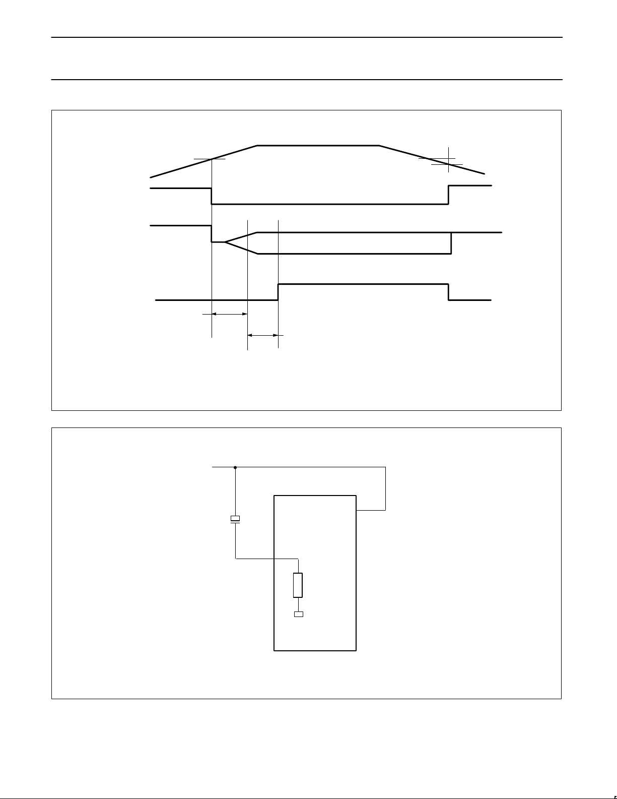
SWITCHING LEVEL
POR
SUPPLY
VOLTAGE
POWER-ON
RESET (INTERNAL)
OSCILLATOR
CPU RUNNING
START-UP
TIME
1536 OSCILLATOR
PERIODS DELAY
HYSTERESIS
Figure 18. Power-on Reset Switching Level
V
CC
+
10µF
80CL51
RST
R
RST
V
CC
January 1995
Figure 19. Recommended Power-on Reset Circuitry
26
Page 27
Philips Semiconductors Product specification
IILI
3)
I
Input current logic 1 to 0 transition
IOLOutput sink
LOW
I
Output source current HIGH
80CL31/80CL51Low-voltage single-chip 8-bit microcontrollers
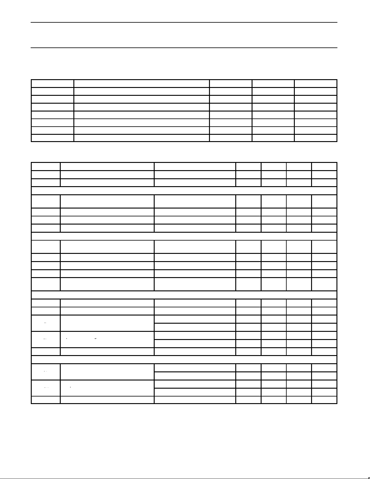
2.0 RATINGS
Limiting values in accordance with the Absolute Maximum System (IEC 134)
SYMBOL
V
V
II, I
P
T
T
T
DD
I
O
TOT
STG
AMB
J
Supply voltage (pin 40) -0.5 + 6.5 V
All input voltages -0.5 VDD+0.5 V
DC current into any input or output - 5 mA
Total power dissipation - 300 mW
Storage temperature range -65 +150 °C
Operating ambient temperature range -40 +85 °C
Operating junction temperature - 125 °C
3.0 DC CHARACTERISTICS P80CL31/P80CL51
VSS = 0V; T
SYMBOL
V
DD
V
DD
Supply current operating (Note 1, Note 4)
I
DD
I
DD
I
DD
I
DD
Idle Mode (Note 2, Note 4)
I
DD
I
DD
I
DD
I
DD
I
PD
Inputs
V
IL
V
IH
TL
+/I
IL
Outputs
-
OH
R
RST
NOTES:
1. The operating supply current is measured with all output pins disconnected; XTAL 1 driven with t
XTAL 2 not connected; EA = RST = Port 0 = V
2. The idle mode supply current is measured with all output pins disconnected; XTAL 1 driven with t
connected; EA = Port 0 = V
3. The power-down current is measured with all output pins disconnected; XTAL 1 not connected; EA = Port 0 = VDD; RST = VSS; all open
drain outputs connected to V
4. Circuits with Power-on Reset option “OFF” are tested at VDD minimum = 1.8V; with option “ON” (typically 1.3V) they are tested at V
minimum = 2.3V. Please note, option “ON” is only available on P80CL51.
= -40 to +85°C; all voltages with respect to VSS unless otherwise specified.
AMB
PARAMETER CONDITIONS MIN. TYP. MAX. UNIT
Supply voltage V
RAM retention in power down mode 1.0 – – V
OSC 1 option f
OSC 2 option f
OSC 3 option f
OSC 4 option f
OSC 1 option f
OSC 2 option f
OSC 3 option f
OSC 4 option f
Power down (Note 3, Note 4) V
Input voltage LOW V
Input voltage HIGH 0.7V
nput current logic 0 (Port 1, 2,
Input current logic 1 to 0 transition
(Port 1, 2, 3)
Input leakage current (Port 0, EA) V
current
Output source current HIGH
(push-pull options only)
RST pull-down resistor 10 – 200 kΩ
; RST = VSS; all open drain outputs connected to V
DD
SS.
PARAMETER MIN. MAX. UNIT
= 0V 1.8 - 6.0 V
SS
= 32 KHz; VDD = 1.8V
cIk
- 25°C
T
AMB
= 3.58 MHz; VDD = 3V - - 2.5 mA
cIk
= 16 MHz; VDD = 5V - - 24 mA
cIk
= 16 MHz; VDD = 5V - - 26 mA
cIk
= 32 KHz; VDD = 1.8V
cIk
= 25°C
T
AMB
= 3.58 MHz; VDD = 3V - - 1.0 mA
cIk
= 16 MHz; VDD = 5V - - 10 mA
cIk
= 16 MHz; VDD = 5V - - 12 mA
cIk
= 1.8V ,
DD
= 25°C
T
AMB
V
= 5V, V
DD
V
= 2.5V , V
DD
V
= 5V, V
DD
V
= 2.5V , V
DD
< V
SS
V
= 5V, V
DD
V
= 2.5V , V
DD
V
= 5V; V
DD
V
= 2.5V; V
DD
; all open drain outputs connected to VSS.
DD
= 0.4V
IN
= 0.4V
IN
= VDD/2 - - 1.0 mA
IN
= VDD/2 - - 500 µA
IN
< V
I
DD
= 0.4V 1.6 - - mA
OL
= 0.4V 0.7 - - mA
OL
= V
OH
-0.4V 1.6 - - mA
DD
= V
OH
-0.4V 0.7 - - mA
DD
SS.
- - 50 µA
- - 25 µA
- 10 µA
SS
DD
-
-
- 0.3V
- V
DD
DD
- 100 µA
- 50 µA
- - 10 µA
= tf = 10ns; VIL = VSS; VIH = VDD;
r
= tf = 10ns; VIL = VSS. XTAL 2 not
r
V
V
DD
January 1995
27
Page 28
Philips Semiconductors Product specification
80CL31/80CL51Low-voltage single-chip 8-bit microcontrollers
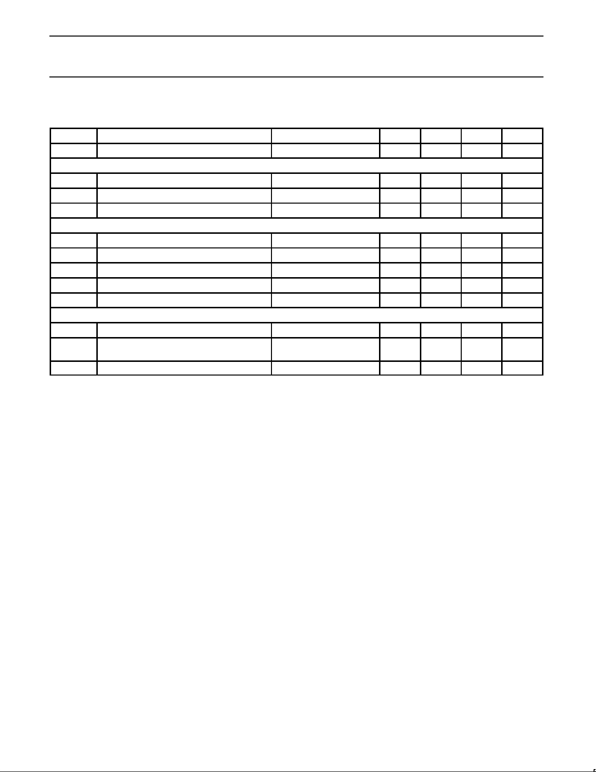
4.0 DC CHARACTERISTICS P80C51
VSS = 0V; VDD = 5V ± 10%; f
SYMBOL
V
Supply voltage V
DD
Supply Current
I
DD
I
DD
I
PD
Operating (Note 1) f
Idle mode (Note 2) f
Power down (Note 3) VDD = 5V – – 50 µA
Inputs
V
V
I
I
I
Input voltage LOW V
IL
Input voltage HIGH 0.7V
IH
Input current logic 0 (Port 1, 2, 3) VIN = 0.4V – – 100 µA
IL
Input current logic 1 to 0 transition (Port 1, 2, 3) VIN = VDD/2 – – 1.0 mA
IL
Input leakage current (Port 0, EA) VSS < VI < V
IL
Outputs
I
OL
I
OH
R
RST
Output sink current LOW VOL = 0.4V 1.6 – – mA
Output source current HIGH
(push-pull options only)
RST pull-down resistor 10 – 200 kΩ
NOTES:
1. The operating supply current is measured with all output pins disconnected; XTAL 1 driven with t
= VSS; VIH = VDD; XTAL 2 not connected; EA = RST = Port 0 = VDD; all open drain outputs connected to VSS.
V
IL
2. The idle mode supply current is measured with all output pins disconnected; XTAL 1 driven with t
= VSS. XTAL 2 not connected; EA = Port 0 = VDD; RST = VSS; all open drain outputs connected to V
V
IL
3. The power-down current is measured with all output pins disconnected; XTAL 1 not connected;
EA = Port 0 = V
4. Please note, option “ON” is only available on P80CL51.
; RST = VSS; all open drain outputs connected to VSS.
DD
= 3.5 to 16MHz; T
clk
= -40 to +85°C; all voltages with respect to VSS unless otherwise specified.
AMB
PARAMETER CONDITIONS MIN. TYP. MAX. UNIT
= 0V 4.5 - 5.5 V
SS
= 16MHz, VDD = 5V – – 24 mA
CLK
= 16MHz, VDD = 5V – – 10 mA
CLK
– 0.3V
– V
DD
DD
DD
SS
DD
– – 10 µA
VOH = VDD – 0.4V 1.6 – – mA
= tF = 10ns;
R
= tF = 10ns;
R
SS.
V
V
January 1995
28
Page 29
Philips Semiconductors Product specification
SYMBOL
PARAMETER
SYMBOL
PARAMETER
80CL31/80CL51Low-voltage single-chip 8-bit microcontrollers
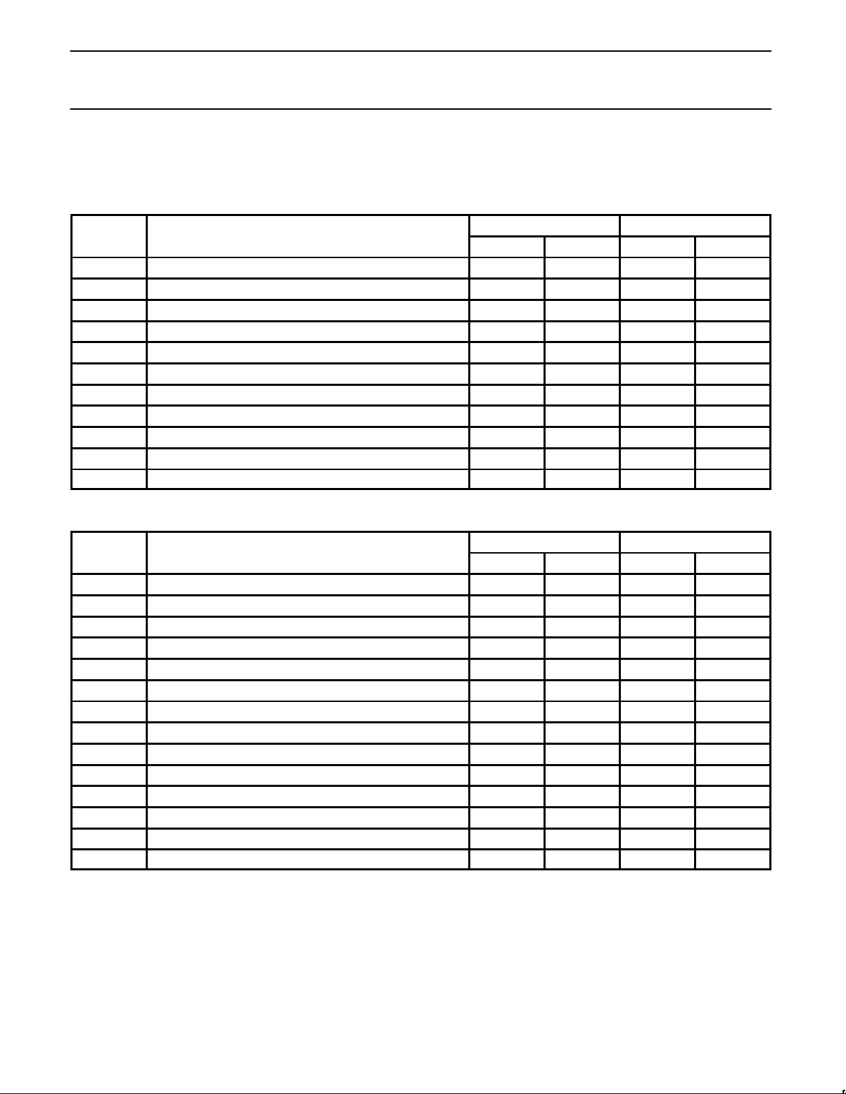
5.0 AC CHARACTERISTICS
VDD = 5 V; VSS = 0V; T
PROGRAM MEMORY (See Figure 20)
t
t
t
t
t
t
t
t
t
AFC
t
LL
AL
LA
LC
LIV
CC
CIV
t
CIF
AIV
CI
ALE pulse duration 2TCK-40 - - ns
Address set-up time to ALE TCK-40 - - ns
Address hold time to ALE TCK-35 - - ns
Time from ALE to control pulse PSEN TCK-25 - - ns
Time from ALE to valid instruction input - - 4TCK-100 ns
Control pulse duration PSEN 3TCK-35 - - ns
Time from PSEN to valid instruction input - - 3TCK-125 ns
Input instruction hold time after PSEN 0 - - ns
Input instruction float delay after PSEN - - TCK-20 ns
Address to valid instruction input - - 5TCK-115 ns
Address float time to PSEN 0 - - ns
= -40 to +85°C; CL = 50 pF for Port 0, ALE and PSEN; CL = 40pF for all other outputs, unless otherwise specified.
amb
VARIABLE CLOCK
MIN. TYP. MAX. UNIT
EXTERNAL DATA MEMORY (See Figures 21 and 22)
VARIABLE CLOCK
MIN. TYP. MAX. UNIT
t
RR
t
WW
t
LA
t
RD
t
DFR
t
LD
t
AD
t
LW
t
AW
t
WHLH
t
DWX
t
DW
t
WD
t
WAFR
NOTE:
1. Interfacing the 80CL51 or P80C51 to devices with float times up to 75ns is permitted. This limited bus connection will not cause damage to
Port 0 drivers.
RD pulse duration 6TCK-100 - - ns
WR pulse duration 6TCK-100 - - ns
Address hold time after ALE TCK-35 - - ns
RD to valid data input TCK-35 - 5TCK-165 ns
Data float delay after RD - - 2TCK-70 ns
Time from ALE to valid data input - - 8TCK-150 ns
Address to valid data input - - 9TCK-165 ns
Time from ALE to RD and WR 3TCK-50 - 3TCK+50 ns
Time from address to RD and WR 4TCK-130 - - ns
Time from RD or WR HIGH to ALE HIGH TCK-40 - TCK-40 ns
Data valid to WR transition TCK-60 - - ns
Data set-up time before WR TCK-150 - - ns
Data hold time after WR TCK-50 - - ns
Address float delay after RD (Note 1) - - 12 ns
January 1995
29
Page 30
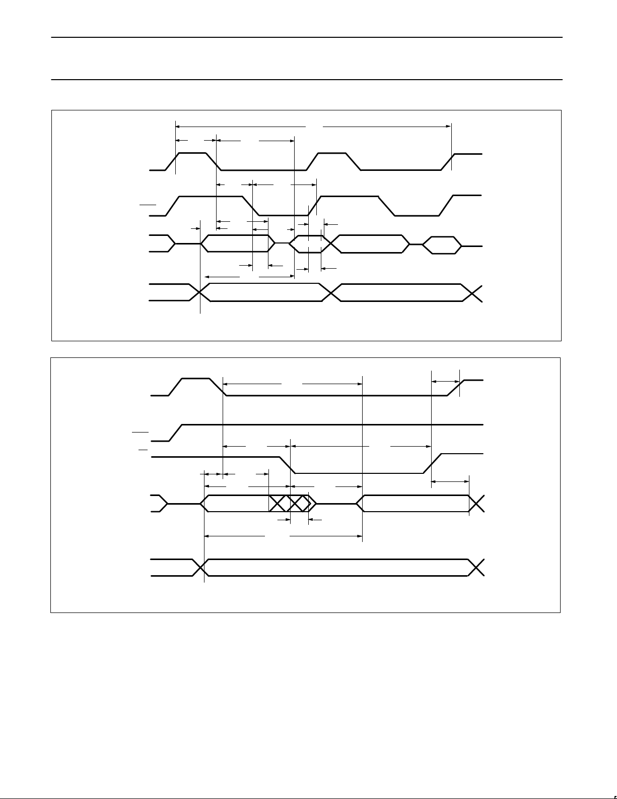
Philips Semiconductors Product specification
80CL31/80CL51Low-voltage single-chip 8-bit microcontrollers
t
CV
t
LIV
ALE
t
LL
PORT 0
PORT 2
ALE
PSEN
RD
PORT 0
PSEN
t
LC
t
t
AL
LA
AD0 TO AD7
t
AL
t
AIV
ADDRESS A8 TO A15 ADDRESS A8 TO A15
t
t
CIV
CC
INST. INPUT
t
CIF
AD0 TO AD7
t
CI
INST. INPUT
Figure 20. Read from Program Memory
t
t
LD
t
LW
t
AL
t
LA
t
AW
AD0 TO AD7
t
RD
t
AFR
t
AD
t
RR
DATA INPUT
WHLH
t
DFR
PORT2
January 1995
ADDRESS A8 TO A15 OR PORT 2 OUT
Figure 21. Read from Data Memory
30
Page 31
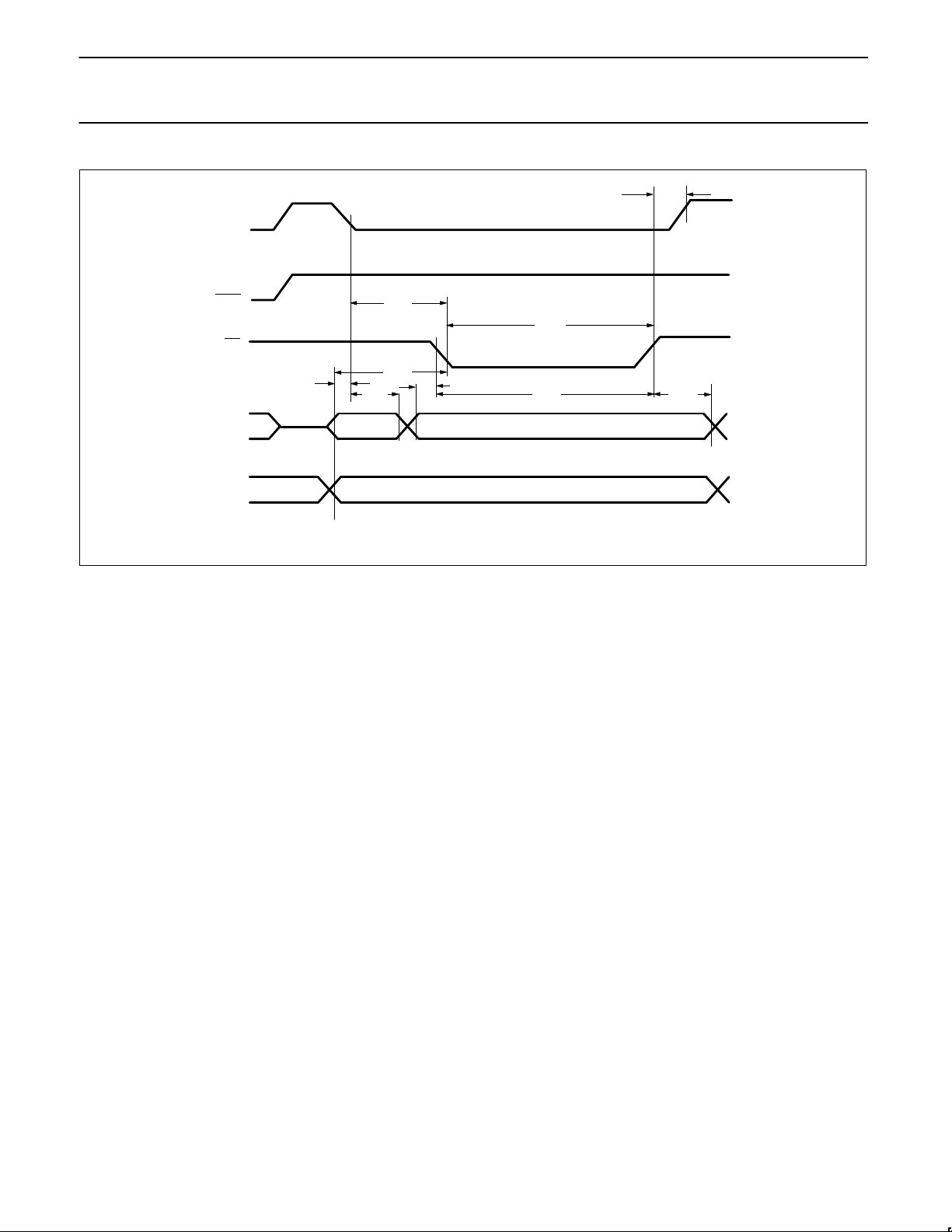
Philips Semiconductors Product specification
80CL31/80CL51Low-voltage single-chip 8-bit microcontrollers
t
WHLH
ALE
PSEN
WR
PORT 0
PORT2
t
LW
t
t
AL
AD0 TO AD7 DATA OUTPUT
AW
t
LA
t
WX
ADDRESS A8 TO A15 OR PORT 2 OUT
Figure 22. Write to Data Memory
t
t
WW
DW
t
WD
January 1995
31
Page 32
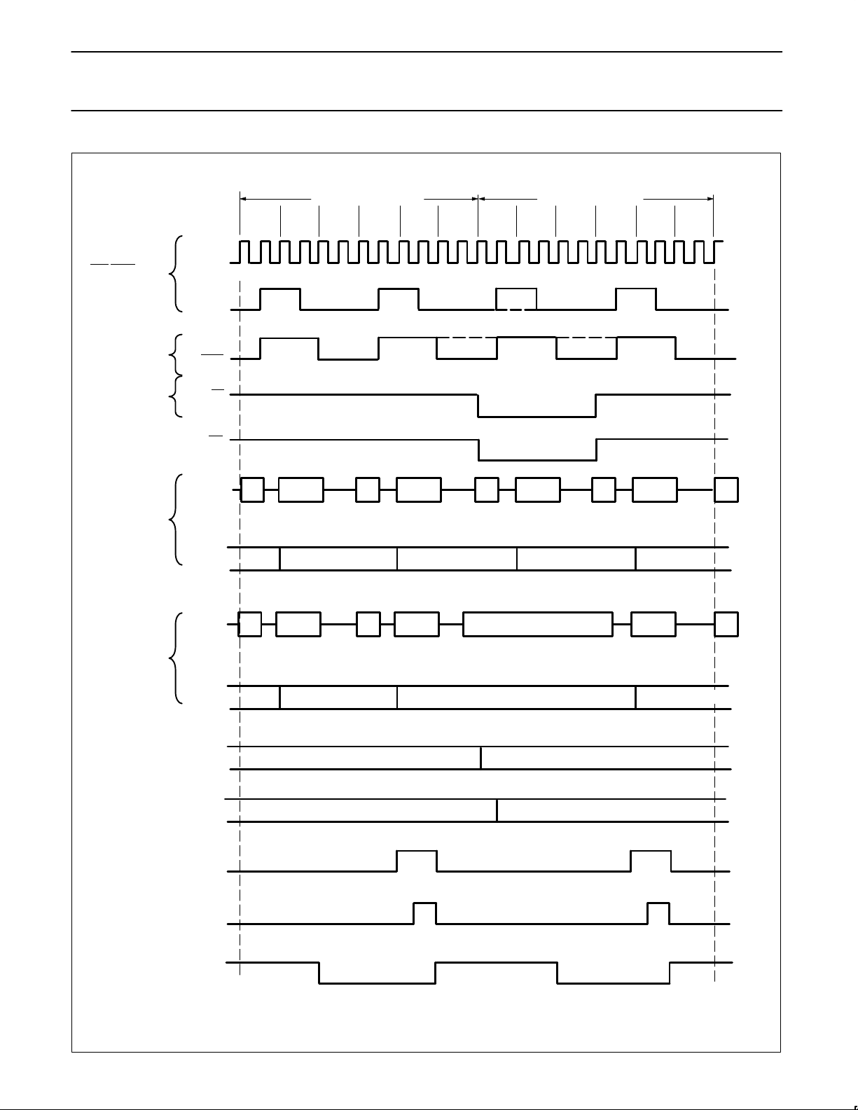
Philips Semiconductors Product specification
80CL31/80CL51Low-voltage single-chip 8-bit microcontrollers
ONE MACHINE CYCLE ONE MACHINE CYCLE
S1 S2 S3 S4 S5 S6 S6S5S4S3S2S1
P1 P2 P1 P2 P1 P2 P1 P2 P1 P2 P1 P2 P1 P2 P1 P2 P1 P2 P1 P2 P1 P2 P1 P2
XTAL1
DOTTED LINES
VALID WHEN
ARE
RD OR WR
ARE ACTIVE
ONLY ACTIVE
DURING A READ
FROM EXTERNAL
DATA MEMORY
ONLY ACTIVE
DURING A WRITE
TO EXTERNAL
DATA MEMORY
INPUT
ALE
PSEN
RD
WR
EXTERNAL
PROGRAM
MEMORY
FETCH
READ OR WRITE
OF EXTERNAL
DATA MEMORY
BUS
(PORT 0)
PORT 2
BUS
(PORT 0)
PORT 2
PORT 0,2,3
OUTPUT
PORT 1
OUTPUT
PORT 0,2,3
OUTPUT
INST
ADDRESS
IN
A0-A7
ADDRESS A8-A15 ADDRESS A8-A15 ADDRESS A8-A15 ADDRESS A8-A15
INSTINADDRESS
A0-A7
ADDRESS A8-A15
INST
ADDRESS
IN
INSTINADDRESS
OLD DATA NEW DATA
OLD DATA
A0-A7
A0-A7
SAMPLING TIME OF I/O PORT PINS DURING INPUT
INSTINADDRESS
DATA OUTPUT OR DATA INPUT
ADDRESS A8-A15 OR PORT 2 OUT
A0-A7
INSTINADDRESS
NEW DATA
A0-A7
ADDRESS
A0-A7
ADDRESS A8-A15
PORT 1
OUTPUT
SERIAL
PORT
CLOCK
January 1995
Figure 23. Instruction Cycle Timing
32
Page 33
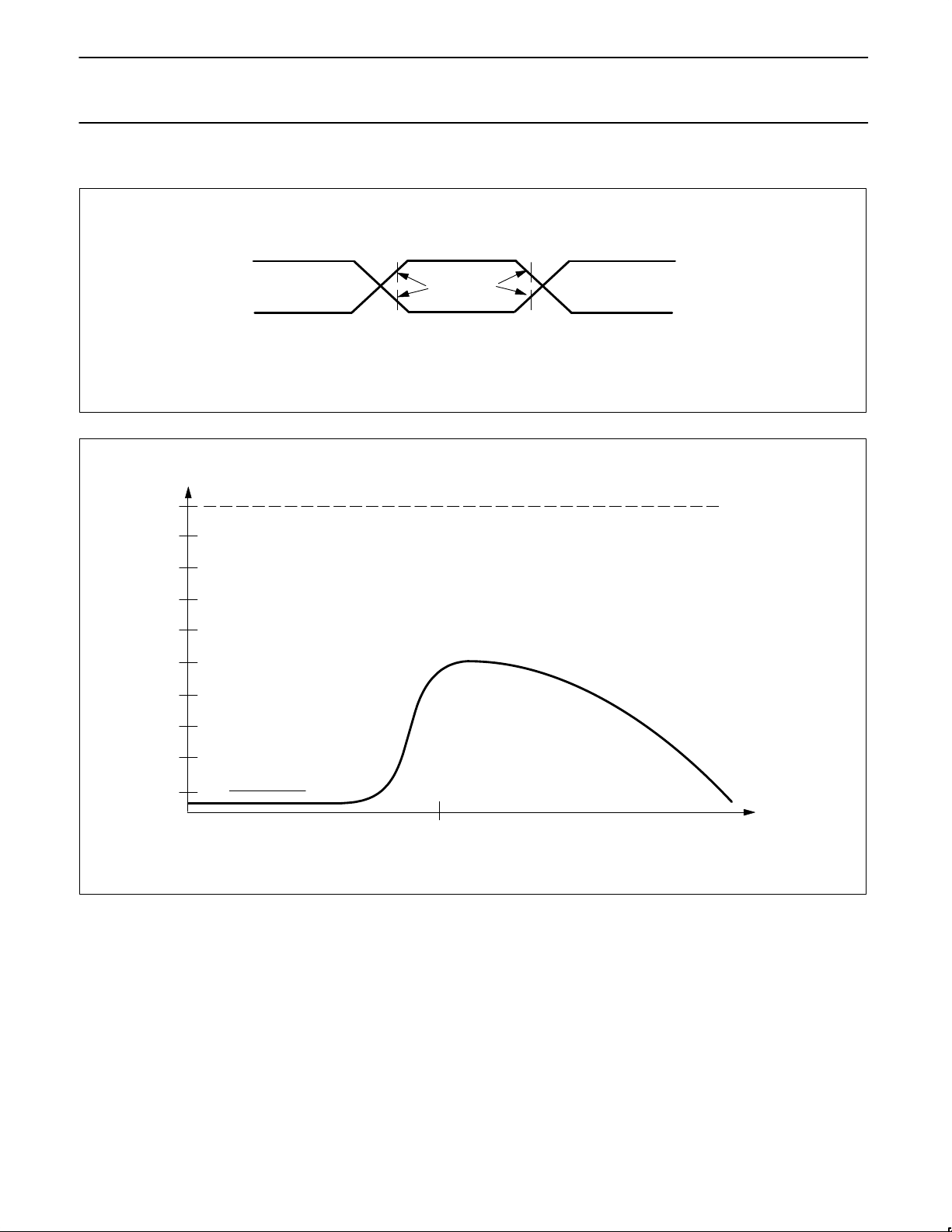
Philips Semiconductors Product specification
80CL31/80CL51Low-voltage single-chip 8-bit microcontrollers
6.0 CHARACTERISTICS CURVES
500µA
500µA
0.9V
0.4V
DD
DD
0.7V
0.3V
DD
TEST POINTS
DD
0.7V
0.3V
DD
DD
Figure 24. AC Testing Input Waveform
-I
L
I
TL
100µA
January 1995
I
IL
V
IN
2.5V
Figure 25. Input Current at VDD = 5V
33
Page 34
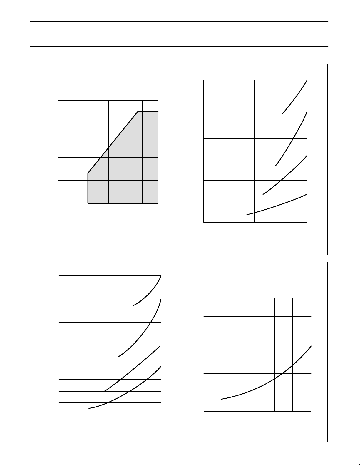
Philips Semiconductors Product specification
80CL31/80CL51Low-voltage single-chip 8-bit microcontrollers
20
16 MHz
18
16
14
12
f
XTAL
10
(MHz)
16
12 MHz
12
8
6
4
2
0
0246
(V)
V
DD
Figure 26. P80CL51/31 Frequency Operating Range
6
16 MHz
5
I
idle
(mA)
4
3
2
12 MHz
8 MHz
I
DD
8
(mA)
4
0
0246
(V)
V
DD
8 MHz
3.58 MHz
Figure 27. P80CL51/31 Typical Operating Current vs
I
PD
(µA)
Frequency and V
6
4
2
DD
, T
amb
= 25oC.
1
0
0246
Figure 28. P80CL51/31 Typical Idle Current vs
Frequency and V
January 1995
3.58 MHz
0
V
(V)
DD
024 6
(V)
V
DD
Figure 29. P80CL51/31 Typical Power-Down Current
DD
, T
amb
= 25oC.
vs Frequency and V
DD
, T
amb
= 25oC.
34
Page 35
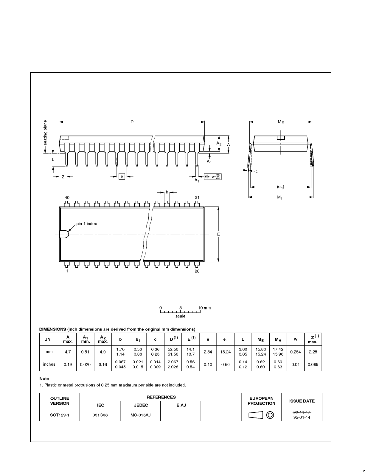
Philips Semiconductors Product specification
80CL31/80CL51Low-voltage single-chip 8-bit microcontrollers
DIP40: plastic dual in-line package; 40 leads (600 mil) SOT129-1
January 1995
35
Page 36
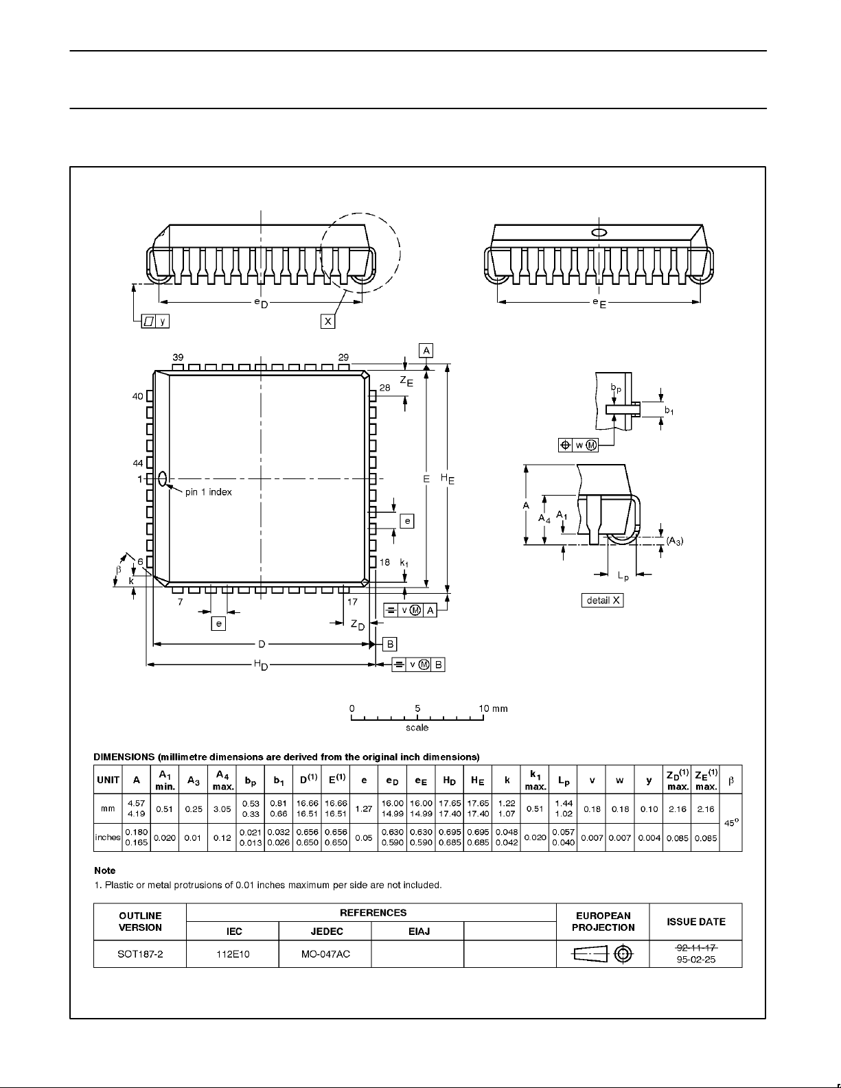
Philips Semiconductors Product specification
80CL31/80CL51Low-voltage single-chip 8-bit microcontrollers
PLCC44: plastic leaded chip carrier; 44 leads SOT187-2
January 1995
36
Page 37
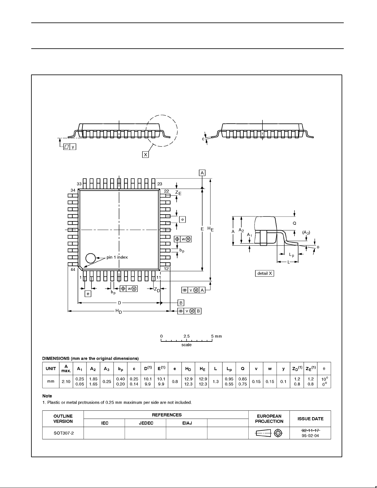
Philips Semiconductors Product specification
80CL31/80CL51Low-voltage single-chip 8-bit microcontrollers
QFP44: plastic quad flat package; 44 leads (lead length 1.3 mm); body 10 x 10 x 1.75 mm SOT307-2
January 1995
37
Page 38

Philips Semiconductors Product specification
80CL31/80CL51Low-voltage single-chip 8-bit microcontrollers
NOTES
January 1995
38
Page 39

Philips Semiconductors Product specification
80CL31/80CL51Low-voltage single-chip 8-bit microcontrollers
NOTES
January 1995
39
Page 40

Philips Semiconductors Product specification
80CL31/80CL51Low-voltage single-chip 8-bit microcontrollers
DEFINITIONS
Data Sheet Identification Product Status Definition
Objective Specification
Preliminary Specification
Product Specification
Formative or in Design
Preproduction Product
Full Production
Philips Semiconductors and Philips Electronics North America Corporation reserve the right to make changes, without notice, in the products,
including circuits, standard cells, and/or software, described or contained herein in order to improve design and/or performance. Philips
Semiconductors assumes no responsibility or liability for the use of any of these products, conveys no license or title under any patent, copyright,
or mask work right to these products, and makes no representations or warranties that these products are free from patent, copyright, or mask
work right infringement, unless otherwise specified. Applications that are described herein for any of these products are for illustrative purposes
only. Philips Semiconductors makes no representation or warranty that such applications will be suitable for the specified use without further testing
or modification.
LIFE SUPPORT APPLICA TIONS
Philips Semiconductors and Philips Electronics North America Corporation Products are not designed for use in life support appliances, devices,
or systems where malfunction of a Philips Semiconductors and Philips Electronics North America Corporation Product can reasonably be expected
to result in a personal injury. Philips Semiconductors and Philips Electronics North America Corporation customers using or selling Philips
Semiconductors and Philips Electronics North America Corporation Products for use in such applications do so at their own risk and agree to fully
indemnify Philips Semiconductors and Philips Electronics North America Corporation for any damages resulting from such improper use or sale.
Philips Semiconductors
811 East Arques Avenue
P.O. Box 3409
Sunnyvale, California 94088–3409
Telephone 800-234-7381
This data sheet contains the design target or goal specifications for product development. Specifications
may change in any manner without notice.
This data sheet contains preliminary data, and supplementary data will be published at a later date. Philips
Semiconductors reserves the right to make changes at any time without notice in order to improve design
and supply the best possible product.
This data sheet contains Final Specifications. Philips Semiconductors reserves the right to make changes
at any time without notice, in order to improve design and supply the best possible product.
Philips Semiconductors and Philips Electronics North America Corporation
register eligible circuits under the Semiconductor Chip Protection Act.
Copyright Philips Electronics North America Corporation 1995
All rights reserved. Printed in U.S.A.
 Loading...