

Page 1

INTEGRATED CIRCUITS
80C32/87C52
CMOS single-chip 8-bit microcontrollers
Product specification 1996 Aug 16
IC20 Data Handbook
Page 2

Philips Semiconductors Product specification
80C32/87C52CMOS single-chip 8-bit microcontrollers
DESCRIPTION
The Philips 80C32/87C52 is a high-performance microcontroller
fabricated with Philips high-density CMOS technology. The Philips
CMOS technology combines the high speed and density
characteristics of HMOS with the low power attributes of CMOS.
Philips epitaxial substrate minimizes latch-up sensitivity.
The 87C52 contains an 8k × 8 EPROM and the 80C32 is ROMless.
Both contain a 256 × 8 RAM, 32 I/O lines, three 16-bit
counter/timers, a six-source, two-priority level nested interrupt
structure, a serial I/O port for either multi-processor
communications, I/O expansion or full duplex UART, and on-chip
oscillator and clock circuits.
In addition, the 80C32/87C52 has two software selectable modes of
power reduction—idle mode and power-down mode. The idle mode
freezes the CPU while allowing the RAM, timers, serial port, and
interrupt system to continue functioning. The power-down mode
saves the RAM contents but freezes the oscillator, causing all other
chip functions to be inoperative.
See 80C52/80C54/80C58 datasheet for ROM device specifications.
FEA TURES
•80C51 based architecture
•8032 compatible
– 8k × 8 EPROM (87C52)
– ROMless (80C32)
– 256 × 8 RAM
– Three 16-bit counter/timers
– Full duplex serial channel
– Boolean processor
•Memory addressing capability
– 64k ROM and 64k RAM
•Power control modes:
– Idle mode
– Power-down mode
•CMOS and TTL compatible
•Three speed ranges:
– 3.5 to 16MHz
– 3.5 to 24MHz
– 3.5 to 33MHz
•Five package styles
•Extended temperature ranges
•OTP package available
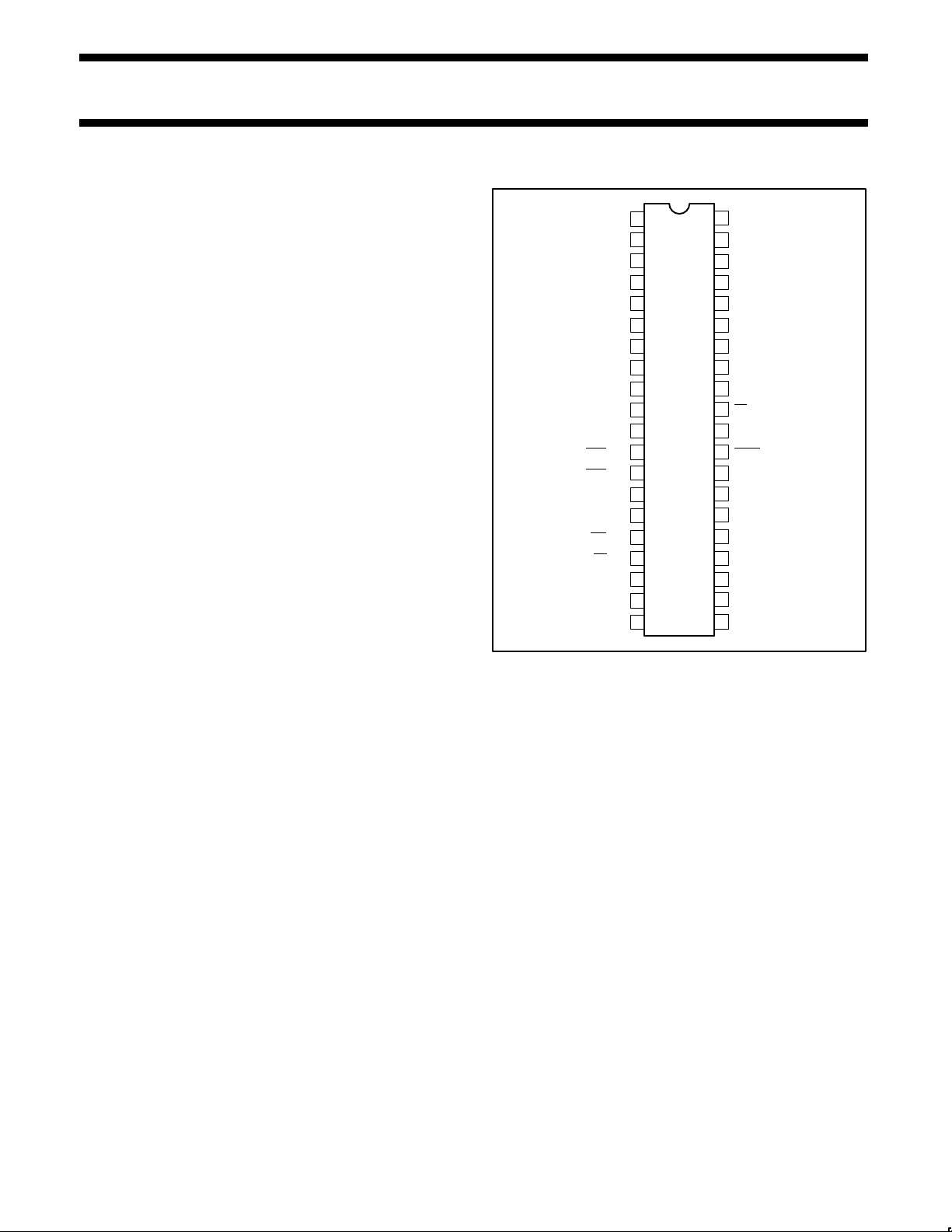
PIN CONFIGURATIONS
1
P1.0/T2
P1.2
P1.3
P1.4
P1.5
P1.6
P1.7
RST
/P3.2
/P3.3
T0/P3.4
T1/P3.5
/P3.6
/P3.7
XTAL2
XTAL1
V
2
3
4
5
6
7
8
9
10
11
12
13
14
15
16
17
18
19
20
SS
P1.1/T2EX
RxD/P3.0
TxD/P3.1
INT0
INT1
WR
RD
CERAMIC
AND
PLASTIC
DUAL
IN-LINE
PACKAGE
V
40
39
P0.0/AD0
38
P0.1/AD1
37
P0.2/AD2
36
P0.3/AD3
35
P0.4/AD4
34
P0.5/AD5
33
P0.6/AD6
32
P0.7/AD7
31
EA/V
30
ALE/PROG
29
PSEN
28
P2.7/A15
27
P2.6/A14
26
P2.5/A13
25
P2.4/A12
24
P2.3/A11
23
P2.2/A10
22
P2.1/A9
21
P2.0/A8
DD
PP
SU00060
1996 Aug 16 853–1562 17195
2
Page 3

Philips Semiconductors Product specification
80C32/87C52CMOS single-chip 8-bit microcontrollers
ORDERING INFORMATION
ROMless EPROM
P80C32EBP N P87C52EBP N OTP 0 to +70, Plastic Dual In-line Package 16 SOT129-1
P80C32EBA A P87C52EBA A OTP 0 to +70, Plastic Leaded Chip Carrier 16 SOT187-2
P87C52EBF FA UV 0 to +70, Ceramic Dual In-line Package 16 0590B
P87C52EBL KA UV 0 to +70, Ceramic Leaded Chip Carrier 16 1472A
P80C32EBB B P87C52EBB B OTP 0 to +70, Plastic Quad Flat Pack 16 SOT307-2
P80C32EFP N P87C52EFP N OTP –40 to +85, Plastic Dual In-line Package 16 SOT129-1
P80C32EFA A P87C52EFA A OTP –40 to +85, Plastic Leaded Chip Carrier 16 SOT187-2
P87C52EFF FA UV –40 to +85, Ceramic Dual In-line Package 16 0590B
P80C32EFB B P87C52EFB B OTP –40 to +85, Plastic Quad Flat Pack 16 SOT307-2
P80C32IBP N P87C52IBP N OTP 0 to +70, Plastic Dual In-line Package 24 SOT129-1
P80C32IBA A P87C52IBA A OTP 0 to +70, Plastic Leaded Chip Carrier 24 SOT187-2
P80C32IBB B 0 to +70, Plastic Quad Flat Pack 24 SOT307-2
P87C52IBF FA UV 0 to +70, Ceramic Dual In-line Package 24 0590B
P87C52IBL KA UV 0 to +70, Ceramic Leaded Chip Carrier 24 1472A
P80C32IFP N P87C52IFP N OTP –40 to +85, Plastic Dual In-line Package 24 SOT129-1
P80C32IFA A P87C52IFA A OTP –40 to +85, Plastic Leaded Chip Carrier 24 SOT187-2
P80C32IFB B –40 to +85, Plastic Quad Flat Pack 24 SOT307-2
P87C52IFF FA UV –40 to +85, Ceramic Dual In-line Package 24 0590B
P80C32NBA A 0 to +70, Plastic Leaded Chip Carrier 33 SOT187-2
P80C32NBP N 0 to +70, Plastic Dual In-line Package 33 SOT129-1
P80C32NBB B 0 to +70, Plastic Quad Flat Pack 33 SOT307-2
P80C32NFA A –40 to +85, Plastic Leaded Chip Carrier 33 SOT187-2
P80C32NFP N –40 to +85, Plastic Dual In-line Package 33 SOT129-1
P80C32NFB B –40 to +85, Plastic Quad Flat Pack 33 SOT307-2
NOTE:
1. OTP = One Time Programmable EPROM. UV = UV erasable EPROM
2. For 33MHz ROM 80C52 operation, see 80C52/80C54/80C58 data sheet.
1
TEMPERATURE RANGE °C
AND PACKAGE
FREQ
MHz
DRAWING
NUMBER
1996 Aug 16
3
Page 4

Philips Semiconductors Product specification
80C32/87C52CMOS single-chip 8-bit microcontrollers
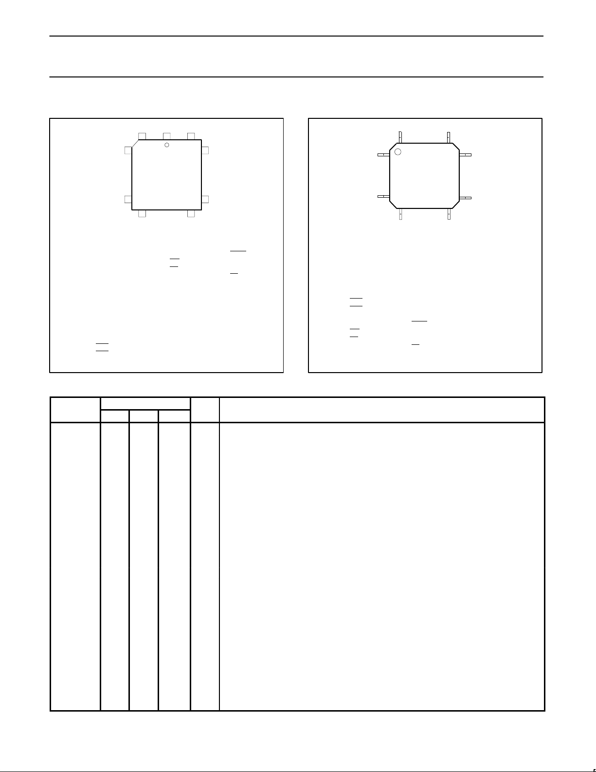
CERAMIC AND PLASTIC LEADED CHIP CARRIER
PIN FUNCTIONS
6140
Pin Function
1 NC*
2 T2/P1.0
3 T2EX/P1.1
4 P1.2
5 P1.3
6 P1.4
7 P1.5
8 P1.6
9 P1.7
10 RST
11 RxD/P3.0
12 NC*
13 TxD/P3.1
14 INT0
15 INT1
* DO NOT CONNECT
/P3.2
/P3.3
7
17
18 28
Pin Function
16 T0/P3.4
17 T1/P3.5
18 WR
19 RD
20 XTAL2
21 XTAL1
22 V
23 NC*
24 P2.0/A8
25 P2.1/A9
26 P2.2/A10
27 P2.3/A11
28 P2.4/A12
29 P2.5/A13
30 P2.6/A14
LCC
SS
/P3.6
/P3.7
39
29
Pin Function
31 P2.7/A15
32 PSEN
33 ALE/PROG
34 NC*
35 EA
/V
36 P0.7/AD7
37 P0.6/AD6
38 P0.5/AD5
39 P0.4/AD4
40 P0.3/AD3
41 P0.2/AD2
42 P0.1/AD1
43 P0.0/AD0
44 V
PP
CC
SU00061
PLASTIC QUAD FLAT PACK
PIN FUNCTIONS
44 34
1
PQFP
11
12 22
Pin Function
1 P1.5
2 P1.6
3 P1.7
4 RST
5 RxD/P3.0
6 NC*
7 TxD/P3.1
8 INT0
/P3.2
9 INT1
10 T0/P3.4
11 T1/P3.5
12 WR
13 RD
14 XTAL2
15 XTAL1
* DO NOT CONNECT
/P3.3
/P3.6
/P3.7
Pin Function
16 V
SS
17 NC*
18 P2.0/A8
19 P2.1/A9
20 P2.2/A10
21 P2.3/A11
22 P2.4/A12
23 P2.5/A13
24 P2.6/A14
25 P2.7/A15
26 PSEN
27 ALE/PROG
28 NC*
29 EA
/V
30 P0.7/AD7
PP
33
23
Pin Function
31 P0.6/AD6
32 P0.5/AD5
33 P0.4/AD4
34 P0.3/AD3
35 P0.2/AD2
36 P0.1/AD1
37 P0.0/AD0
38 V
CC
39 NC*
40 T2/P1.0
41 T2EX/P1.1
42 P1.2
43 P1.3
44 P1.4
SU00062
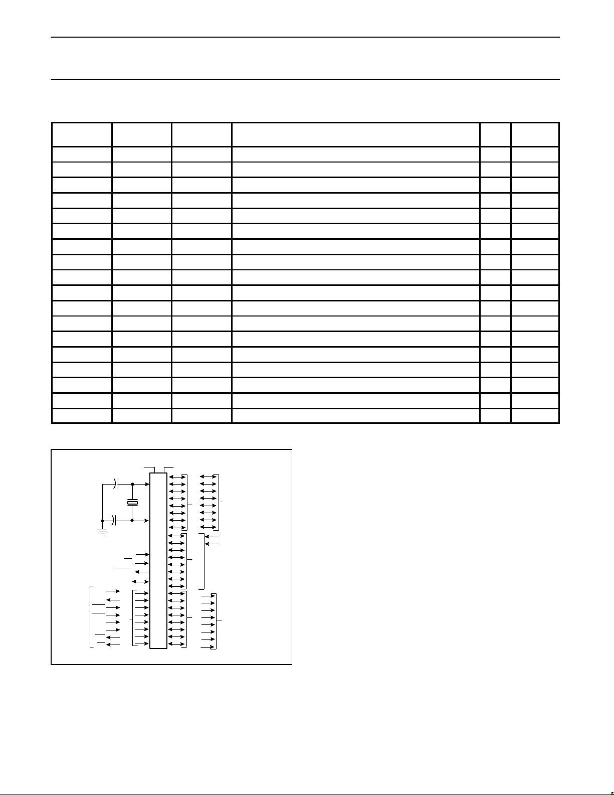
LOGIC SYMBOL
EA
PSEN
ALE/PROG
RxD
TxD
INT0
INT1
T0
T1
WR
RD
SECONDARY FUNCTIONS
XTAL1
XTAL2
RST
/V
PP
V
V
SS
CC
ADDRESS AND
PORT 0
PORT 3
DATA BUS
T2
T2EX
PORT 1PORT 2
ADDRESS BUS
SU00063
1996 Aug 16
4
Page 5

Philips Semiconductors Product specification
80C32/87C52CMOS single-chip 8-bit microcontrollers
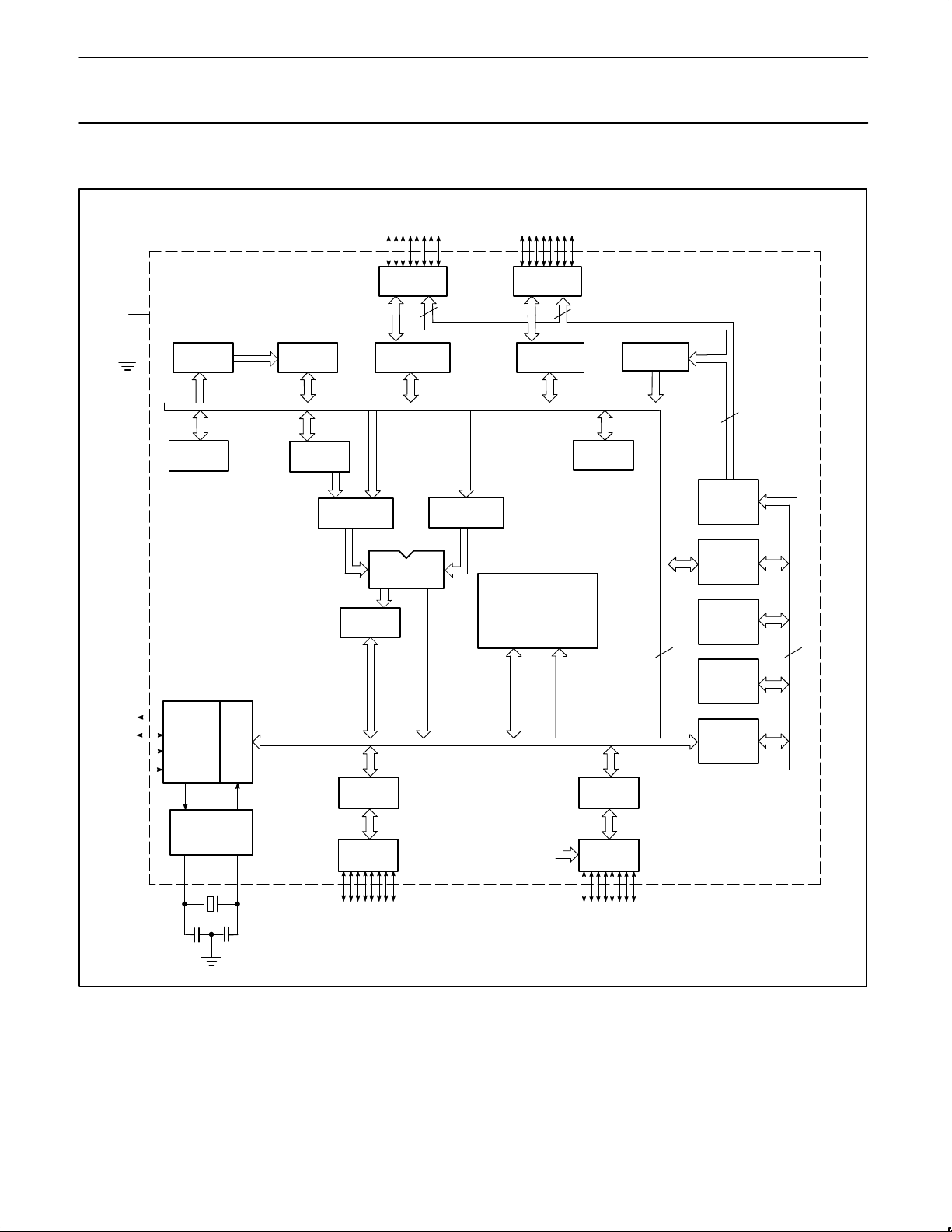
BLOCK DIAGRAM
P0.0–P0.7 P2.0–P2.7
PSEN
ALE
EA
RST
PORT 0
DRIVERS
V
CC
V
SS
PSW
PORT 1
LATCH
PORT 0
LATCH
ALU
TMP1
RAM ADDR
REGISTER
B
REGISTER
TIMING
AND
CONTROL
INSTRUCTION
PD
RAM
ACC
TMP2
REGISTER
PORT 2
DRIVERS
PORT 2
LATCH
STACK
POINTER
PCON SCON TMOD TCON
T2CON TH0 TL0 TH1
TL1 TH2 TL2 RCAP2H
RCAP2L SBUF IE IP
INTERRUPT, SERIAL
PORT AND TIMER BLOCKS
PORT 3
LATCH
ROM/
EPROM
PROGRAM
ADDRESS
REGISTER
BUFFER
PC
INCRE-
MENTER
PROGRAM
COUNTER
DPTR
OSCILLATOR
XTAL1 XTAL2
1996 Aug 16
PORT 1
DRIVERS
P1.0–P1.7
PORT 3
DRIVERS
P3.0–P3.7
SU00064
5
Page 6

Philips Semiconductors Product specification
80C32/87C52CMOS single-chip 8-bit microcontrollers
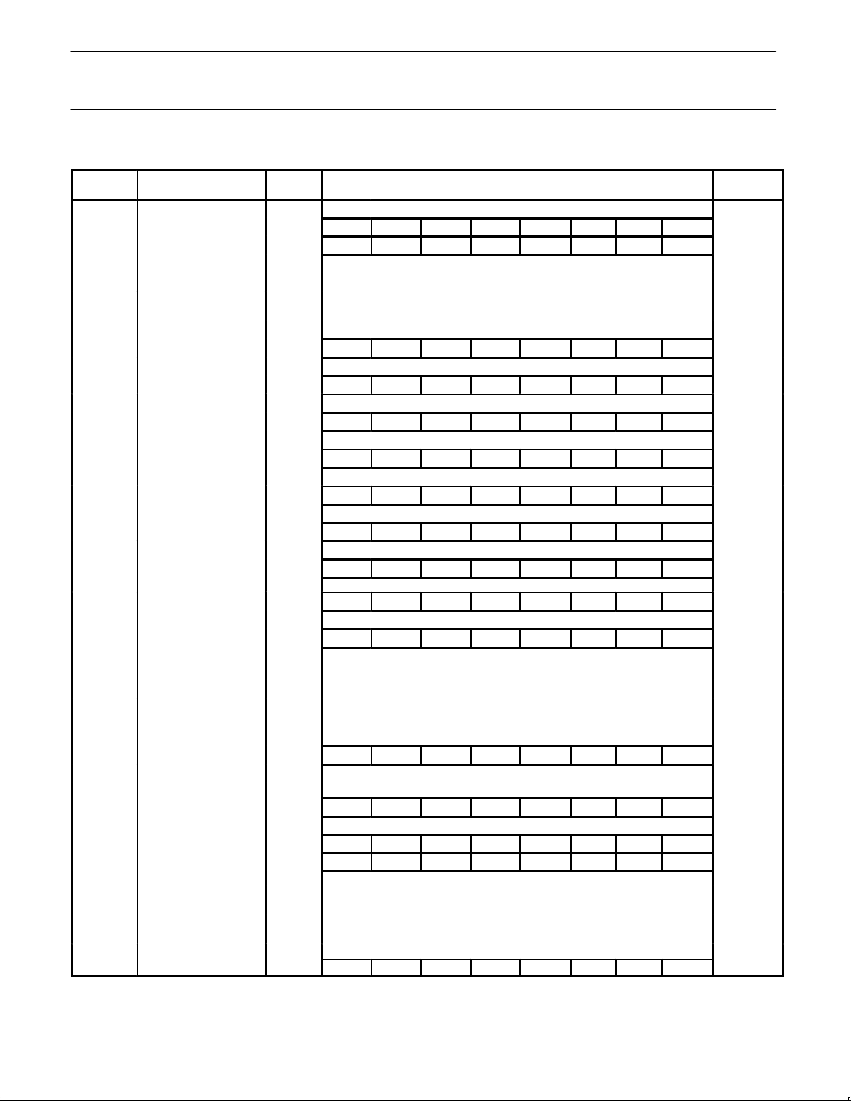
Table 1. 8XC52 Special Function Registers
SYMBOL DESCRIPTION
ACC* Accumulator E0H E7 E6 E5 E4 E3 E2 E1 E0 00H
B* B register F0H F7 F6 F5 F4 F3 F2 F1 F0 00H
DPTR:
DPH
DPL
IE* Interrupt enable A8H EA – ET2 ES ET1 EX1 ET0 EX0 0x000000B
IP* Interrupt priority B8H – – PT2 PS PT1 PX1 PT0 PX0 xx000000B
P0* Port 0 80H AD7 AD6 AD5 AD4 AD3 AD2 AD1 AD0 FFH
Data pointer (2 bytes)
Data pointer high
Data pointer low
DIRECT
ADDRESS
83H
82H
BIT ADDRESS, SYMBOL, OR ALTERNATIVE PORT FUNCTION
MSB LSB
AF AE AD AC AB AA A9 A8
BF BE BD BC BB BA B9 B8
87 86 85 84 83 82 81 80
RESET
VALUE
00H
00H
97 96 95 94 93 92 91 90
P1* Port 1 90H – – – – – – T2EX T2 FFH
A7 A6 A5 A4 A3 A2 A1 A0
P2* Port 2 A0H A15 A14 A13 A12 A11 A10 A9 A8 FFH
B7 B6 B5 B4 B3 B2 B1 B0
P3* Port 3 B0H RD WR T1 T0 INT1 INT0 TxD RxD FFH
1
PCON
PSW* Program status word D0H CY AC F0 RS1 RS0 OV – P 00H
RCAP2H#
RCAPL#
SBUF Serial data buffer 99H xxxxxxxxB
SCON* Serial controller 98H SM0 SM1 SM2 REN TB8 RB8 TI RI 00H
SP Stack pointer 81H 07H
TCON* Timer control 88H TF1 TR1 TF0 TR0 IE1 IT1 IE0 IT0 00H
Power control 87H SMOD – – – GF1 GF0 PD IDL 0xxxxxxxB
D7 D6 D5 D4 D3 D2 D1 D0
Capture high
Capture low
CBH
CAH
00H
00H
9F 9E 9D 9C 9B 9A 99 98
8F 8E 8D 8C 8B 8A 89 88
T2CON*# Timer 2 control C8H TF2 EXF2 RCLK TCLK EXEN2 TR2 C/T2 CP/RL2 00H
TH0
TH1
TH2#
TL0
TL1
TL2#
TMOD Timer mode 89H GATE C/T M1 M0 GATE C/T M1 M0 00H
* Bit addressable
# SFRs are modified from or added to the 80C51 SFRs.
1. Bits GF1, GF0, PD, and IDL of the PCON register are not implemented in the NMOS 8XC52.
1996 Aug 16
Timer high 0
Timer high 1
Timer high 2
Timer low 0
Timer low 1
Timer low 2
8CH
8DH
CDH
8AH
8BH
CCH
CF CE CD CC CB CA C9 C8
00H
00H
00H
00H
00H
00H
6
Page 7
Philips Semiconductors Product specification
80C32/87C52CMOS single-chip 8-bit microcontrollers
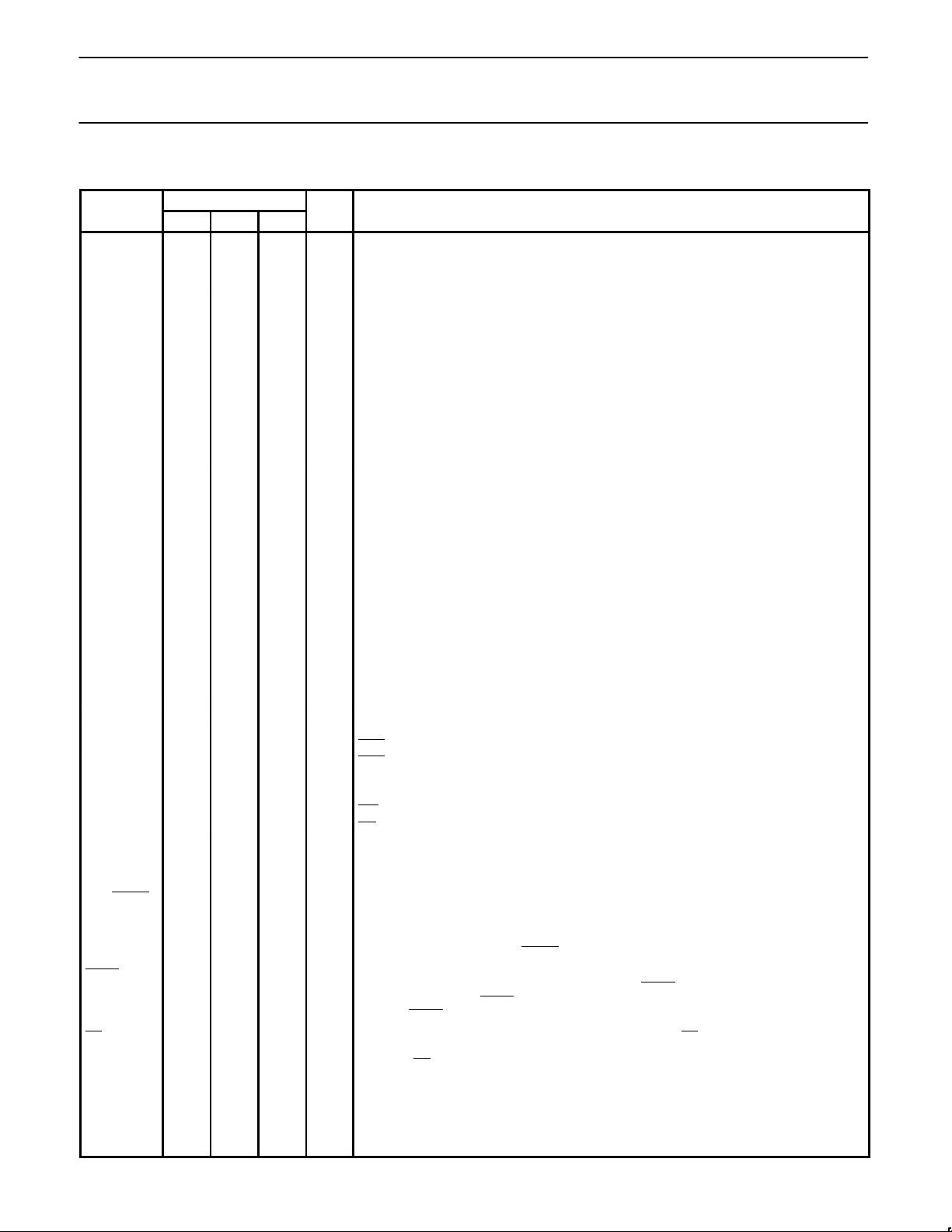
PIN DESCRIPTION
PIN NO.
MNEMONIC DIP LCC QFP TYPE NAME AND FUNCTION
V
SS
V
CC
P0.0–0.7 39–32 43–36 37–30 I/O Port 0: Port 0 is an open-drain, bidirectional I/O port. Port 0 pins that have 1s written to
P1.0–P1.7 1–8 2–9 40–44
P2.0–P2.7 21–28 24–31 18–25 I/O Port 2: Port 2 is an 8-bit bidirectional I/O port with internal pull-ups. Port 2 pins that have 1s
P3.0–P3.7 10–17 11,
RST 9 10 4 I Reset: A high on this pin for two machine cycles while the oscillator is running, resets the
ALE/PROG 30 33 27 I/O Address Latch Enable/Program Pulse: Output pulse for latching the low byte of the
PSEN 29 32 26 O Program Store Enable: The read strobe to external program memory. When the device is
EA/V
PP
XTAL1 19 21 15 I Crystal 1: Input to the inverting oscillator amplifier and input to the internal clock generator
XTAL2 18 20 14 O Crystal 2: Output from the inverting oscillator amplifier.
20 22 16 I Ground: 0V reference.
40 44 38 I Power Supply: This is the power supply voltage for normal, idle, and power-down
operation.
them float and can be used as high-impedance inputs. Port 0 is also the multiplexed
low-order address and data bus during accesses to external program and data memory. In
this application, it uses strong internal pull-ups when emitting 1s. Port 0 also outputs the
code bytes during program verification in the 87C52. External pull-ups are required during
program verification.
I/O Port 1: Port 1 is an 8-bit bidirectional I/O port with internal pull-ups. Port 1 pins that have 1s
1–3
written to them are pulled high by the internal pull-ups and can be used as inputs. As
inputs, port 1 pins that are externally pulled low will source current because of the internal
pull-ups. (See DC Electrical Characteristics: I
receives the low-order address byte during program memory verification. Port 1 also serves
). Pins P1.0 and P1.1 also. Port 1 also
IL
alternate functions for timer 2:
1 2 40 I T2 (P1.0): Timer/counter 2 external count input.
2 3 41 I T2EX (P1.1): Timer/counter 2 trigger input.
written to them are pulled high by the internal pull-ups and can be used as inputs. As
inputs, port 2 pins that are externally being pulled low will source current because of the
internal pull-ups. (See DC Electrical Characteristics: I
address byte during fetches from external program memory and during accesses to
). Port 2 emits the high-order
IL
external data memory that use 16-bit addresses (MOVX @DPTR). In this application, it
uses strong internal pull-ups when emitting 1s. During accesses to external data memory
that use 8-bit addresses (MOV @Ri), port 2 emits the contents of the P2 special function
register.
I/O Port 3: Port 3 is an 8-bit bidirectional I/O port with internal pull-ups. Port 3 pins that have 1s
13–195,7–13
written to them are pulled high by the internal pull-ups and can be used as inputs. As
inputs, port 3 pins that are externally being pulled low will source current because of the
pull-ups. (See DC Electrical Characteristics: I
the 80C51 family , as listed below:
). Port 3 also serves the special features of
IL
10 11 5 I RxD (P3.0): Serial input port
11 13 7 O TxD (P3.1): Serial output port
12 14 8 I INT0 (P3.2): External interrupt
13 15 9 I INT1 (P3.3): External interrupt
14 16 10 I T0 (P3.4): Timer 0 external input
15 17 11 I T1 (P3.5): Timer 1 external input
16 18 12 O WR (P3.6): External data memory write strobe
17 19 13 O RD (P3.7): External data memory read strobe
device. An internal diffused resistor to V
capacitor to V
CC
.
permits a power-on reset using only an external
SS
address during an access to external memory. In normal operation, ALE is emitted at a
constant rate of 1/6 the oscillator frequency, and can be used for external timing or clocking.
Note that one ALE pulse is skipped during each access to external data memory. This pin is
also the program pulse input (PROG
executing code from the external program memory, PSEN
cycle, except that two PSEN
memory. PSEN
is not activated during fetches from internal program memory.
) during EPROM programming.
is activated twice each machine
activations are skipped during each access to external data
31 35 29 I External Access Enable/Programming Supply Voltage: EA must be externally held low
to enable the device to fetch code from external program memory locations 0000H to
1FFFH. If EA
is held high, the device executes from internal program memory unless the
program counter contains an address greater than 1FFFH. This pin also receives the
12.75V programming supply voltage (V
) during EPROM programming.
PP
circuits.
1996 Aug 16
7
Page 8

Philips Semiconductors Product specification
80C32/87C52CMOS single-chip 8-bit microcontrollers
DIFFERENCES FROM THE 80C51
Special Function Registers
The special function register space is the same as the 80C51 except
that the 80C32/87C52 contains the additional special function
registers T2CON, RCAP2L, RCAP2H, TL2, and TH2. Since the
standard 80C51 on-chip functions are identical in the 8XC52, the
SFR locations, bit locations, and operation are likewise identical.
The only exceptions are in the interrupt mode and interrupt priority
SFRs (see Table 1).
Timer/Counters
In addition to timer/counters 0 and 1 of the 80C51, the 80C32/87C52
contains timer/counter 2. Like timers 0 and 1, timer 2 can operate as
either an event timer or as an event counter. This is selected by bit
C/T2 in the special function register T2CON (see Figure 1). It has
three operating modes: capture, auto-load, and baud rate generator,
which are selected by bits in the T2CON as shown in Table 2.
In the Capture Mode there are two options which are selected by bit
EXEN2 in T2CON. If EXEN2 = 0, then Timer 2 is a 16-bit timer or
counter which upon overflowing sets bit TF2, the Timer 2 overflow
bit, which can be used to generate an interrupt. If EXEN2 = 1, then
Timer 2 still does the above, but with the added feature that a 1-to-0
transition at external input T2EX causes the current value in the
Timer 2 registers, TL2 and TH2, to be captured into registers
RCAP2L and RCAP2H, respectively. (RCAP2L and RCAP2H are
new special function registers in the 80C52.) In addition, the
transition at T2EX causes bit EXF2 in T2CON to be set, and EXF2
like TF2 can generate an interrupt. The Capture Mode is illustrated
in Figure 2.
In the auto-reload mode, there are again two options, which are
selected by bit EXEN2 in T2CON. If EXEN2 = 0, then when Timer 2
rolls over it not only sets TF2 but also causes the Timer 2 registers
to be reloaded with the 16-bit value in registers RCAP2L and
RCAP2H, which are preset by software. If EXEN2 = 1, then Timer 2
still does the above, but with the added feature that a 1-to-0
transition at external input T2EX will also trigger the 16-bit reload
and set EXF2. The auto-reload mode is illustrated in Figure 3.
The baud rate generation mode is selected by RCLK = 1 and/or
TCLK = 1. It will be described in conjunction with the serial port.
Serial Port
The serial port of the 8XC52 is identical to that of the 80C51 except
that counter/timer 2 can be used to generate baud rates.
In the 8XC52, Timer 2 is selected as the baud rate generator by
setting TCLK and/or RCLK in T2CON (see Figure 1). Note that the
baud rate for transmit and receive can be simultaneously different.
Setting RCLK and/or TCLK puts Timer into its baud rate generator
mode, as shown in Figure 4.
The baud rate generator mode is similar to the auto-reload mode, in
that a rollover in TH2 causes the Timer 2 registers to be reloaded
with the 16-bit value in registers RCAP2H and RCAP2L, which are
preset by software.
Now, the baud rates in Modes 1 and 3 are determined by T imer 2’s
overflow rate as follows:
Modes 1, 3 Baud Rate
The timer can be configured for either “timer” or “counter” operation.
In the most typical applications, it is configured for “timer” operation
(C/T2 = 0). “Timer” operation is a little different for Timer 2 when it’s
being used as a baud rate generator. Normally, as a timer it would
increment every machine cycle (thus at 1/12 the oscillator
frequency). As a baud rate generator, however, it increments every
state time (thus at 1/2 the oscillator frequency). In that case the
baud rate is given by the formula:
Modes 1, 3 Baud Rate
where (RCAP2H, RCAP2L) is the content of RCAP2H and RCAP2L
taken as a 16-bit unsigned integer.
Timer 2 Overflow Rate
16
Oscillator Frequency
32 [65536 (RCAP2H, RCAP2L)]
Symbol Position Name and Significance
TF2 T2CON.7 Timer 2 overflow flag set by a Timer 2 overflow and must be cleared by software. TF2 will not be set when either RCLK or TCLK = 1.
EXF2 T2CON.6 Timer 2 external flag set when either a capture or reload is caused by a negative transition on T2EX and EXEN2 = 1. When Timer 2
RCLK T2CON.5 Receive clock flag. When set, causes the serial port to use Timer 2 overflow pulses for its receive clock in modes 1 and 3. RCLK = 0
TCLK T2CON.4 Transmit clock flag. When set, causes the serial port to use Timer 2 overflow pulses for its transmit clock in modes 1 and 3. TCLK = 0
EXEN2 T2CON.3 Timer 2 external enable flag. When set, allows a capture or reload to occur as a result of a negative transition on T2EX if Timer 2 is not
TR2 T2CON.2 Start/stop control for Timer 2. A logic 1 starts the timer.
C/T2 T2CON.1 Timer or counter select. (Timer 2)
CP/RL2
1996 Aug 16
(MSB) (LSB)
EXF2 RCLK TCLK EXEN2 TR2 C/T2 CP/RL2
TF2
interrupt is enabled, EXF2 = 1 will cause the CPU to vector to the Timer 2 interrupt routine. EXF2 must be cleared by software.
causes Timer 1 overflow to be used for the receive clock.
causes Timer 1 overflows to be used for the transmit clock.
being used to clock the serial port. EXEN2 = 0 causes Timer 2 to ignore events at T2EX.
0 = Internal timer (OSC/12)
1 = External event counter (falling edge triggered).
T2CON.0 Capture/Reload flag. When set, captures will occur on negative transitions at T2EX if EXEN2 = 1. When cleared, auto-reloads will
occur either with Timer 2 overflows or negative transitions at T2EX when EXEN2 = 1. When either RCLK = 1 or TCLK = 1, this bit is
ignored and the timer is forced to auto-reload on Timer 2 overflow.
Figure 1. Timer/Counter 2 (T2CON) Control Register
8
SU00065
Page 9

Philips Semiconductors Product specification
80C32/87C52CMOS single-chip 8-bit microcontrollers
T2 Pin
T2EX Pin
T2 PIN
OSC
OSC
÷ 12
Transition
Detector
÷ 12
C/T2 = 0
C/T2
= 1
C/T2 = 0
= 1
C/T2
EXEN2
Control
TR2
Capture
RCAP2L RCAP2H
Control
Figure 2. Timer 2 in Capture Mode
CONTROL
TL2
(8-bits)
TL2
(8-BITS)
TH2
(8-bits)
TH2
(8-BITS)
TF2
EXF2
Timer 2
Interrupt
SU00066
T2EX PIN
TRANSITION
DETECTOR
EXEN2
TR2
RELOAD
RCAP2L RCAP2H
CONTROL
Figure 3. Timer 2 in Auto-Reload Mode
TF2
EXF2
TIMER 2
INTERRUPT
SU00067
1996 Aug 16
9
Page 10

Philips Semiconductors Product specification
80C32/87C52CMOS single-chip 8-bit microcontrollers
Timer 1
Overflow
NOTE: OSC. Freq. is divided by 2, not 12.
OSC
T2 Pin
T2EX Pin
÷ 2
Transition
Detector
C/T2 = 0
C/T2
= 1
EXEN2
Note availability of additional external interrupt.
Control
TR2
Control
EXF2
TL2
(8-bits)
RCAP2L RCAP2H
Timer 2
Interrupt
TH2
(8-bits)
Reload
Figure 4. Timer 2 in Baud Rate Generator Mode
Table 2. Timer 2 Operating Modes
RCLK + TCLK CP/RL2 TR2 MODE
0 0 1 16-bit Auto-reload
0 1 1 16-bit Capture
1 X 1 Baud rate generator
X X 0 (off)
÷ 2
“0” “1”
“0”“1”
SMOD
RCLK
÷ 16
“0”“1”
÷ 16 TX Clock
RX Clock
TCLK
SU00068
Timer 2 as a baud rate generator is shown in Figure 4. This figure is
valid only if RCLK + TCLK = 1 in T2CON. Note that a rollover in TH2
does not set TF2, and will not generate an interrupt. Therefore, the
Timer 2 interrupt does not have to be disabled when Timer 2 is in
the baud rate generator mode. Note too, that if EXEN2 is set, a
1-to-0 transition in T2EX will set EXF2 but will not cause a reload
from (RCAP2H, RCAP2L) to (TH2, TL2). Thus when Timer 2 is in
use as a baud rate generator, T2EX can be used as an extra
external interrupt, if desired.
It should be noted that when Timer 2 is running (TR2 = 1) in “timer”
function in the baud rate generator mode, one should not try to read
or write TH2 or TL2. Under these conditions the timer is being
incremented every state time, and the results of a read or write may
not be accurate. The RCAP registers may be read, but should not
be written to, because a write might overlap a reload and cause
write and/or reload errors. Turn the timer off (clear TR2) before
accessing the Timer 2 or RCAP registers, in this case.
1996 Aug 16
Timer/Counter 2 Set-up
Except for the baud rate generator mode, the values given for
T2CON do not include the setting of the TR2 bit. Therefore, bit TR2
must be set, separately, to turn the timer on. See Table 3 for set-up
of timer 2 as a timer. See Table 4 for set-up of timer 2 as a counter.
Using Timer/Counter 2 to Generate Baud Rates
For this purpose, Timer 2 must be used in the baud rate generating
mode. If Timer 2 is being clocked through pin T2 (P1.0) the baud
rate is:
Baud Rate
And if it is being clocked internally, the baud rate is:
Baud Rate
To obtain the reload value for RCAP2H and RCA02L, the above
equation can be rewritten as:
RCAP2H,RCAP2L 65536
10
Timer 2 Overflow Rate
16
Oscillator Frequency
32 [65536 (RCAP2H,RCAP2L)]
Oscillator Frequency
32 Baud Rate
Page 11

Philips Semiconductors Product specification
80C32/87C52CMOS single-chip 8-bit microcontrollers
Interrupts
The 80C32/87C52 has 6 interrupt sources. All except TF2 and EXF2
are identical sources to those in the 80C51.
The Interrupt Enable Register and the Interrupt Priority Register are
modified to include the additional 80C32/87C52 interrupt sources.
The operation of these registers is identical to the 80C51.
In the 80C32/87C52, the Timer 2 Interrupt is generated by the
logical OR of TF2 and EXF2. Neither of these flags is cleared by
hardware when the service routine is vectored to. In fact, the service
routine may have to determine whether it was TF2 or EXF2 that
generated the interrupt, and the bit will have to be cleared in
software.
All of the bits that generate interrupts can be set or cleared by
software, with the same result as though it has been set or cleared
by hardware. That is, interrupts can be generated or pending
interrupts can be canceled in software.
The interrupt vector addresses and the interrupt priority for requests
in the same priority level are given in the following:
Source Vector Priority Within
Address Level
1. IE0 0003H (highest)
2. TF0 000BH
3. IE1 0013H
4. TF1 001BH
5. RI + TI 0023H
6. TF2 + EXF2 002BH (lowest)
Note that they are identical to those in the 80C51 except for the
addition of the Timer 2 (TF1 and EXF2) interrupt at 002BH and at
the lowest priority within a level.
Table 3. Timer 2 as a Timer
MODE T2CON
INTERNAL CONTROL
(Note 1)
16-bit Auto-Reload 00H 08H
16-bit Capture 01H 09H
Baud rate generator receive and transmit same baud rate 34H 36H
Receive only 24H 26H
Transmit only 14H 16H
EXTERNAL CONTROL
(Note 2)
Table 4. Timer 2 as a Counter
MODE TMOD
INTERNAL CONTROL
(Note 1)
16-bit 02H 0AH
Auto-Reload 03H 0BH
NOTES:
1. Capture/reload occurs only on timer/counter overflow.
2. Capture/reload occurs on timer/counter overflow and a 1-to-0 transition on T2EX (P1.1) pin except when timer 2 is used in the baud rate
generator mode.
EXTERNAL CONTROL
(Note 2)
1996 Aug 16
11
Page 12

Philips Semiconductors Product specification
80C32/87C52CMOS single-chip 8-bit microcontrollers
OSCILLA T OR CHARACTERISTICS
XTAL1 and XTAL2 are the input and output, respectively , of an
inverting amplifier . The pins can be configured for use as an on-chip
oscillator, as shown in the Logic Symbol, page 4.
To drive the device from an external clock source, XTAL1 should be
driven while XTAL2 is left unconnected. There are no requirements
on the duty cycle of the external clock signal, because the input to
the internal clock circuitry is through a divide-by-two flip-flop.
However, minimum and maximum high and low times specified in
the data sheet must be observed.
RESET
A reset is accomplished by holding the RST pin high for at least two
machine cycles (24 oscillator periods), while the oscillator is running.
To insure a good power-up reset, the RST pin must be high long
enough to allow the oscillator time to start up (normally a few
milliseconds) plus two machine cycles.
IDLE MODE
In idle mode, the CPU puts itself to sleep while all of the on-chip
peripherals stay active. The instruction to invoke the idle mode is the
last instruction executed in the normal operating mode before the
idle mode is activated. The CPU contents, the on-chip RAM, and all
of the special function registers remain intact during this mode. The
idle mode can be terminated either by any enabled interrupt (at
which time the process is picked up at the interrupt service routine
and continued), or by a hardware reset which starts the processor in
the same manner as a power-on reset.
POWER-DOWN MODE
In the power-down mode, the oscillator is stopped and the
instruction to invoke power-down is the last instruction executed.
Only the contents of the on-chip RAM are preserved. A hardware
reset is the only way to terminate the power-down mode. the control
bits for the reduced power modes are in the special function register
PCON.
DESIGN CONSIDERATIONS
At power-on, the voltage on VCC and RST must come up at the
same time for a proper start-up.
Table 5 shows the state of I/O ports during low current operating
modes.
As a precaution to coming out of an unexpected power down, INT0
and INT1 should be disabled prior to enterring power down.
Table 5. External Pin Status During Idle and Power-Down Modes
MODE PROGRAM MEMORY ALE PSEN PORT 0 PORT 1 PORT 2 PORT 3
Idle Internal 1 1 Data Data Data Data
Idle External 1 1 Float Data Address Data
Power-down Internal 0 0 Data Data Data Data
Power-down External 0 0 Float Data Data Data
1996 Aug 16
12
Page 13

Philips Semiconductors Product specification
80C32/87C52CMOS single-chip 8-bit microcontrollers
Electrical Deviations from Commercial Specifications for Extended Temperature Range (87C52)
DC and AC parameters not included here are the same as in the commercial temperature range table.
DC ELECTRICAL CHARACTERISTICS
T
= –40°C to +85°C, VCC = 5V ±10%, VSS = 0V
amb
TEST LIMITS
SYMBOL PARAMETER CONDITIONS MIN MAX UNIT
V
IL
V
IL1
V
IH
V
IH1
I
IL
I
TL
I
CC
Input low voltage, except EA –0.5 0.2VCC–0.15 V
Input low voltage to EA 0 0.2VCC–0.35 V
Input high voltage, except XTAL1, RST 0.2VCC+1 VCC+0.5 V
Input high voltage to XTAL1, RST 0.7VCC+0.1 VCC+0.5 V
Logical 0 input current, ports 1, 2, 3 VIN = 0.45V –75 µA
Logical 1-to-0 transition current, ports 1, 2, 3 VIN = 2.0V –750 µA
Power supply current:
Active mode
Idle mode
Power-down mode
VCC = 4.5–5.5V ,
Frequency range =
3.5 to 16MHz
32
50
5
mA
µA
mA
ABSOLUTE MAXIMUM RATINGS
1, 2, 3
PARAMETER RATING UNIT
Operating temperature under bias 0 to +70 or –40 to +85 °C
Storage temperature range –65 to +150 °C
Voltage on EA/VPP pin to V
Voltage on any other pin to V
SS
SS
0 to +13.0 V
–0.5 to +6.5 V
Maximum IOL per I/O pin 15 mA
Power dissipation (based on package heat transfer limitations, not
1.5 W
device power consumption)
NOTES:
1. Stresses above those listed under Absolute Maximum Ratings may cause permanent damage to the device. This is a stress rating only and
functional operation of the device at these or any conditions other than those described in the AC and DC Electrical Characteristics section
of this specification is not implied.
2. This product includes circuitry specifically designed for the protection of its internal devices from the damaging effects of excessive static
charge. Nonetheless, it is suggested that conventional precautions be taken to avoid applying greater than the rated maxima.
3. Parameters are valid over operating temperature range unless otherwise specified. All voltages are with respect to V
noted.
unless otherwise
SS
1996 Aug 16
13
Page 14
Philips Semiconductors Product specification
80C32/87C52CMOS single-chip 8-bit microcontrollers
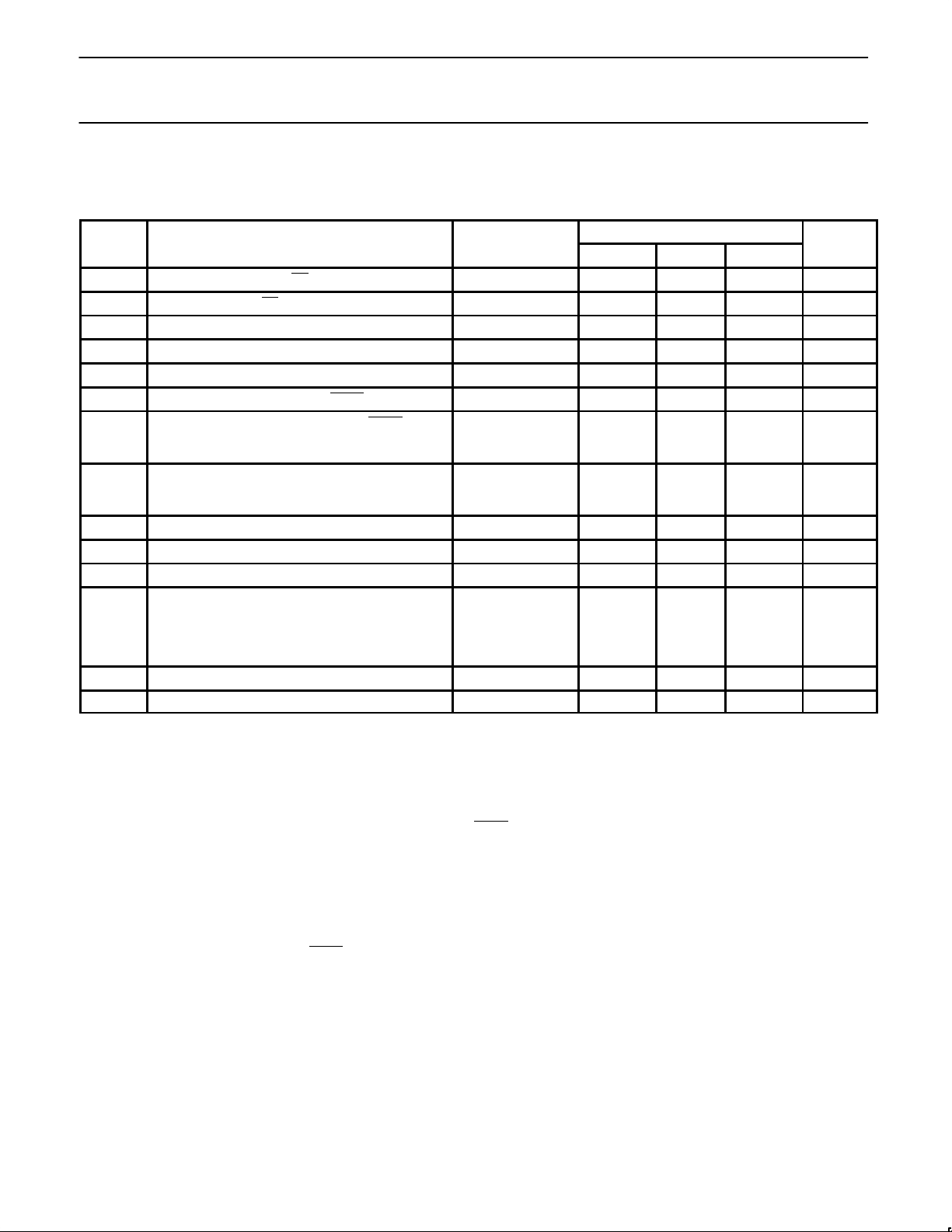
DC ELECTRICAL CHARACTERISTICS
T
= 0°C to +70°C or –40°C to +85°C, VCC = 5V ±10%, VSS = 0V (87C52)
amb
= 0°C to +70°C or –40°C to +85°C, VCC = 5V ±10%, VSS = 0V (80C32)
T
amb
TEST LIMITS
SYMBOL PARAMETER CONDITIONS MIN TYP
V
V
V
V
V
V
V
V
I
I
I
I
IL
TL
LI
CC
IL
IL1
IH
IH1
OL
OL1
OH
OH1
Input low voltage, except EA
Input low voltage to EA
Input high voltage, except XTAL1, RST
Input high voltage, XTAL1, RST
Output low voltage, ports 1, 2, 3
Output low voltage, port 0, ALE, PSEN
Output high voltage, ports 1, 2, 3, ALE, PSEN
Output high voltage (port 0 in external bus mode) IOH = –800µA,
Logical 0 input current, ports 1, 2, 3
Logical 1-to-0 transition current, ports 1, 2, 3
Input leakage current, port 0 VIN = VIL or V
Power supply current:
Active mode @ 16MHz
7
7
7
7
9
9
3
IOL = 1.6mA
IOL = 3.2mA
IOH = –60µA,
I
OH
I
OH
2
2
= –25µA
= –10µA
–0.5 0.2VCC–0.1 V
0 0.2VCC–0.3 V
0.2VCC+0.9 VCC+0.5 V
0.7V
CC
2.4
0.75V
CC
0.9V
CC
2.4
= –300µA
I
OH
= –80µA
I
OH
7
7
7
5
VIN = 0.45V –50 µA
See note 4 –650 µA
See note 6
0.75V
CC
0.9V
CC
IH
Idle mode @ 16MHz
Power-down mode T
R
RST
C
IO
Internal reset pull-down resistor 50 300 kΩ
Pin capacitance
10
= 0 to 70°C
amb
= –40 to +85°C
T
amb
NOTES:
1. Typical ratings are not guaranteed. The values listed are at room temperature, 5V.
2. Capacitive loading on ports 0 and 2 may cause spurious noise to be superimposed on the V
to external bus capacitance discharging into the port 0 and port 2 pins when these pins make 1-to-0 transitions during bus operations. In the
s of ALE and ports 1 and 3. The noise is due
OL
worst cases (capacitive loading > 100pF), the noise pulse on the ALE pin may exceed 0.8V . In such cases, it may be desirable to qualify
ALE with a Schmitt Trigger, or use an address latch with a Schmitt Trigger STROBE input. I
single output sinks more than 5mA and no more than two outputs exceed the test conditions.
3. Capacitive loading on ports 0 and 2 may cause the V
address bits are stabilizing.
on ALE and PSEN to momentarily fall below the 0.9VCC specification when the
OH
can exceed these conditions provided that no
OL
4. Pins of ports 1, 2 and 3 source a transition current when they are being externally driven from 1 to 0. The transition current reaches its
maximum value when V
5. I
at other frequencies is given by: Active mode: I
CCMAX
where FREQ is the external oscillator frequency in MHz. I
6. See Figures 13 through 16 for I
7. These values apply only to T
8. Load capacitance for port 0, ALE, and PSEN
9. Under steady state (non-transient) conditions, I
exceeds the test condition, VOL may exceed the related specification. Pins are not guaranteed to sink current greater than the listed
If I
OL
test conditions.
is approximately 2V .
IN
test conditions.
CC
= 0°C to +70°C. For T
amb
Maximum I
Maximum I
Maximum total I
per port pin: 15mA (*NOTE: This is 85°C specification.)
OL
per 8-bit port: 26mA
OL
= 1.5 × FREQ + 8.0: Idle mode: I
CCMAX
amb
is given in mA. See Figure 12.
CCMAX
= –40°C to +85°C, see table on previous page.
= 100pF, load capacitance for all other outputs = 80pF .
must be externally limited as follows:
OL
for all outputs: 67mA
OL
CCMAX
10.This limit is for plastic packages. For ceramic packages, the maximum limit is 20pF.
1
MAX UNIT
VCC+0.5 V
0.45 V
0.45 V
±10 µA
11.5
1.3
3
32
5
50
75
15 pF
= 0.14 × FREQ +2.31,
V
V
V
V
V
V
mA
mA
µA
µA
1996 Aug 16
14
Page 15
Philips Semiconductors Product specification
80C32/87C52CMOS single-chip 8-bit microcontrollers
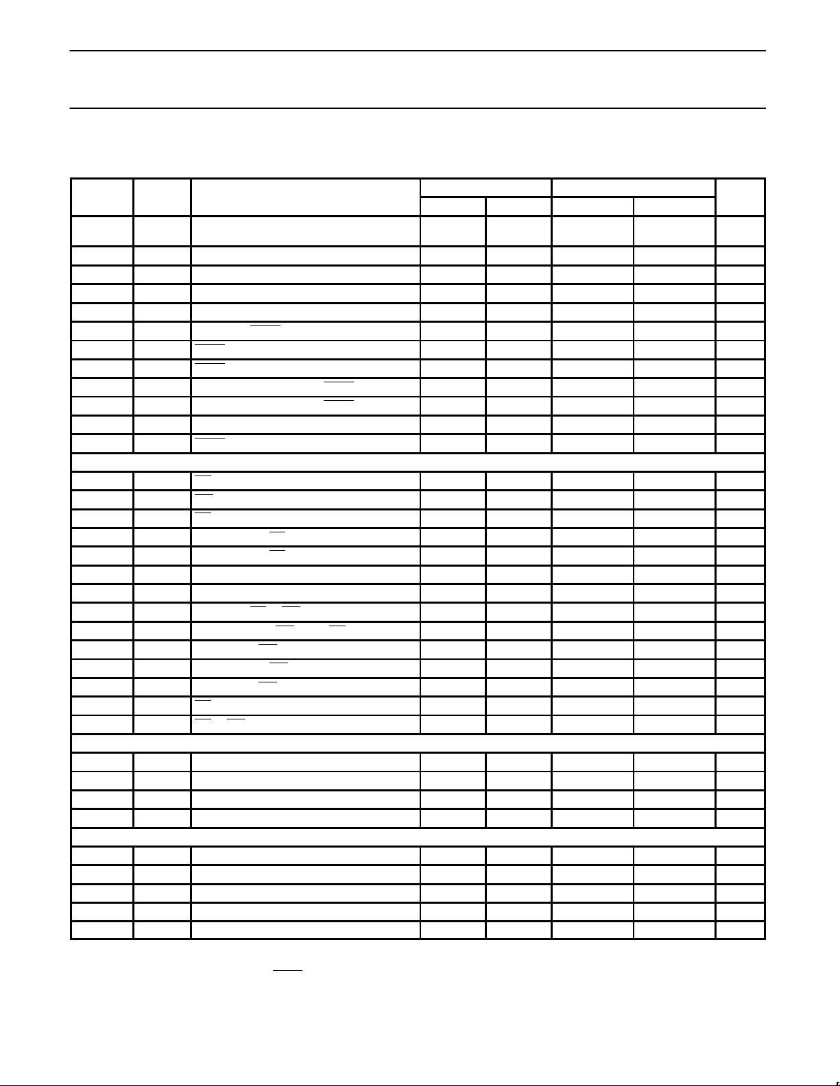
AC ELECTRICAL CHARACTERISTICS
T
= 0°C to +70°C or –40°C to +85°C, VCC = 5V ±10%, VSS = 0V (87C52)
amb
1, 2, 3
16MHz CLOCK VARIABLE CLOCK
SYMBOL FIGURE PARAMETER MIN MAX MIN MAX UNIT
1/t
t
LHLL
t
AVLL
t
LLAX
t
LLIV
t
LLPL
t
PLPH
t
PLIV
t
PXIX
t
PXIZ
t
AVIV
t
PLAZ
CLCL
5 Oscillator frequency
Speed versions : E
5 ALE pulse width 85 2t
5 Address valid to ALE low 22 t
5 Address hold after ALE low 32 t
5 ALE low to valid instruction in 150 4t
5 ALE low to PSEN low 32 t
5 PSEN pulse width 142 3t
5 PSEN low to valid instruction in 82 3t
3.5 16 MHz
–40 ns
CLCL
–40 ns
CLCL
–30 ns
CLCL
–100 ns
CLCL
–30 ns
CLCL
–45 ns
CLCL
–105 ns
CLCL
5 Input instruction hold after PSEN 0 0 ns
5 Input instruction float after PSEN 37 t
5 Address to valid instruction in 207 5t
–25 ns
CLCL
–105 ns
CLCL
5 PSEN low to address float 10 10 ns
Data Memory
t
RLRH
t
WLWH
t
RLDV
t
RHDX
t
RHDZ
t
LLDV
t
AVDV
t
LLWL
t
AVWL
t
QVWX
t
WHQX
t
QVWH
t
RLAZ
t
WHLH
6, 7 RD pulse width 275 6t
6, 7 WR pulse width 275 6t
6, 7 RD low to valid data in 147 5t
–100 ns
CLCL
–100 ns
CLCL
–165 ns
CLCL
6, 7 Data hold after RD 0 0 ns
6, 7 Data float after RD 65 2t
6, 7 ALE low to valid data in 350 8t
6, 7 Address to valid data in 397 9t
6, 7 ALE low to RD or WR low 137 239 3t
6, 7 Address valid to WR low or RD low 122 4t
6, 7 Data valid to WR transition 13 t
6, 7 Data hold after WR 13 t
7 Data valid to WR high 287 7t
–50 3t
CLCL
–130 ns
CLCL
–50 ns
CLCL
–50 ns
CLCL
–150 ns
CLCL
–60 ns
CLCL
–150 ns
CLCL
–165 ns
CLCL
+50 ns
CLCL
6, 7 RD low to address float 0 0 ns
6, 7 RD or WR high to ALE high 23 103 t
–40 t
CLCL
+40 ns
CLCL
External Clock
t
CHCX
t
CLCX
t
CLCH
t
CHCL
9 High time 20 20 t
9 Low time 20 20 t
CLCL–tCLCX
CLCL–tCHCX
9 Rise time 20 20 ns
9 Fall time 20 20 ns
Shift Register
t
XLXL
t
QVXH
t
XHQX
t
XHDX
t
XHDV
8 Serial port clock cycle time 750 12t
8 Output data setup to clock rising edge 492 10t
8 Output data hold after clock rising edge 8 2t
CLCL
–133 ns
CLCL
–117 ns
CLCL
8 Input data hold after clock rising edge 0 0 ns
8 Clock rising edge to input data valid 492 10t
–133 ns
CLCL
NOTES:
1. Parameters are valid over operating temperature range unless otherwise specified.
2. Load capacitance for port 0, ALE, and PSEN
= 100pF, load capacitance for all other outputs = 80pF .
3. Interfacing the 80C32/52 to devices with float times up to 45ns is permitted. This limited bus contention will not cause damage to Port 0
drivers.
4. See application note AN457 for external memory interface.
ns
ns
ns
1996 Aug 16
15
Page 16

Philips Semiconductors Product specification
80C32/87C52CMOS single-chip 8-bit microcontrollers
AC ELECTRICAL CHARACTERISTICS
T
= 0°C to +70°C or –40°C to +85°C, VCC = 5V ±10%, VSS = 0V
amb
1, 2, 3
24MHz CLOCK VARIABLE CLOCK 33MHz CLOCK
SYMBOL FIGURE PARAMETER MIN MAX MIN MAX MIN MAX UNIT
1/t
t
LHLL
t
AVLL
t
LLAX
t
LLIV
t
LLPL
t
PLPH
t
PLIV
t
PXIX
t
PXIZ
t
AVIV
t
PLAZ
CLCL
5 Oscillator frequency
Speed versions : I
3.5 24
:N
5 ALE pulse width 43 2t
5 Address valid to ALE low 17 t
5 Address hold after ALE low 17 t
–40 21 ns
CLCL
–25 5 ns
CLCL
–25 5 ns
CLCL
5 ALE low to valid instruction in 102 4t
5 ALE low to PSEN low 17 t
5 PSEN pulse width 80 3t
–25 5 ns
CLCL
–45 46 ns
CLCL
5 PSEN low to valid instruction in 65 3t
3.5 33
–65 56 ns
CLCL
–60 31 ns
CLCL
MHz
5 Input instruction hold after PSEN 0 0 0 ns
5 Input instruction float after PSEN 17 t
5 Address to valid instruction in 128 5t
–25 5 ns
CLCL
–80 72 ns
CLCL
5 PSEN low to address float 10 10 10 ns
Data Memory
t
RLRH
t
WLWH
t
RLDV
t
RHDX
t
RHDZ
t
LLDV
t
AVDV
t
LLWL
t
AVWL
t
QVWX
t
WHQX
t
QVWH
t
RLAZ
t
WHLH
6, 7 RD pulse width 150 6t
6, 7 WR pulse width 150 6t
6, 7 RD low to valid data in 118 5t
–100 82 ns
CLCL
–100 82 ns
CLCL
–90 62 ns
CLCL
6, 7 Data hold after RD 0 0 0 ns
6, 7 Data float after RD 55 2t
6, 7 ALE low to valid data in 183 8t
6, 7 Address to valid data in 210 9t
6, 7 ALE low to RD or WR low 75 175 3t
6, 7 Address valid to WR low or RD low 92 4t
6, 7 Data valid to WR transition 12 t
6, 7 Data hold after WR 17 t
7 Data valid to WR high 162 7t
–50 3t
CLCL
–75 46 ns
CLCL
–30 0.3 ns
CLCL
–25 5 ns
CLCL
–130 82 ns
CLCL
–28 33 ns
CLCL
–150 92 ns
CLCL
–165 108 ns
CLCL
+50 41 141 ns
CLCL
6, 7 RD low to address float 0 0 0 ns
6, 7 RD or WR high to ALE high 17 67 t
CLCL
–25 t
+25 5 5 ns
CLCL
External Clock
t
CHCX
t
CLCX
t
CLCH
t
CHCL
9 High time 17 17 t
9 Low time 17 17 t
CLCL–tCLCX
CLCL–tCHCX
ns
ns
9 Rise time 5 5 ns
9 Fall time 5 5 ns
Shift Register
t
XLXL
t
QVXH
t
XHQX
t
XHDX
t
XHDV
8 Serial port clock cycle time 505 12t
8 Output data setup to clock rising edge 283 10t
8 Output data hold after clock rising edge 3 2t
CLCL
CLCL
CLCL
–133 170 ns
–80 19 ns
363 ns
8 Input data hold after clock rising edge 0 0 0 ns
8 Clock rising edge to input data valid 283 10t
–133 170 ns
CLCL
NOTES:
1. Parameters are valid over operating temperature range unless otherwise specified.
2. Load capacitance for port 0, ALE, and PSEN
= 100pF, load capacitance for all other outputs = 80pF .
3. Interfacing the 8XC52 to devices with float times up to 45ns is permitted. This limited bus contention will not cause damage to Port 0 drivers.
4. Variable clock is specified for oscillator frequencies greater than 16MHz to 33MHz. For frequencies equal or less than 16MHz, see 16MHz
“AC Electrial Characteristics”, page 15.
1996 Aug 16
16
Page 17

Philips Semiconductors Product specification
80C32/87C52CMOS single-chip 8-bit microcontrollers
EXPLANATION OF THE AC SYMBOLS
Each timing symbol has five characters. The first character is always
‘t’ (= time). The other characters, depending on their positions,
indicate the name of a signal or the logical status of that signal. The
designations are:
A – Address
C – Clock
D – Input data
H – Logic level high
I – Instruction (program memory contents)
L – Logic level low, or ALE
t
ALE
LHLL
P – PSEN
Q – Output data
R–RD
signal
t – Time
V – Valid
W– WR
signal
X – No longer a valid logic level
Z – Float
Examples: t
= Time for address valid to ALE low.
AVLL
t
= Time for ALE low to PSEN low.
LLPL
ALE
PSEN
RD
PSEN
PORT 0
PORT 2
t
t
AVLL
LLPL
t
LLAX
A0–A7 A0–A7
t
AVIV
t
PLPH
t
LLIV
t
PLIV
t
t
PLAZ
t
PXIX
INSTR IN
A0–A15 A8–A15
PXIZ
Figure 5. External Program Memory Read Cycle
t
WHLH
t
LLDV
t
LLWL
t
RLRH
SU00006
t
AVLL
PORT 0
PORT 2
1996 Aug 16
t
LLAX
A0–A7
FROM RI OR DPL
t
AVWL
t
t
t
RLAZ
t
AVDV
P2.0–P2.7 OR A8–A15 FROM DPF A0–A15 FROM PCH
RLDV
t
RHDX
DATA IN A0–A7 FROM PCL INSTR IN
RHDZ
Figure 6. External Data Memory Read Cycle
17
SU00025
Page 18

Philips Semiconductors Product specification
80C32/87C52CMOS single-chip 8-bit microcontrollers
ALE
t
WHLH
PSEN
WR
PORT 0
PORT 2
INSTRUCTION
ALE
CLOCK
OUTPUT DATA
WRITE TO SBUF
INPUT DATA
CLEAR RI
t
WLWH
t
WHQX
DATA OUT A0–A7 FROM PCL INSTR IN
SU00069
t
AVLL
t
t
LLAX
A0–A7
FROM RI OR DPL
t
AVWL
LLWL
t
QVWX
P2.0–P2.7 OR A8–A15 FROM DPF A0–A15 FROM PCH
Figure 7. External Data Memory Write Cycle
012345678
t
XLXL
t
t
QVXH
t
XHDV
VALID VALID VALID VALID VALID VALID VALID VALID
XHQX
1230 4567
t
XHDX
SET TI
SET RI
SU00027
Figure 8. Shift Register Mode Timing
1996 Aug 16
VCC–0.5
0.45V
0.7V
CC
0.2VCC–0.1
t
CHCL
t
CLCX
t
CLCL
t
CHCX
t
Figure 9. External Clock Drive
18
CLCH
SU00009
Page 19

Philips Semiconductors Product specification
80C32/87C52CMOS single-chip 8-bit microcontrollers
VCC–0.5
0.45V
NOTE:
AC inputs during testing are driven at VCC –0.5 for a logic ‘1’ and 0.45V for a logic ‘0’.
Timing measurements are made at VIH min for a logic ‘1’ and VIL max for a logic ‘0’.
0.2V
0.2V
CC
CC
+0.9
–0.1
Figure 10. AC Testing Input/Output
V
+0.1V
V
LOAD
LOAD
NOTE:
For timing purposes, a port is no longer floating when a 100mV change from load voltage occurs,
and begins to float when a 100mV change from the loaded V
V
LOAD
–0.1V
TIMING
REFERENCE
POINTS
OH/VOL
VOH–0.1V
VOL+0.1V
level occurs. IOH/IOL ≥ ±20mA.
Figure 11. Float Waveform
65
60
55
MAX ACTIVE MODE
ICCMAX = 1.5 X FREQ. + 8.0
SU00010
SU00011
50
45
40
35
I
mA
CC
30
25
20
15
10
5
4MHz 8MHz 12MHz 16MHz
TYP ACTIVE MODE
MAX IDLE MODE
20MHz
FREQ AT XTAL1
TYP IDLE MODE
24MHz 28MHz 32MHz 36MHz
Figure 12. ICC vs. FREQ
Valid only within frequency specifications of the device under test
SU00070B
1996 Aug 16
19
Page 20
Philips Semiconductors Product specification
80C32/87C52CMOS single-chip 8-bit microcontrollers
V
CC
RST
(NC)
CLOCK SIGNAL
XTAL2
XTAL1
V
SS
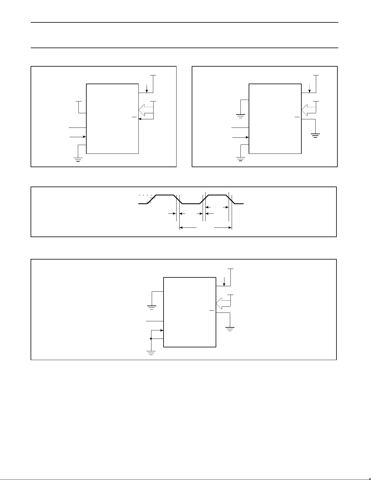
Figure 13. ICC Test Condition, Active Mode
All other pins are disconnected
VCC–0.5
Figure 15. Clock Signal Waveform for ICC Tests in Active and Idle Modes
V
0.45V
P0
EA
V
CC
I
CC
CC
V
CC
SU00719
(NC)
CLOCK SIGNAL
RST
XTAL2
XTAL1
V
SS
V
EA
V
CC
I
CC
CC
V
CC
P0
SU00720
Figure 14. ICC Test Condition, Idle Mode
All other pins are disconnected
0.7V
CC
0.2VCC–0.1
t
CHCL
t
CLCH
= t
t
CLCX
CHCL
t
CLCL
= 5ns
t
CHCX
t
CLCH
SU00009
V
CC
I
CC
V
CC
V
CC
P0
(NC)
RST
XTAL2
XTAL1
V
SS
EA
Figure 16. ICC Test Condition, Power Down Mode
All other pins are disconnected. V
= 2V to 5.5V
CC
SU00016
1996 Aug 16
20
Page 21
Philips Semiconductors Product specification
80C32/87C52CMOS single-chip 8-bit microcontrollers
EPROM CHARACTERISTICS
The 87C52 is programmed by using a modified Quick-Pulse
Programming algorithm. It differs from older methods in the value
used for V
number of the ALE/PROG
The 87C52 contains two signature bytes that can be read and used
by an EPROM programming system to identify the device. The
signature bytes identify the device as an 87C52 manufactured by
Philips.
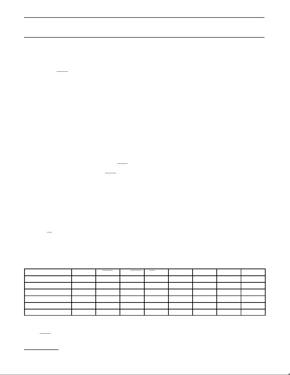
Table 6 shows the logic levels for reading the signature byte, and for
programming the program memory, the encryption table, and the
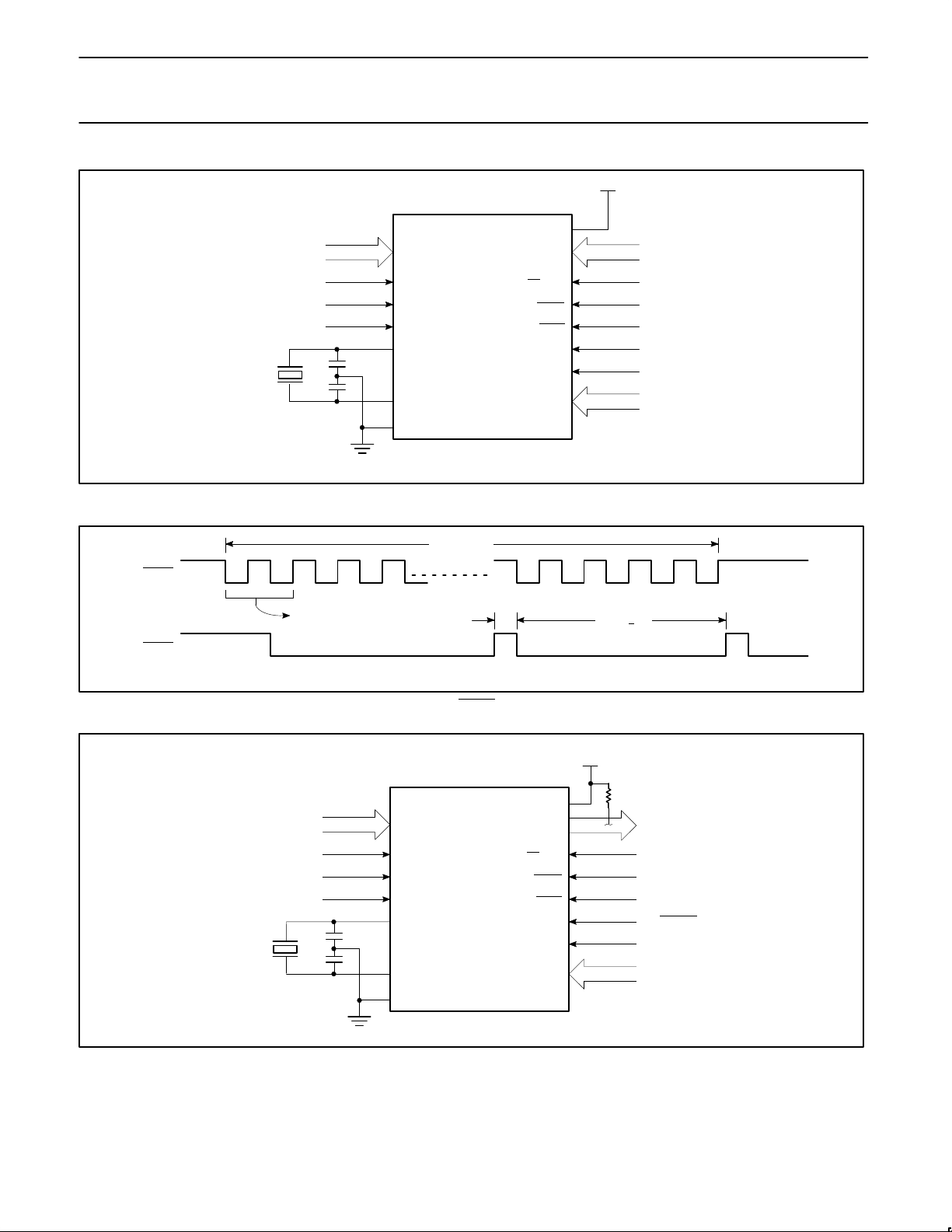
security bits. The circuit configuration and waveforms for quick-pulse
programming are shown in Figures 17 and 18. Figure 19 shows the
circuit configuration for normal program memory verification.
(programming supply voltage) and in the width and
PP
pulses.
Quick-Pulse Programming
The setup for microcontroller quick-pulse programming is shown in
Figure 17. Note that the 87C52 is running with a 4 to 6MHz
oscillator. The reason the oscillator needs to be running is that the
device is executing internal address and program data transfers.
The address of the EPROM location to be programmed is applied to
ports 1 and 2, as shown in Figure 17. The code byte to be
programmed into that location is applied to port 0. RST, PSEN
pins of ports 2 and 3 specified in Table 6 are held at the ‘Program
Code Data’ levels indicated in Table 6. The ALE/PROG
low 25 times as shown in Figure 18.
To program the encryption table, repeat the 25 pulse programming
sequence for addresses 0 through 1FH, using the ‘Pgm Encryption
Table’ levels. Do not forget that after the encryption table is
programmed, verification cycles will produce only encrypted data.
To program the security bits, repeat the 25 pulse programming
sequence using the ‘Pgm Security Bit’ levels. After one security bit is
programmed, further programming of the code memory and
encryption table is disabled. However, the other security bit can still
be programmed.
Note that the EA
maximum specified V
glitch above that voltage can cause permanent damage to the
device. The V
and overshoot.
/VPP pin must not be allowed to go above the
level for any amount of time. Even a narrow
PP
source should be well regulated and free of glitches
PP
and
is pulsed
Program Verification
If security bit 2 has not been programmed, the on-chip program
memory can be read out for program verification. The address of the
program memory locations to be read is applied to ports 1 and 2 as
shown in Figure 19. The other pins are held at the ‘Verify Code Data’
levels indicated in Table 6. The contents of the address location will
be emitted on port 0. External pull-ups are required on port 0 for this
operation.
If the encryption table has been programmed, the data presented at
port 0 will be the exclusive NOR of the program byte with one of the
encryption bytes. The user will have to know the encryption table
contents in order to correctly decode the verification data. The
encryption table itself cannot be read out.
Reading the Signature Bytes
The signature bytes are read by the same procedure as a normal
verification of locations 030H and 031H, except that P3.6 and P3.7
need to be pulled to a logic low. The values are:
(030H) = 15H indicates manufactured by Philips
(031H) = 97H indicates 87C52
Program/Verify Algorithms
Any algorithm in agreement with the conditions listed in Table 6, and
which satisfies the timing specifications, is suitable.
Erasure Characteristics
Erasure of the EPROM begins to occur when the chip is exposed to
light with wavelengths shorter than approximately 4,000 angstroms.
Since sunlight and fluorescent lighting have wavelengths in this
range, exposure to these light sources over an extended time (about
1 week in sunlight, or 3 years in room level fluorescent lighting)
could cause inadvertent erasure. For this and secondary effects,
it is recommended that an opaque label be placed over the
window. For elevated temperature or environments where solvents
are being used, apply Kapton tape Fluorglas part number 2345–5, or
equivalent.
The recommended erasure procedure is exposure to ultraviolet light
(at 2537 angstroms) to an integrated dose of at least 15W-s/cm
Exposing the EPROM to an ultraviolet lamp of 12,000µW/cm
for 20 to 39 minutes, at a distance of about 1 inch, should be
sufficient.
Erasure leaves the array in an all 1s state.
2
2
rating
.
Table 6. EPROM Programming Modes
MODE RST PSEN ALE/PROG EA/V
Read signature 1 0 1 1 0 0 0 0
Program code data 1 0 0* V
Verify code data 1 0 1 1 0 0 1 1
Pgm encryption table 1 0 0* V
Pgm security bit 1 1 0 0* V
Pgm security bit 2 1 0 0* V
NOTES:
1. ‘0’ = Valid low for that pin, ‘1’ = valid high for that pin.
= 12.75V ±0.25V.
2. V
PP
= 5V±10% during programming and verification.
3. V
CC
4. *ALE/PROG
minimum of 10µs.
Trademark phrase of Intel Corporation.
1996 Aug 16
receives 25 programming pulses while VPP is held at 12.75V . Each programming pulse is low for 100µs (±10µs) and high for a
21
PP
PP
PP
PP
PP
P2.7 P2.6 P3.7 P3.6
1 0 1 1
1 0 1 0
1 1 1 1
1 1 0 0
Page 22
Philips Semiconductors Product specification
80C32/87C52CMOS single-chip 8-bit microcontrollers
+5V
V
CC
A0–A7
P1
P0
PGM DATA
ALE/PROG:
ALE/PROG:
4–6MHz
1
1
1
RST
P3.6
P3.7
XTAL2
XTAL1
V
SS
87C52
EA
/V
PP
ALE/PROG
PSEN
P2.7
P2.6
P2.0–P2.4
+12.75V
25 100µs PULSES TO GROUND
0
1
0
A8–A12
SU00071
Figure 17. Programming Configuration
1
0
1
0
25 PULSES
100µs+1010µs MIN
SU00018
Figure 18. PROG Waveform
1996 Aug 16
4–6MHz
A0–A7
+5V
V
CC
/V
EA
PP
ALE/PROG
PSEN
P2.7
P2.6
P2.0–P2.4
P0
P1
1
1
1
RST
P3.6
P3.7
XTAL2
XTAL1
V
SS
87C52
PGM DATA
1
1
0
0 ENABLE
0
A8–A12
SU00072
Figure 19. Program Verification
22
Page 23
Philips Semiconductors Product specification
80C32/87C52CMOS single-chip 8-bit microcontrollers
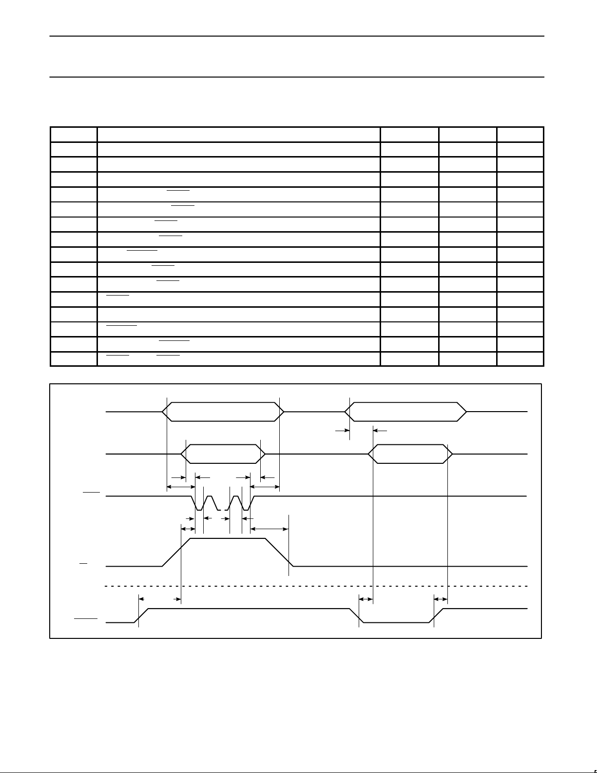
EPROM PROGRAMMING AND VERIFICATION CHARACTERISTICS
T
= 21°C to +27°C, VCC = 5V±10%, VSS = 0V (See Figure 20)
amb
SYMBOL
V
PP
I
PP
1/t
CLCL
t
AVGL
t
GHAX
t
DVGL
t
GHDX
t
EHSH
t
SHGL
t
GHSL
t
GLGH
t
AVQV
t
ELQZ
t
EHQZ
t
GHGL
Programming supply voltage 12.5 13.0 V
Programming supply current 50 mA
Oscillator frequency 4 6 MHz
Address setup to PROG low 48t
Address hold after PROG 48t
Data setup to PROG low 48t
Data hold after PROG 48t
P2.7 (ENABLE) high to V
VPP setup to PROG low 10 µs
VPP hold after PROG 10 µs
PROG width 90 110 µs
Address to data valid 48t
ENABLE low to data valid 48t
Data float after ENABLE 0 48t
PROG high to PROG low 10 µs
PARAMETER MIN MAX UNIT
CLCL
CLCL
CLCL
CLCL
PP
48t
CLCL
CLCL
CLCL
CLCL
P1.0–P1.7
P2.0–P2.4
PORT 0
t
DVGL
t
ALE/PROG
EA/V
P2.7
ENABLE
PP
AVGL
t
EHSH
t
GLGH
t
SHGL
NOTE:
*
FOR PROGRAMMING VERIFICATION SEE FIGURE 17.
FOR VERIFICATION CONDITIONS SEE FIGURE 19.
PROGRAMMING* VERIFICATION*
ADDRESS ADDRESS
t
AVQV
DATA IN DATA OUT
t
GHDX
t
GHAX
t
GHGL
LOGIC 0
t
GHSL
LOGIC 1 LOGIC 1
t
ELQV
Figure 20. EPROM Programming and Verification
t
EHQZ
SU00020
1996 Aug 16
23
Page 24
Philips Semiconductors Product specification
80C32/87C52CMOS single-chip 8-bit microcontrollers
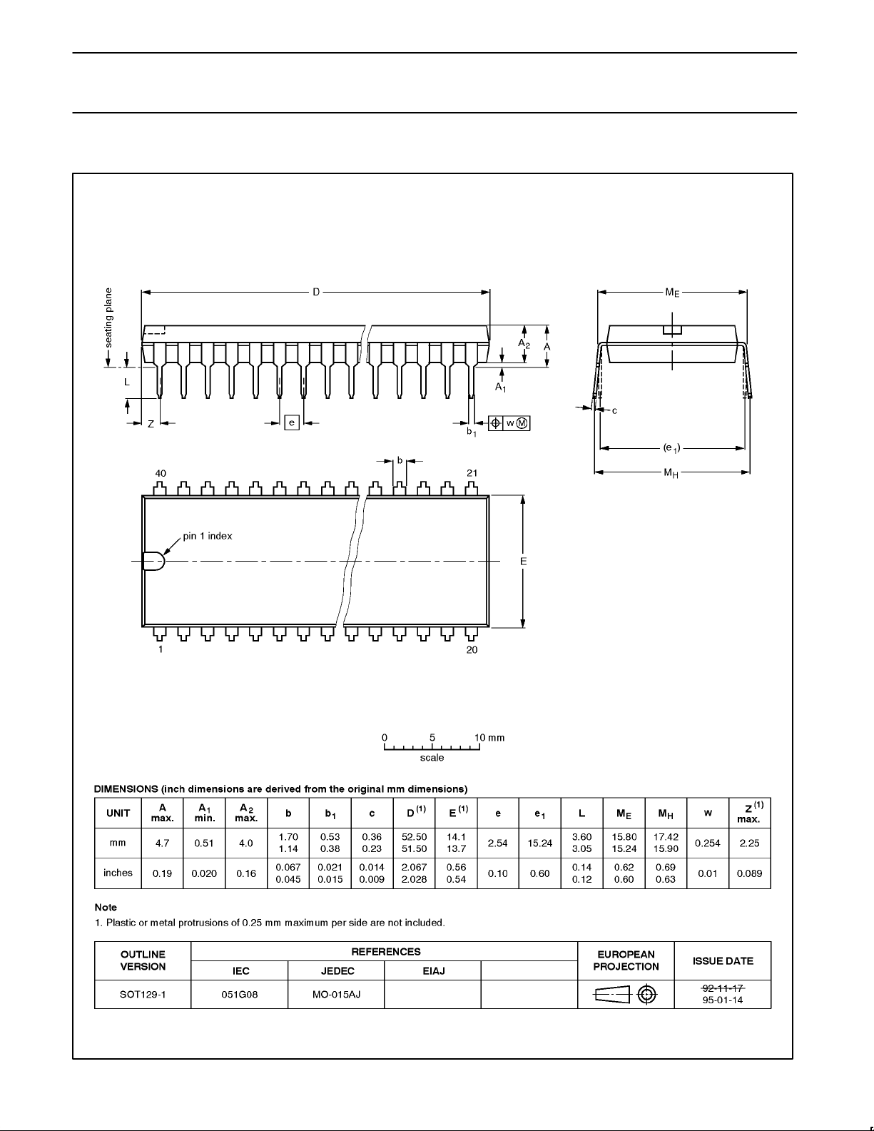
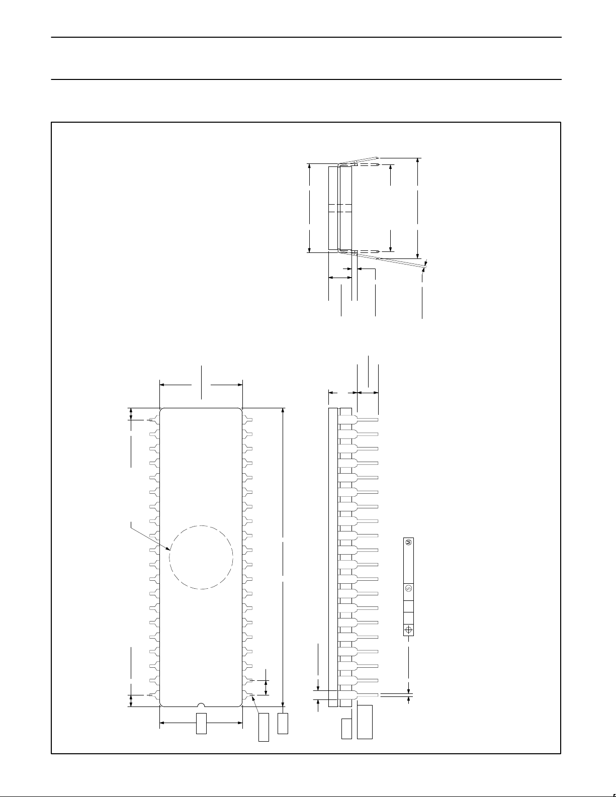
DIP40: plastic dual in-line package; 40 leads (600 mil) SOT129-1
1996 Aug 16
24
Page 25
Philips Semiconductors Product specification
80C32/87C52CMOS single-chip 8-bit microcontrollers
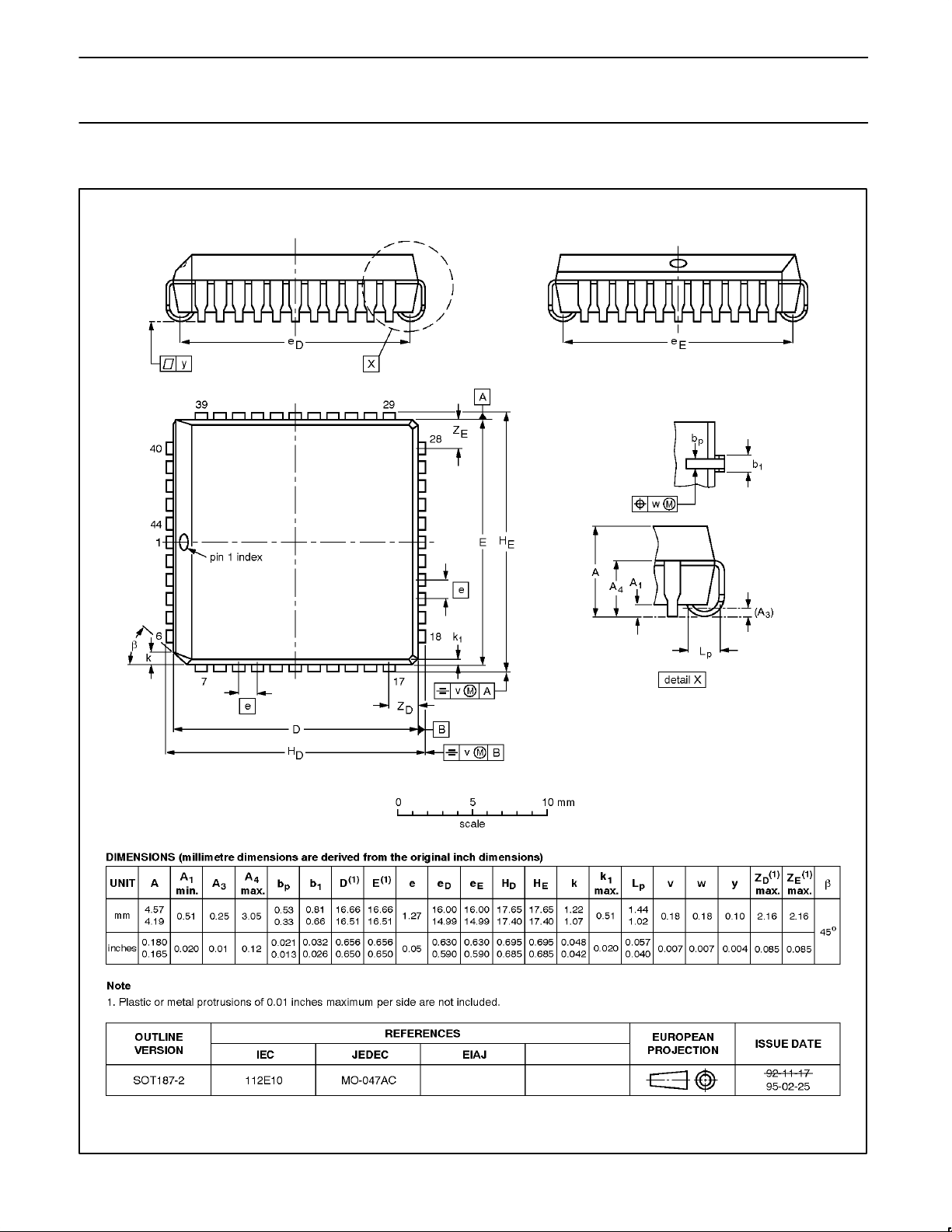
PLCC44: plastic leaded chip carrier; 44 leads SOT187-2
1996 Aug 16
25
Page 26
Philips Semiconductors Product specification
80C32/87C52CMOS single-chip 8-bit microcontrollers
0590B 40-PIN (600 mils wide) CERAMIC DUAL IN-LINE (F) PACKAGE (WITH WINDOW (FA) PACKAGE)
and include allowance for glass overrun and meniscus
on the seal line, and lid to base mismatch.
constrained to be perpendicular to plane T.
shown in parentheses.
NOTES:
1. Controlling dimension: Inches. Millimeters are
2. Dimension and tolerancing per ANSI Y14. 5M-1982.
3. “T”, “D”, and “E” are reference datums on the body
0.098 (2.49)
0.040 (1.02)
counterclockwise to Pin #40 when viewed
from the top.
4. These dimensions measured with the leads
5. Pin numbers start with Pin #1 and continue
6. Denotes window location for EPROM products.
0.598 (15.19)
0.571 (14.50)
(NOTE 4)
0.620 (15.75)
0.590 (14.99)
0.175 (4.45)
0.145 (3.68)
0.055 (1.40)
0.165 (4.19)
0.225 (5.72) MAX.
BSC
0.600 (15.24)
0.020 (0.51)
0.125 (3.18)
(NOTE 4)
0.695 (17.65)
0.600 (15.24)
0.015 (0.38)
0.010 (0.25)
SEE NOTE 6
0.098 (2.49)
853–0590B 06688
1996 Aug 16
0.040 (1.02)
– E –
2.087 (53.01)
2.038 (51.77)
0.100 (2.54) BSC
– D –
PIN # 1
26
0.070 (1.78)
0.050 (1.27)
0.010 (0.254)TED
0.023 (0.58)
0.015 (0.38)
PLANE
SEATING
– T –
Page 27
Philips Semiconductors Product specification
80C32/87C52CMOS single-chip 8-bit microcontrollers
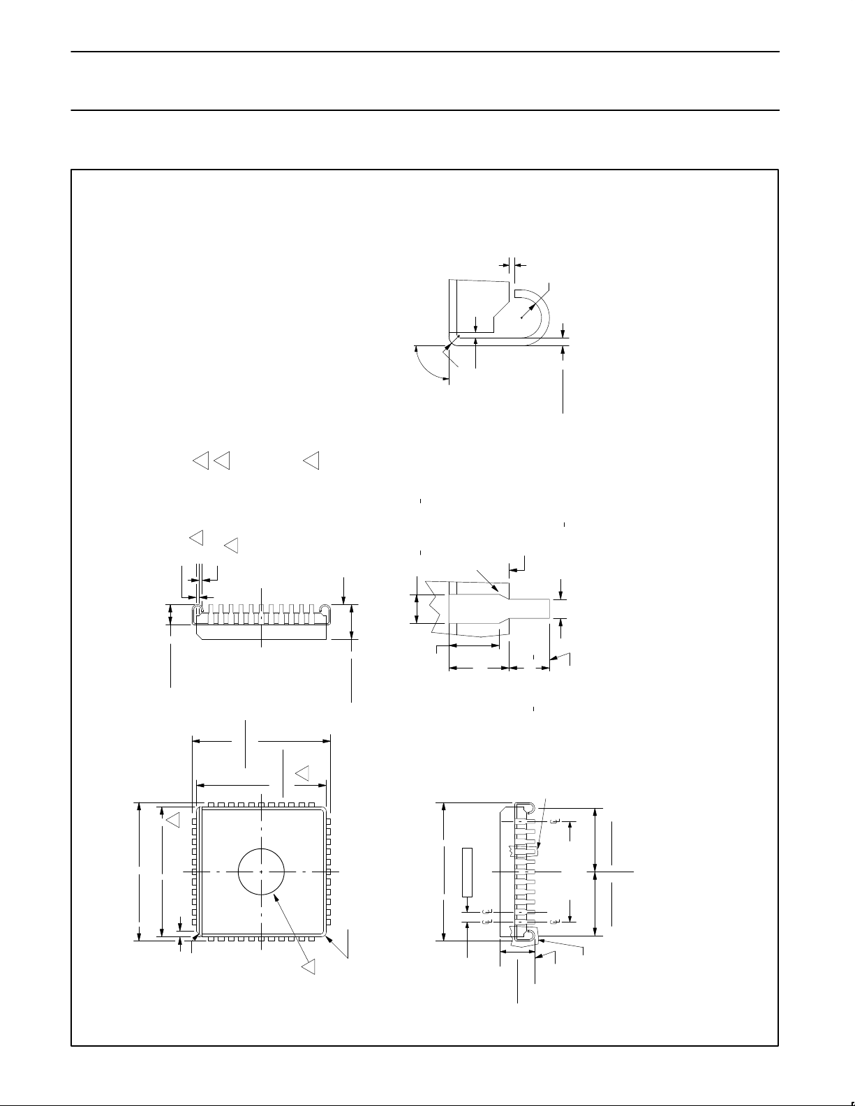
1472A 44-PIN CERQUAD J-BEND (K) PACKAGE
Glass protrusion to be 0.005 inches maximum
to ANSI Y14.5–1982.
NOTES:
1. All dimensions and tolerances to conform
2. UV window is optional.
6
0.38 (0.015)
on each side.
3. Dimensions do not include glass protrusion.
6
0.51 (0.02) X 45°
lead trim offset and lead plating finish.
dimensions are for reference only.
4. Controlling dimension millimeters.
5. All dimensions and tolerances include
6. Backside solder relief is optional and
SEATING
PLANE
0.076 (0.003) MIN.
°
–10
°°
90 + 5
0.15 (0.006) MIN.
0.25 (0.010) R MIN.
°
45 TYP.
0.73 + 0.08 (0.029 + 0.003)
4 PLACES
0.508 (0.020) R MIN.
0.25 (0.010)
BASE PLANE
0.482 (0.019 + 0.002)
DETAIL B
mm/(inch)
0.15 (0.006)
DETAIL A
TYP. ALL SIDES
mm/(inch)
3.05 (0.120)
2.29 (0.090)
3
16.89 (0.665)
16.00 (0.630)
17.65 (0.695)
17.40 (0.685)
1.02 (0.040) X 45°
853-1472A 05854
1996 Aug 16
45
CHAMFER
17.65 (0.695)
17.40 (0.685)
16.89 (0.665)
3
16.00 (0.630)
2
4.83 (0.190)
3.94 (0.155)
3 X 0.63 (0.025) R MIN.
27
1.27 (0.050) TYP.
17.65 (0.656)
17.40 (0.685)
1.27 (0.050)
1.52 (0.060) REF.
40X
SEATING
PLANE
1.02 + 0.25 (0.040 + 0.010)
SEE DETAIL A
NOMINAL
12.7 (0.500)
4.83 (0.190)
3.94 (0.155)
SEATING
PLANE
SEE DETAIL B
8.13 (0.320)
7.37 (0.290)
8.13 (0.320)
7.37 (0.290)
Page 28
Philips Semiconductors Product specification
80C32/87C52CMOS single-chip 8-bit microcontrollers
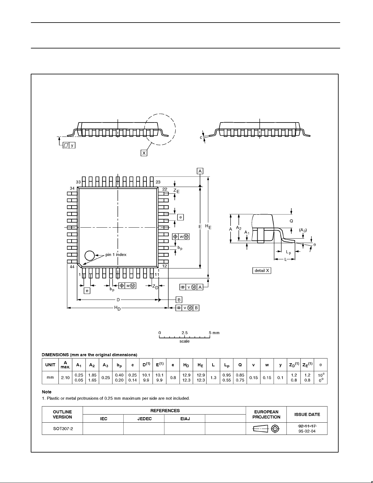
QFP44: plastic quad flat package; 44 leads (lead length 1.3 mm); body 10 x 10 x 1.75 mm SOT307-2
1996 Aug 16
28
Page 29

Philips Semiconductors Product specification
80C32/87C52CMOS single-chip 8-bit microcontrollers
NOTES
1996 Aug 16
29
Page 30

Philips Semiconductors Product specification
80C32/87C52CMOS single-chip 8-bit microcontrollers
DEFINITIONS
Data Sheet Identification Product Status Definition
Objective Specification
Preliminary Specification
Product Specification
Formative or in Design
Preproduction Product
Full Production
Philips Semiconductors and Philips Electronics North America Corporation reserve the right to make changes, without notice, in the products,
including circuits, standard cells, and/or software, described or contained herein in order to improve design and/or performance. Philips
Semiconductors assumes no responsibility or liability for the use of any of these products, conveys no license or title under any patent, copyright,
or mask work right to these products, and makes no representations or warranties that these products are free from patent, copyright, or mask
work right infringement, unless otherwise specified. Applications that are described herein for any of these products are for illustrative purposes
only. Philips Semiconductors makes no representation or warranty that such applications will be suitable for the specified use without further testing
or modification.
LIFE SUPPORT APPLICA TIONS
Philips Semiconductors and Philips Electronics North America Corporation Products are not designed for use in life support appliances, devices,
or systems where malfunction of a Philips Semiconductors and Philips Electronics North America Corporation Product can reasonably be expected
to result in a personal injury. Philips Semiconductors and Philips Electronics North America Corporation customers using or selling Philips
Semiconductors and Philips Electronics North America Corporation Products for use in such applications do so at their own risk and agree to fully
indemnify Philips Semiconductors and Philips Electronics North America Corporation for any damages resulting from such improper use or sale.
Philips Semiconductors
811 East Arques Avenue
P.O. Box 3409
Sunnyvale, California 94088–3409
Telephone 800-234-7381
This data sheet contains the design target or goal specifications for product development. Specifications
may change in any manner without notice.
This data sheet contains preliminary data, and supplementary data will be published at a later date. Philips
Semiconductors reserves the right to make changes at any time without notice in order to improve design
and supply the best possible product.
This data sheet contains Final Specifications. Philips Semiconductors reserves the right to make changes
at any time without notice, in order to improve design and supply the best possible product.
Philips Semiconductors and Philips Electronics North America Corporation
register eligible circuits under the Semiconductor Chip Protection Act.
Copyright Philips Electronics North America Corporation 1996
All rights reserved. Printed in U.S.A.
Page 31

INTEGRATED CIRCUITS
80C52/80C54/80C58
CMOS single-chip 8-bit microcontrollers
Product specification 1996 Aug 16
IC20 Data Handbook
Page 32
Philips Semiconductors Product specification
80C52/80C54/80C58CMOS single-chip 8-bit microcontrollers
DESCRIPTION
The 80C52/80C54/80C58 Single-Chip 8-Bit Microcontroller is
manufactured in an advanced CMOS process and is a derivative of
the 80C51 m ic r oc o n t ro l l e r fam i l y. The 80C52/80C54/80C58 has the
same instruction set as the 80C51.
This device provides architectural enhancements that make it
applicable in a variety of applications for general control systems.
The 80C52 contains 8k × 8 ROM memory, the 80C54 contains
16k × 8 ROM memory, and 80C58 contains 32k × 8 ROM memory, a
volatile 256 × 8 read/write data memory, four 8-bit I/O ports, three
16-bit timer/event counters, a multi-source, four-priority-level, nested
interrupt structure, an enhanced UART and on-chip oscillator and
timing circuits. For systems that require extra capability, the
80C52/54/58 can be expanded using standard TTL compatible
memories and logic.
Its added features make it an even more powerful microcontroller for
applications that require pulse width modulation, high-speed I/O and
up/down counting capabilities such as motor control. It also has a
more versatile serial channel that facilitates multiprocessor
communications.
See 87C52/80C32 and 87C54/87C58 data sheets for EPROM and
ROMless devices.
FEATURES
•80C51 central processing unit
•Full static operation
•8k × 8 ROM: 80C52;
16k × 8 ROM: 80C54;
32k × 8 ROM: 80C58;
all capable of addressing external memory to 64k bytes
– Two level program security system
– 64 byte encryption array
•256 × 8 RAM, expandable externally to 64k bytes
•Speed range up to 33MHz
•Operating voltage 5V ±10%
•Three 16-bit timer/counters
– T2 is an up/down counter
•6 interrupt sources
•4 level priority
•Four 8-bit I/O ports
•Full-duplex enhanced UART
– Framing error detection
– Automatic address recognition
•Power control modes
– Idle mode
– Power-down mode
•Once (On Circuit Emulation) Mode
•Five package styles
•Programmable clock out
•Low EMI (Inhibit ALE)
•Second DPTR register
•Asynchronous port reset
PIN CONFIGURATIONS
T2/P1.0
1
T2EX/P1.1
INT0
INT1
P1.2
P1.3
P1.4
P1.5
P1.6
P1.7
RST
RxD/P3.0
TxD/P3.1
/P3.2
/P3.3
T0/P3.4
T1/P3.5
/P3.6
WR
RD
/P3.7
XTAL2
XTAL1
V
SS
2
3
4
5
6
7
8
9
10
11
12
13
14
15
16
17
18
19
20
DUAL
IN-LINE
PACKAGE
40
39
38
37
36
35
34
33
32
31
30
29
28
27
26
25
24
23
22
21
V
CC
P0.0/AD0
P0.1/AD1
P0.2/AD2
P0.3/AD3
P0.4/AD4
P0.5/AD5
P0.6/AD6
P0.7/AD7
EA
ALE
PSEN
P2.7/A15
P2.6/A14
P2.5/A13
P2.4/A12
P2.3/A11
P2.2/A10
P2.1/A9
P2.0/A8
SU00740
1996 Aug 16 853–1470 17196
2
Page 33
Philips Semiconductors Product specification
80C52/80C54/80C58CMOS single-chip 8-bit microcontrollers
ORDERING INFORMATION
ROM
8k × 8
P80C52EBPN P80C54EBPN P80C58EBPN 0 to +70, Plastic Dual In-line Package 16 SOT129-1
P80C52EBAA P80C54EBAA P80C58EBAA 0 to +70, Plastic Leaded Chip Carrier 16 SOT187-2
P80C52EBBB P80C54EBBB P80C58EBBB 0 to +70, Plastic Quad Flat Pack 16 SOT307-2
P80C52EFPN P80C54EFPN P80C58EFPN –40 to +85, Plastic Dual In-line Package 16 SOT129-1
P80C52EFAA P80C54EFAA P80C58EFAA –40 to +85, Plastic Leaded Chip Carrier 16 SOT187-2
P80C52EFBB P80C54EFBB P80C58EFBB –40 to +85, Plastic Quad Flat Pack 16 SOT307-2
P80C52IBP N P80C54IBP N P80C58IBP N 0 to +70, Plastic Dual In-line Package 24 SOT129-1
P80C52IBA A P80C54IBA A P80C58IBA A 0 to +70, Plastic Leaded Chip Carrier 24 SOT187-2
P80C52IBB B P80C54IBB B P80C58IBB B 0 to +70, Plastic Quad Flat Pack 24 SOT307-2
P80C52IFP N P80C54IFP N P80C58IFP N –40 to +85, Plastic Dual In-line Package 24 SOT129-1
P80C52IFA A P80C54IFA A P80C58IFA A –40 to +85, Plastic Leaded Chip Carrier 24 SOT187-2
P80C52IFB B P80C54IFB B P80C58IFB B –40 to +85, Plastic Quad Flat Pack 24 SOT307-2
P80C52NBAA P80C54NBAA P80C58NBAA 0 to +70, Plastic Leaded Chip Carrier 33 SOT187-2
P80C52NBPN P80C54NBPN P80C58NBPN 0 to +70, Plastic Dual In-line Package 33 SOT129-1
P80C52NBBB P80C54NBBB P80C58NBBB 0 to +70, Plastic Quad Flat Pack 33 SOT307-2
P80C52NFAA P80C54NFAA P80C58NFAA –40 to +85, Plastic Leaded Chip Carrier 33 SOT187-2
P80C52NFPN P80C54NFPN P80C58NFPN –40 to +85, Plastic Dual In-line Package 33 SOT129-1
P80C52NFBB P80C54NFBB P80C58NFBB –40 to +85, Plastic Quad Flat Pack 33 SOT307-2
ROM
16k × 8
ROM
32k × 8
TEMPERATURE RANGE °C
AND PACKAGE
FREQ
MHz
DRAWING
NUMBER
LOGIC SYMBOL
RST
PSEN
RxD
TxD
INT0
INT1
T0
T1
WR
RD
SECONDARY FUNCTIONS
XTAL1
XTAL2
EA
ALE
PORT 3
V
V
SS
CC
ADDRESS AND
PORT 0
DATA BUS
T2
T2EX
PORT 1PORT 2
ADDRESS BUS
SU00732
1996 Aug 16
3
Page 34
Philips Semiconductors Product specification
80C52/80C54/80C58CMOS single-chip 8-bit microcontrollers
BLOCK DIAGRAM
P0.0–P0.7 P2.0–P2.7
PSEN
ALE
EA
RST
PORT 0
DRIVERS
V
CC
V
SS
RAM ADDR
REGISTER
B
REGISTER
TIMING
AND
CONTROL
INSTRUCTION
PD
REGISTER
RAM
ACC
TMP2
PORT 1
LATCH
PSW
PORT 0
LATCH
ALU
8
TMP1
PORT 2
DRIVERS
PORT 2
LATCH
SFRs
TIMERS
8
POINTER
STACK
PORT 3
LATCH
ROM
16
PROGRAM
ADDRESS
REGISTER
BUFFER
PC
INCRE-
MENTER
8 16
PROGRAM
COUNTER
MULTIPLE
DPTRs
OSCILLATOR
XTAL1 XTAL2
1996 Aug 16
PORT 1
DRIVERS
P1.0–P1.7
PORT 3
DRIVERS
P3.0–P3.7
SU00733B
4
Page 35
Philips Semiconductors Product specification
80C52/80C54/80C58CMOS single-chip 8-bit microcontrollers
Table 1. 80C52/80C54/80C58 Special Function Registers
SYMBOL DESCRIPTION
ACC* Accumulator E0H E7 E6 E5 E4 E3 E2 E1 E0 00H
AUXR# Auxiliary 8EH – – – – – – – AO xxxxxxx0B
AUXR1# Auxiliary 1 A2H – – – – – – – DPS xxxxxxx0B
B* B register F0H F7 F6 F5 F4 F3 F2 F1 F0 00H
DPTR: Data Pointer (2 bytes)
DPH Data Pointer High 83H 00H
DPL Data Pointer Low 82H 00H
IE* Interrupt Enable A8H EA EC ET2 ES ET1 EX1 ET0 EX0 00H
IP* Interrupt Priority B8H – – PT2 PS PT1 PX1 PT0 PX0 x0000000B
IPH# Interrupt Priority High B7H – – PT2H PSH PT1H PX1H PT0H PX0H x0000000B
P0* Port 0 80H AD7 AD6 AD5 AD4 AD3 AD2 AD1 AD0 FFH
P1* Port 1 90H – – – – – – T2EX T2 FFH
P2* Port 2 A0H AD15 AD14 AD13 AD12 AD11 AD10 AD9 AD8 FFH
P3* Port 3 B0H RD WR T1 T0 INT1 INT0 TxD RxD FFH
DIRECT
ADDRESS
BIT ADDRESS, SYMBOL, OR ALTERNATIVE PORT FUNCTION
MSB LSB
AF AE AD AC AB AA A9 A8
BF BE BD BC BB BA B9 B8
B7 B6 B5 B4 B3 B2 B1 B0
87 86 85 84 83 82 81 80
97 96 95 94 93 92 91 90
A7 A6 A5 A4 A3 A2 A1 A0
B7 B6 B5 B4 B3 B2 B1 B0
RESET
VALUE
1
PCON#
PSW* Program Status Word D0H CY AC F0 RS1 RS0 OV – P 00H
RACAP2H
RACAP2L
SADDR# Slave Address A9H 00H
SADEN# Slave Address Mask B9H 00H
SBUF Serial Data Buffer 99H xxxxxxxxB
SCON* Serial Control 98H
SP Stack Pointer 81H 07H
TCON* Timer Control 88H TF1 TR1 TF0 TR0 IE1 IT1 IE0 IT0 00H
T2CON* Timer 2 Control C8H TF2 EXF2 RCLK TCLK EXEN2 TR2 C/T2 CP/RL2 00H
T2MOD# Timer 2 Mode Control C9H – – – – – – T2OE DCEN xxxxxx00B
TH0 Timer High 0 8CH 00H
TH1 Timer High 1 8DH 00H
TH2# Timer High 2 CDH 00H
TL0 Timer Low 0 8AH 00H
TL1 Timer Low 1 8BH 00H
TL2# Timer Low 2 CCH 00H
TMOD Timer Mode 89H GATE C/T M1 M0 GATE C/T M1 M0 00H
* SFRs are bit addressable.
# SFRs are modified from or added to the 80C51 SFRs.
– Reserved bits.
1. Reset value depends on reset source.
2. Bit will not be affected by Reset. POF is not present in 80C52.
Power Control 87H
# Timer 2 Capture High CBH 00H
# Timer 2 Capture Low CAH 00H
SMOD1 SMOD0
D7 D6 D5 D4 D3 D2 D1 D0
9F 9E 9D 9C 9B 9A 99 98
SM0/FE
8F 8E 8D 8C 8B 8A 89 88
CF CE CD CC CB CA C9 C8
SM1 SM2 REN TB8 RB8 TI RI 00H
– POF
2
GF1 GF0 PD IDL 00xx0000B
1996 Aug 16
5
Page 36
Philips Semiconductors Product specification
80C52/80C54/80C58CMOS single-chip 8-bit microcontrollers
PLASTIC LEADED CHIP CARRIER PIN FUNCTIONS
6140
Pin Function
1 NC*
2 P1.0/T2
3 P1.1/T2EX
4 P1.2
5 P1.3
6 P1.4
7 P1.5
8 P1.6
9 P1.7
10 RST
11 P3.0/RxD
12 NC*
13 P3.1/TxD
14 P3.2/INT0
15 P3.3/INT1
* DO NOT CONNECT
7
17
18 28
Pin Function
16 P3.4/T0
17 P3.5/T1
18 P3.6/WR
19 P3.7/RD
20 XTAL2
21 XTAL1
22 V
23 NC*
24 P2.0/A8
25 P2.1/A9
26 P2.2/A10
27 P2.3/A11
28 P2.4/A12
29 P2.5/A13
30 P2.6/A14
LCC
SS
39
29
Pin Function
31 P2.7/A15
32 PSEN
33 ALE
34 NC*
35 EA
36 P0.7/AD7
37 P0.6/AD6
38 P0.5/AD5
39 P0.4/AD4
40 P0.3/AD3
41 P0.2/AD2
42 P0.1/AD1
43 P0.0/AD0
44 V
CC
SU00741A
PLASTIC QUAD FLAT PACK PIN FUNCTIONS
44 34
Pin Function
1 P1.5
2 P1.6
3 P1.7
4 RST
5 P3.0/RxD
6 NC*
7 P3.1/TxD
8 P3.2/INT0
9 P3.3/INT1
10 P3.4/T0
11 P3.5/T1
12 P3.6/WR
13 P3.7/RD
14 XTAL2
15 XTAL1
* DO NOT CONNECT
1
11
PQFP
12 22
Pin Function
16 V
SS
17 NC*
18 P2.0/A8
19 P2.1/A9
20 P2.2/A10
21 P2.3/A11
22 P2.4/A12
23 P2.5/A13
24 P2.6/A14
25 P2.7/A15
26 PSEN
27 ALE
28 NC*
29 EA
30 P0.7/AD7
33
23
Pin Function
31 P0.6/AD6
32 P0.5/AD5
33 P0.4/AD4
34 P0.3/AD3
35 P0.2/AD2
36 P0.1/AD1
37 P0.0/AD0
38 V
CC
39 NC*
40 P1.0/T2
41 P1.1/T2EX
42 P1.2
43 P1.3
44 P1.4
SU00742A
PIN DESCRIPTIONS
PIN NUMBER
MNEMONIC DIP LCC QFP TYPE NAME AND FUNCTION
V
SS
V
CC
P0.0–0.7 39–32 43–36 37–30 I/O Port 0: Port 0 is an open-drain, bidirectional I/O port. Port 0 pins that have 1s written to
P1.0–P1.7 1–8 2–9 40–44,
P2.0–P2.7 21–28 24–31 18–25 I/O Port 2: Port 2 is an 8-bit bidirectional I/O port with internal pull-ups. Port 2 pins that have 1s
20 22 16 I Ground: 0V reference.
40 44 38 I Power Supply: This is the power supply voltage for normal, idle, and power-down
operation.
them float and can be used as high-impedance inputs. Port 0 is also the multiplexed
low-order address and data bus during accesses to external program and data memory. In
this application, it uses strong internal pull-ups when emitting 1s. Port 0 also outputs the
code bytes during program verification. External pull-ups are required during program
verification.
I/O Port 1: Port 1 is an 8-bit bidirectional I/O port with internal pull-ups. Port 1 pins that have 1s
1–3
written to them are pulled high by the internal pull-ups and can be used as inputs. As inputs,
port 1 pins that are externally pulled low will source current because of the internal pull-ups.
(See DC Electrical Characteristics: I
during program memory verification. Alternate functions include:
). Port 1 also receives the low-order address byte
IL
1 2 40 I/O T2 (P1.0): Timer/Counter 2 external count input/Clockout
2 3 41 I T2EX (P1.1): Timer/Counter 2 Reload/Capture/Direction Control
3 4 42 I
4 5 43 I/O
5 6 44 I/O
6 7 1 I/O
7 8 2 I/O
8 9 3 I/O
written to them are pulled high by the internal pull-ups and can be used as inputs. As inputs,
port 2 pins that are externally being pulled low will source current because of the internal
pull-ups. (See DC Electrical Characteristics: I
during fetches from external program memory and during accesses to external data memory
). Port 2 emits the high-order address byte
IL
that use 16-bit addresses (MOVX @DPTR). In this application, it uses strong internal
pull-ups when emitting 1s. During accesses to external data memory that use 8-bit
addresses (MOV @Ri), port 2 emits the contents of the P2 special function register.
1996 Aug 16
6
Page 37
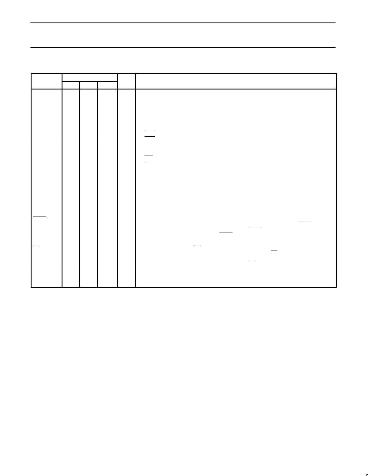
Philips Semiconductors Product specification
80C52/80C54/80C58CMOS single-chip 8-bit microcontrollers
PIN DESCRIPTIONS (Continued)
PIN NUMBER
MNEMONIC DIP LCC QFP TYPE NAME AND FUNCTION
P3.0–P3.7 10–17 11,
13–195,7–13
10 11 5 I RxD (P3.0): Serial input port
11 13 7 O TxD (P3.1): Serial output port
12 14 8 I INT0 (P3.2): External interrupt
13 15 9 I INT1 (P3.3): External interrupt
14 16 10 I T0 (P3.4): Timer 0 external input
15 17 11 I T1 (P3.5): Timer 1 external input
16 18 12 O WR (P3.6): External data memory write strobe
17 19 13 O RD (P3.7): External data memory read strobe
RST 9 10 4 I Reset: A high on this pin for two machine cycles while the oscillator is running, resets the
ALE 30 33 27 O Address Latch Enable: Output pulse for latching the low byte of the address during an
PSEN 29 32 26 O Program Store Enable: The read strobe to external program memory . When the
EA 31 35 29 I External Access Enable: EA must be externally held low to enable the device to fetch code
XTAL1 19 21 15 I Crystal 1: Input to the inverting oscillator amplifier and input to the internal clock generator
XTAL2 18 20 14 O Crystal 2: Output from the inverting oscillator amplifier.
NOTE:
To avoid “latch-up” effect at power-on, the voltage on any pin at any time must not be higher than V
I/O Port 3: Port 3 is an 8-bit bidirectional I/O port with internal pull-ups. Port 3 pins that have 1s
written to them are pulled high by the internal pull-ups and can be used as inputs. As inputs,
port 3 pins that are externally being pulled low will source current because of the pull-ups.
(See DC Electrical Characteristics: I
family, as listed below:
device. An internal diffused resistor to V
capacitor to V
access to external memory. In normal operation, ALE is emitted at a constant rate of 1/6 the
oscillator frequency , and can be used for external timing or clocking. Note that one ALE
pulse is skipped during each access to external data memory. ALE can be disabled by
setting SFR auxiliary.0. With this bit set, ALE will be active only during a MOVX instruction.
80C52/80C54/80C58 is executing code from the external program memory, PSEN
activated twice each machine cycle, except that two PSEN
each access to external data memory. PSEN
program memory.
from external program memory locations 0000H and 7FFFH. If EA
executes from internal program memory unless the program counter contains an address
greater than 7FFFH. If security bit 1 is programmed, EA
circuits.
CC
.
). Port 3 also serves the special features of the 80C51
IL
permits a power-on reset using only an external
SS
is not activated during fetches from internal
CC
activations are skipped during
is held high, the device
will be internally latched on Reset.
+ 0.5V or VSS – 0.5V , respectively.
is
1996 Aug 16
7
Page 38
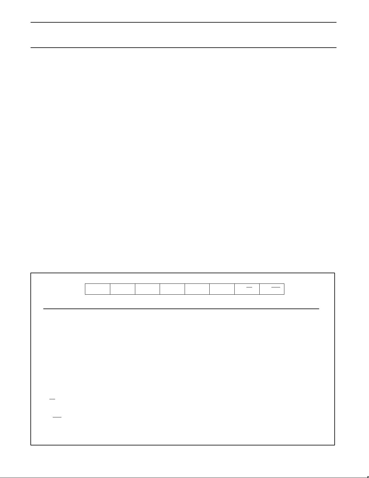
Philips Semiconductors Product specification
80C52/80C54/80C58CMOS single-chip 8-bit microcontrollers
TIMER 2 OPERATION
Timer 2
Timer 2 is a 16-bit Timer/Counter which can operate as either an
event timer or an event counter, as selected by C/T2* in the special
function register T2CON (see Figure 1). Timer 2 has three operating
modes:Capture, Auto-reload (up or down counting) ,and Baud Rate
Generator, which are selected by bits in the T2CON as shown in
Table 2.
Capture Mode
In the capture mode there are two options which are selected by bit
EXEN2 in T2CON. If EXEN2=0, then timer 2 is a 16-bit timer or
counter (as selected by C/T2* in T2CON) which, upon overflowing
sets bit TF2, the timer 2 overflow bit. This bit can be used to
generate an interrupt (by enabling the Timer 2 interrupt bit in the
IE register/SFR table). If EXEN2= 1, Timer 2 operates as described
above, but with the added feature that a 1- to -0 transition at external
input T2EX causes the current value in the Timer 2 registers, TL2
and TH2, to be captured into registers RCAP2L and RCAP2H,
respectively. In addition, the transition at T2EX causes bit EXF2 in
T2CON to be set, and EXF2 like TF2 can generate an interrupt
(which vectors to the same location as Timer 2 overflow interrupt.
The Timer 2 interrupt service routine can interrogate TF2 and EXF2
to determine which event caused the interrupt). The capture mode is
illustrated in Figure 2 (There is no reload value for TL2 and TH2 in
this mode. Even when a capture event occurs from T2EX, the
counter keeps on counting T2EX pin transitions or osc/12 pulses.).
Auto-Reload Mode (Up or Down Counter)
In the 16-bit auto-reload mode, Timer 2 can be configured (as either
a timer or counter (C/T2* in T2CON)) then programmed to count up
or down. The counting direction is determined by bit DCEN(Down
Counter Enable) which is located in the T2MOD register (see
Figure 3). When reset is applied the DCEN=0 which means Timer 2
will default to counting up. If DCEN bit is set, Timer 2 can count up
or down depending on the value of the T2EX pin.
Figure 4 shows Timer 2 which will count up automatically since
DCEN=0. In this mode there are two options selected by bit EXEN2
in T2CON register. If EXEN2=0, then T imer 2 counts up to 0FFFFH
and sets the TF2 (Overflow Flag) bit upon overflow. This causes the
Timer 2 registers to be reloaded with the 16-bit value in RCAP2L
and RCAP2H.
The values in RCAP2L and RCAP2H are preset by software means.
If EXEN2=1, then a 16-bit reload can be triggered either by an
overflow or by a 1-to-0 transition at input T2EX. This transition also
sets the EXF2 bit. The Timer 2 interrupt, if enabled, can be
generated when either TF2 or EXF2 are 1.
In Figure 5 DCEN=1 which enables Timer 2 to count up or down.
This mode allows pin T2EX to control the direction of count. When a
logic 1 is applied at pin T2EX Timer 2 will count up. Timer 2 will
overflow at 0FFFFH and set the TF2 flag, which can then generate
an interrupt, if the interrupt is enabled. This timer overflow also
causes the 16–bit value in RCAP2L and RCAP2H to be reloaded
into the timer registers TL2 and TH2.
When a logic 0 is applied at pin T2EX this causes Timer 2 to count
down. The timer will underflow when TL2 and TH2 become equal to
the value stored in RCAP2L and RCAP2H. Timer 2 underflow sets
the TF2 flag and causes 0FFFFH to be reloaded into the timer
registers TL2 and TH2.
The external flag EXF2 toggles when Timer 2 underflows or
overflows. This EXF2 bit can be used as a 17th bit of resolution if
needed. The EXF2 flag does not generate an interrupt in this mode
of operation.
(MSB) (LSB)
TF2 EXF2 RCLK TCLK EXEN2 TR2 C/T2
Symbol Position Name and Significance
TF2 T2CON.7 Timer 2 overflow flag set by a Timer 2 overflow and must be cleared by software. TF2 will not be set
EXF2 T2CON.6 Timer 2 external flag set when either a capture or reload is caused by a negative transition on T2EX and
RCLK T2CON.5 Receive clock flag. When set, causes the serial port to use Timer 2 overflow pulses for its receive clock
TCLK T2CON.4 Transmit clock flag. When set, causes the serial port to use Timer 2 overflow pulses for its transmit clock
EXEN2 T2CON.3 Timer 2 external enable flag. When set, allows a capture or reload to occur as a result of a negative
TR2 T2CON.2 Start/stop control for Timer 2. A logic 1 starts the timer.
C/T2
CP/RL2
T2CON.1 Timer or counter select. (Timer 2)
T2CON.0 Capture/Reload flag. When set, captures will occur on negative transitions at T2EX if EXEN2 = 1. When
when either RCLK or TCLK = 1.
EXEN2 = 1. When Timer 2 interrupt is enabled, EXF2 = 1 will cause the CPU to vector to the Timer 2
interrupt routine. EXF2 must be cleared by software. EXF2 does not cause an interrupt in up/down
counter mode (DCEN = 1).
in modes 1 and 3. RCLK = 0 causes Timer 1 overflow to be used for the receive clock.
in modes 1 and 3. TCLK = 0 causes Timer 1 overflows to be used for the transmit clock.
transition on T2EX if Timer 2 is not being used to clock the serial port. EXEN2 = 0 causes Timer 2 to
ignore events at T2EX.
0 = Internal timer (OSC/12)
1 = External event counter (falling edge triggered).
cleared, auto-reloads will occur either with Timer 2 overflows or negative transitions at T2EX when
EXEN2 = 1. When either RCLK = 1 or TCLK = 1, this bit is ignored and the timer is forced to auto-reload
on Timer 2 overflow .
Figure 1. Timer/Counter 2 (T2CON) Control Register
CP/RL2
SU00728
1996 Aug 16
8
Page 39
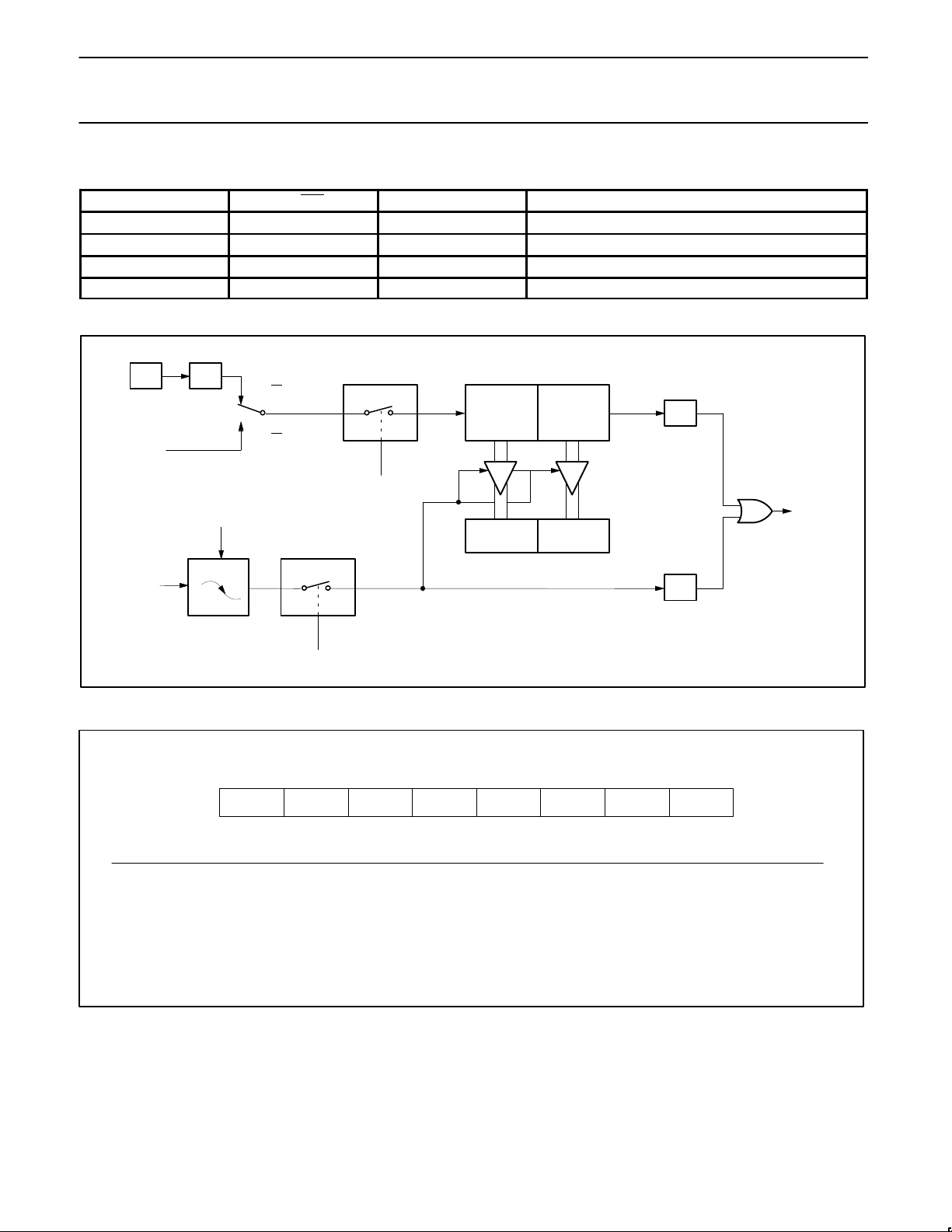
Philips Semiconductors Product specification
80C52/80C54/80C58CMOS single-chip 8-bit microcontrollers
Table 2. Timer 2 Operating Modes
RCLK + TCLK CP/RL2 TR2 MODE
0 0 1 16-bit Auto-reload
0 1 1 16-bit Capture
1 X 1 Baud rate generator
X X 0 (off)
OSC
T2 Pin
T2EX Pin
÷ 12
Transition
Detector
C/T2 = 0
C/T2
= 1
EXEN2
Control
TR2
Control
Capture
TL2
(8-bits)
RCAP2L RCAP2H
TH2
(8-bits)
TF2
EXF2
Figure 2. Timer 2 in Capture Mode
T2MOD Address = 0C9H Reset Value = XXXX XX00B
Not Bit Addressable
— — — — — — T2OE DCEN
Timer 2
Interrupt
SU00066
Bit
Symbol Function
— Not implemented, reserved for future use.*
T2OE Timer 2 Output Enable bit. See details in Programmable Clock-Out.
DCEN Down Count Enable bit. When set, this allows Timer 2 to be configured as an up/down counter.
* User software should not write 1s to reserved bits. These bits may be used in future 8051 family products to invoke new features.
In that case, the reset or inactive value of the new bit will be 0, and its active value will be 1. The value read from a reserved bit is
indeterminate.
1996 Aug 16
76543210
SU00746
Figure 3. Timer 2 Mode (T2MOD) Control Register
9
Page 40
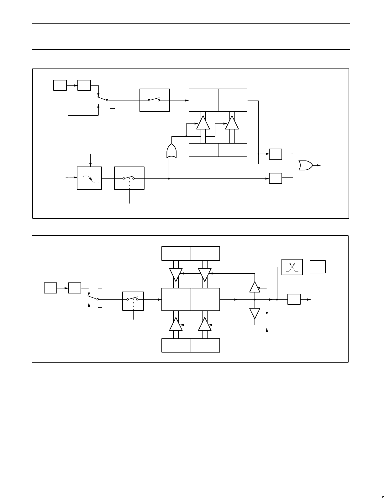
Philips Semiconductors Product specification
80C52/80C54/80C58CMOS single-chip 8-bit microcontrollers
OSC
T2 PIN
T2EX PIN
÷ 12
TRANSITION
DETECTOR
C/T2 = 0
= 1
C/T2
EXEN2
CONTROL
TR2
CONTROL
RELOAD
TL2
(8-BITS)
RCAP2L RCAP2H
TH2
(8-BITS)
Figure 4. Timer 2 in Auto-Reload Mode (DCEN = 0)
(DOWN COUNTING RELOAD VALUE)
FFH FFH
TF2
EXF2
TOGGLE
EXF2
TIMER 2
INTERRUPT
SU00067
OSC
T2 PIN
÷12
C/T2 = 0
C/T2
= 1
TL2 TH2
OVERFLOW
CONTROL
TR2
RCAP2L RCAP2H
(UP COUNTING RELOAD VALUE) T2EX PIN
Figure 5. Timer 2 Auto Reload Mode (DCEN = 1)
COUNT
DIRECTION
1 = UP
0 = DOWN
TF2
INTERRUPT
SU00730
1996 Aug 16
10
Page 41
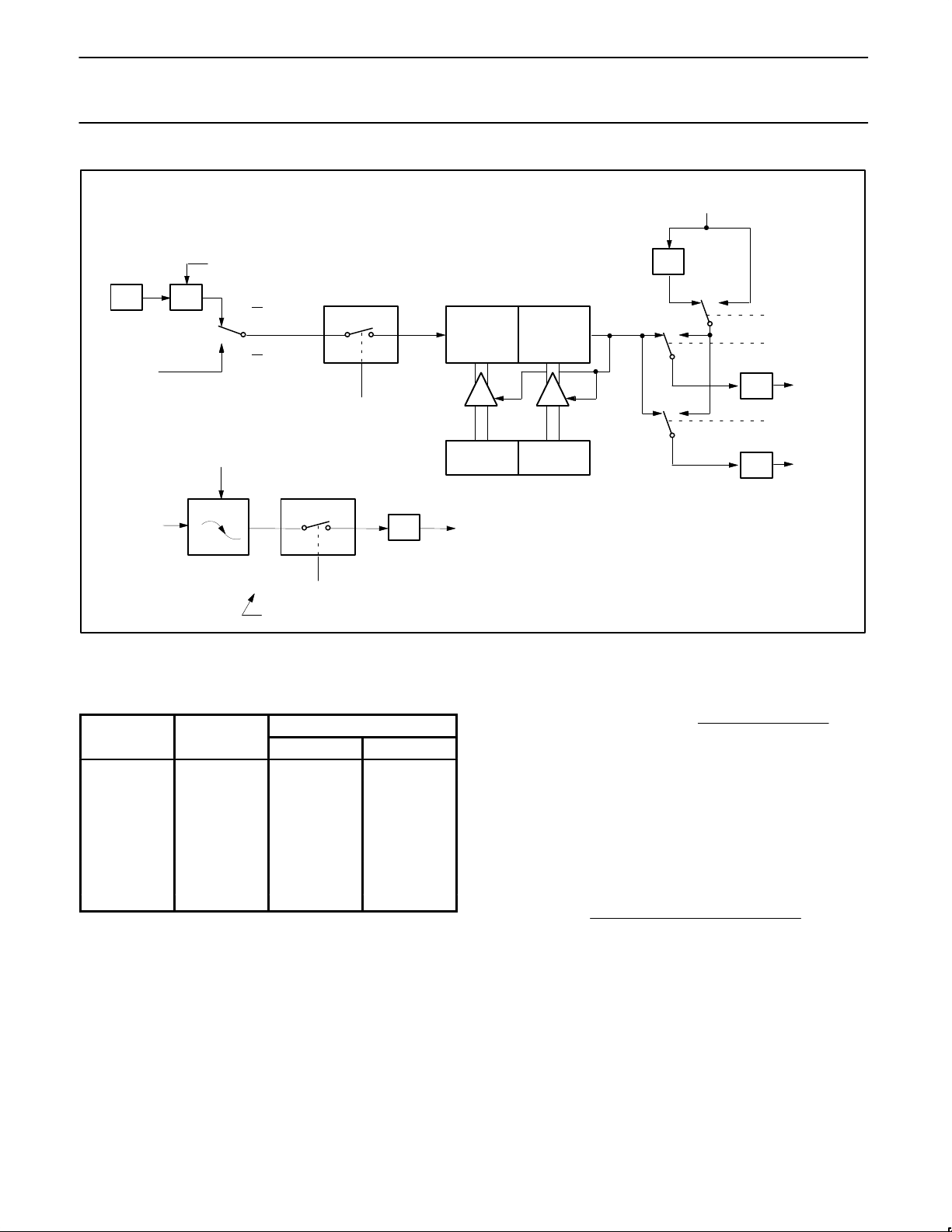
Philips Semiconductors Product specification
Baud Rat
O
80C52/80C54/80C58CMOS single-chip 8-bit microcontrollers
Timer 1
Overflow
NOTE: OSC. Freq. is divided by 2, not 12.
OSC
T2 Pin
T2EX Pin
÷ 2
Transition
Detector
C/T2 = 0
C/T2
= 1
EXEN2
Note availability of additional external interrupt.
Control
TR2
Control
EXF2
Figure 6. Timer 2 in Baud Rate Generator Mode
Table 3. Timer 2 Generated Commonly Used
Baud Rates
e
sc Freq
RCAP2H RCAP2L
375K 12MHz FF FF
9.6K 12MHz FF D9
2.8K 12MHz FF B2
2.4K 12MHz FF 64
1.2K 12MHz FE C8
300 12MHz FB 1E
110 12MHz F2 AF
300 6MHz FD 8F
110 6MHz F9 57
Timer 2
Baud Rate Generator Mode
Bits TCLK and/or RCLK in T2CON (Table 2) allow the serial port
transmit and receive baud rates to be derived from either Timer 1 or
Timer 2. When TCLK= 0, Timer 1 is used as the serial port transmit
baud rate generator . When TCLK= 1, Timer 2 is used as the serial
port transmit baud rate generator. RCLK has the same effect for the
serial port receive baud rate. With these two bits, the serial port can
have different receive and transmit baud rates – one generated by
Timer 1, the other by Timer 2.
Figure 6 shows the Timer 2 in baud rate generation mode. The baud
rate generation mode is like the auto-reload mode,in that a rollover
in TH2 causes the Timer 2 registers to be reloaded with the 16-bit
value in registers RCAP2H and RCAP2L, which are preset by
software.
÷ 2
“0” “1”
TL2
(8-bits)
RCAP2L RCAP2H
Timer 2
Interrupt
TH2
(8-bits)
Reload
“0”“1”
“0”“1”
SMOD
RCLK
÷ 16
TCLK
÷ 16 TX Clock
The baud rates in modes 1 and 3 are determined by Timer 2’s
overflow rate given below:
Modes 1 and 3 Baud Rates
Timer 2 Overflow Rate
16
The timer can be configured for either “timer” or “counter” operation.
In many applications, it is configured for “timer” operation (C/T2*=0).
Timer operation is different for Timer 2 when it is being used as a
baud rate generator.
Usually, as a timer it would increment every machine cycle (i.e., 1/12
the oscillator frequency). As a baud rate generator, it increments
every state time (i.e., 1/2 the oscillator frequency). Thus the baud
rate formula is as follows:
Modes 1 and 3 Baud Rates =
Oscillator Frequency
[32 [65536 (RCAP2H,RCAP2L)]]
Where: (RCAP2H, RCAP2L)= The content of RCAP2H and
RCAP2L taken as a 16-bit unsigned integer.
The Timer 2 as a baud rate generator mode shown in Figure 6, is
valid only if RCLK and/or TCLK = 1 in T2CON register. Note that a
rollover in TH2 does not set TF2, and will not generate an interrupt.
Thus, the Timer 2 interrupt does not have to be disabled when
Timer 2 is in the baud rate generator mode. Also if the EXEN2
(T2 external enable flag) is set, a 1-to-0 transition in T2EX
(Timer/counter 2 trigger input) will set EXF2 (T2 external flag) but
will not cause a reload from (RCAP2H, RCAP2L) to (TH2,TL2).
Therefore when Timer 2 is in use as a baud rate generator, T2EX
can be used as an additional external interrupt, if needed.
RX Clock
SU00068
1996 Aug 16
11
Page 42
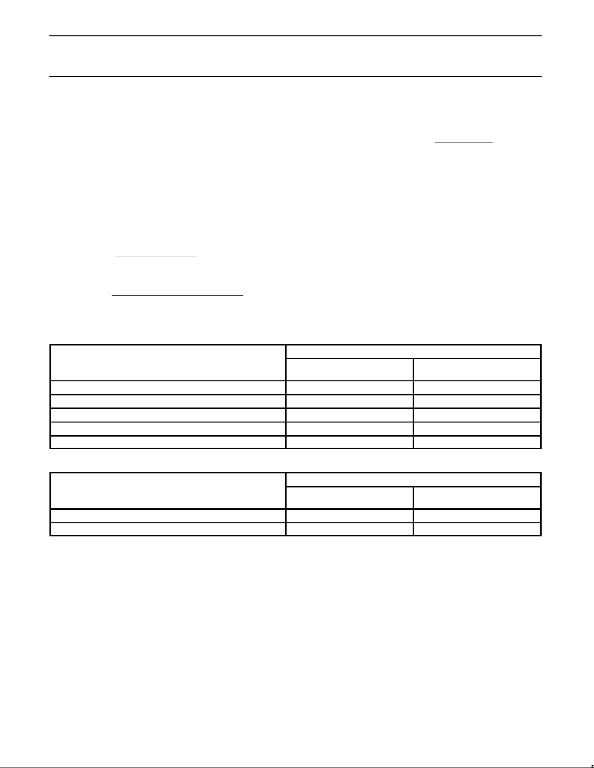
Philips Semiconductors Product specification
80C52/80C54/80C58CMOS single-chip 8-bit microcontrollers
When Timer 2 is in the baud rate generator mode, one should not try
to read or write TH2 and TL2. As a baud rate generator, T imer 2 is
incremented every state time (osc/2) or asynchronously from pin T2;
under these conditions, a read or write of TH2 or TL2 may not be
accurate. The RCAP2 registers may be read, but should not be
written to, because a write might overlap a reload and cause write
and/or reload errors. The timer should be turned off (clear TR2)
before accessing the Timer 2 or RCAP2 registers.
Table 3 shows commonly used baud rates and how they can be
obtained from Timer 2.
Summary Of Baud Rate Equations
Timer 2 is in baud rate generating mode. If Timer 2 is being clocked
through pin T2(P1.0) the baud rate is:
Baud Rate +
If Timer 2 is being clocked internally, the baud rate is:
Baud Rate +
Where f
OSC
Timer 2 Overflow Rate
[32 [65536 * (RCAP2H,RCAP2L)]]
= Oscillator Frequency
16
f
OSC
To obtain the reload value for RCAP2H and RCAP2L, the above
equation can be rewritten as:
f
RCAP2H,RCAP2L + 65536 *
ǒ
32 Baud Rate
Timer/Counter 2 Set-up
Except for the baud rate generator mode, the values given for
T2CON do not include the setting of the TR2 bit. Therefore, bit TR2
must be set, separately, to turn the timer on. see Table 4 for set-up
of Timer 2 as a timer. Also see Table 5 for set-up of Timer 2 as a
counter.
POWER OFF FLAG
The Power Off Flag (POF) is set by on-chip circuitry when the V
level on the 80C54/80C58 rises from 0 to 5V . The POF bit can be
set or cleared by software allowing a user to determine if the reset is
the result of a power-on or a warm start after powerdown. The V
level must remain above 3V for the POF to remain unaffected by the
V
level.
CC
3
Table 4. Timer 2 as a Timer
T2CON
MODE
16-bit Auto-Reload 00H 08H
16-bit Capture 01H 09H
Baud rate generator receive and transmit same baud rate 34H 36H
Receive only 24H 26H
Transmit only 14H 16H
INTERNAL CONTROL
(Note 1)
EXTERNAL CONTROL
OSC
(Note 2)
Ǔ
CC
CC
Table 5. Timer 2 as a Counter
TMOD
MODE
16-bit 02H 0AH
Auto-Reload 03H 0BH
NOTES:
1. Capture/reload occurs only on timer/counter overflow.
2. Capture/reload occurs on timer/counter overflow and a 1-to-0 transition on T2EX (P1.1) pin except when Timer 2 is used in the baud rate
generator mode.
3. POF not present in 80C52.
INTERNAL CONTROL
(Note 1)
EXTERNAL CONTROL
(Note 2)
1996 Aug 16
12
Page 43

Philips Semiconductors Product specification
80C52/80C54/80C58CMOS single-chip 8-bit microcontrollers
OSCILLA T OR CHARACTERISTICS
XTAL1 and XTAL2 are the input and output, respectively , of an
inverting amplifier . The pins can be configured for use as an on-chip
oscillator.
To drive the device from an external clock source, XTAL1 should be
driven while XTAL2 is left unconnected. There are no requirements
on the duty cycle of the external clock signal, because the input to
the internal clock circuitry is through a divide-by-two flip-flop.
However, minimum and maximum high and low times specified in
the data sheet must be observed.
Reset
A reset is accomplished by holding the RST pin high for at least two
machine cycles (24 oscillator periods), while the oscillator is running.
To insure a good power-on reset, the RST pin must be high long
enough to allow the oscillator time to start up (normally a few
milliseconds) plus two machine cycles. At power-on, the voltage on
and RST must come up at the same time for a proper start-up.
V
CC
Ports 1, 2, and 3 will asynchronously be driven to their reset
condition when a voltage above V
(min.) is applied to RESET.
IH1
Idle Mode
In the idle mode (see Table 6), the CPU puts itself to sleep while all
of the on-chip peripherals stay active. The instruction to invoke the
idle mode is the last instruction executed in the normal operating
mode before the idle mode is activated. The CPU contents, the
on-chip RAM, and all of the special function registers remain intact
during this mode. The idle mode can be terminated either by any
enabled interrupt (at which time the process is picked up at the
interrupt service routine and continued), or by a hardware reset
which starts the processor in the same manner as a power-on reset.
Power-Down Mode
To save even more power, a Power Down mode (see Table 6) can
be invoked by software. In this mode, the oscillator is stopped and
the instruction that invoked Power Down is the last instruction
executed. The on-chip RAM and Special Function Registers retain
their values until the Power Down mode is terminated.
On the 80C52/54/58 either a hardware reset or external interrupt
can be used to exit from Power Down. Reset redefines all the SFRs
but does not change the on-chip RAM. An external interrupt allows
both the SFRs and the on-chip RAM to retain their values.
To properly terminate Power Down the reset or external interrupt
should not be executed before V
operating level and must be held active long enough for the
oscillator to restart and stabilize (normally less than 10ms).
With an external interrupt, INT0 and INT1 must be enabled and
configured as level-sensitive. Holding the pin low restarts the
is restored to its normal
CC
oscillator but bringing the pin back high completes the exit. Once the
interrupt is serviced, the next instruction to be executed after RETI
will be the one following the instruction that put the device into
Power Down.
Design Consideration
•When the idle mode is terminated by a hardware reset, the device
normally resumes program execution, from where it left off, up to
two machine cycles before the internal rest algorithm takes
control. On-chip hardware inhibits access to internal RAM in this
event, but access to the port pins is not inhibited. To eliminate the
possibility of an unexpected write when Idle is terminated by reset,
the instruction following the one that invokes Idle should not be
one that writes to a port pin or to external memory.
ONCE Mode
The ONCE (“On-Circuit Emulation”) Mode facilitates testing and
debugging of systems using the 80C52/54/58 without removing the
device from the circuit. The ONCE Mode is invoked by:
1. Pull ALE low while the device is in reset and PSEN
2. Hold ALE low as RST is deactivated.
While the device is in ONCE Mode, the Port 0 pins go into a float
state, and the other port pins and ALE and PSEN
high. The oscillator circuit remains active. While the 80C52/54/58 is
in this mode, an emulator or test CPU can be used to drive the
circuit. Normal operation is restored when a normal reset is applied.
Programmable Clock-Out
The 80C52/54/58 has a new feature. A 50% duty cycle clock can be
programmed to come out on P1.0. This pin, besides being a regular
I/O pin, has two alternate functions. It can be programmed:
1. to input the external clock for Timer/Counter 2, or
2. to output a 50% duty cycle clock ranging from 61Hz to 4MHz at a
16MHz operating frequency.
To configure the Timer/Counter 2 as a clock generator, bit C/T2 (in
T2CON) must be cleared and bit T2OE in T2MOD must be set. Bit
TR2 (T2CON.2) also must be set to start the timer.
The Clock-Out frequency depends on the oscillator frequency and
the reload value of Timer 2 capture registers (RCAP2H, RCAP2L)
as shown in this equation:
Oscillator Frequency
4 (65536 RCAP2H,RCAP2L)
In the Clock-Out mode Timer 2 roll-overs will not generate an
interrupt. This is similar to when it is used as a baud-rate generator.
It is possible to use Timer 2 as a baud-rate generator and a clock
generator simultaneously. Note, however, that the baud-rate and the
Clock-Out frequency will be the same.
is high;
are weakly pulled
Table 6. External Pin Status During Idle and Power-Down Mode
MODE
Idle Internal 1 1 Data Data Data Data
Idle External 1 1 Float Data Address Data
Power-down Internal 0 0 Data Data Data Data
Power-down External 0 0 Float Data Data Data
1996 Aug 16
PROGRAM
MEMORY
ALE PSEN PORT 0 PORT 1 PORT 2 PORT 3
13
Page 44

Philips Semiconductors Product specification
80C52/80C54/80C58CMOS single-chip 8-bit microcontrollers
Enhanced UART
The UART operates in all of the usual modes that are described in
the first section of
Microcontrollers
detect by looking for missing stop bits, and automatic address
recognition. The 80C52/54/58 UART also fully supports
multiprocessor communication as does the standard 80C51 UART.
When used for framing error detect the UART looks for missing stop
bits in the communication. A missing bit will set the FE bit in the
SCON register. The FE bit shares the SCON.7 bit with SM0 and the
function of SCON.7 is determined by PCON.6 (SMOD0) (see
Figure 7). If SMOD0 is set then SCON.7 functions as FE. SCON.7
functions as SM0 when SMOD0 is cleared. When used as FE
SCON.7 can only be cleared by software. Refer to Figure 8.
Automatic Address Recognition
Automatic Address Recognition is a feature which allows the UART
to recognize certain addresses in the serial bit stream by using
hardware to make the comparisons. This feature saves a great deal
of software overhead by eliminating the need for the software to
examine every serial address which passes by the serial port. This
feature is enabled by setting the SM2 bit in SCON. In the 9 bit UART
modes, mode 2 and mode 3, the Receive Interrupt flag (RI) will be
automatically set when the received byte contains either the “Given”
address or the “Broadcast” address. The 9 bit mode requires that
the 9th information bit is a 1 to indicate that the received information
is an address and not data. Automatic address recognition is shown
in Figure 9.
The 8 bit mode is called Mode 1. In this mode the RI flag will be set
if SM2 is enabled and the information received has a valid stop bit
following the 8 address bits and the information is either a Given or
Broadcast address.
Mode 0 is the Shift Register mode and SM2 is ignored.
Using the Automatic Address Recognition feature allows a master to
selectively communicate with one or more slaves by invoking the
Given slave address or addresses. All of the slaves may be
contacted by using the Broadcast address. Two special Function
Registers are used to define the slave’s address, SADDR, and the
address mask, SADEN. SADEN is used to define which bits in the
SADDR are to b used and which bits are “don’t care”. The SADEN
mask can be logically ANDed with the SADDR to create the “|Given”
address which the master will use for addressing each of the slaves.
Use of the Given address allows multiple slaves to be recognized
while excluding others. The following examples will help to show the
versatility of this scheme:
Slave 0 SADDR = 1100 0000
Data Handbook IC20, 80C51-Based 8-Bit
. In addition the UART can perform framing error
SADEN = 1111 1101
Given = 1100 00X0
Slave 1 SADDR = 1100 0000
SADEN = 1111 1110
Given = 1100 000X
In the above example SADDR is the same and the SADEN data is
used to differentiate between the two slaves. Slave 0 requires a 0 in
bit 0 and it ignores bit 1. Slave 1 requires a 0 in bit 1 and bit 0 is
ignored. A unique address for Slave 0 would be 1100 0010 since
slave 1 requires a 0 in bit 1. A unique address for slave 1 would be
1100 0001 since a 1 in bit 0 will exclude slave 0. Both slaves can be
selected at the same time by an address which has bit 0 = 0 (for
slave 0) and bit 1 = 0 (for slave 1). Thus, both could be addressed
with 1100 0000.
In a more complex system the following could be used to select
slaves 1 and 2 while excluding slave 0:
Slave 0 SADDR = 1100 0000
SADEN = 1111 1001
Given = 1100 0XX0
Slave 1 SADDR = 1110 0000
SADEN = 1111 1010
Given = 11 10 0X0X
Slave 2 SADDR = 1110 0000
SADEN = 1111 1100
Given = 1110 00XX
In the above example the differentiation among the 3 slaves is in the
lower 3 address bits. Slave 0 requires that bit 0 = 0 and it can be
uniquely addressed by 1110 01 10. Slave 1 requires that bit 1 = 0 and
it can be uniquely addressed by 1110 and 0101. Slave 2 requires
that bit 2 = 0 and its unique address is 1110 0011. To select Slaves 0
and 1 and exclude Slave 2 use address 1110 0100, since it is
necessary t make bit 2 = 1 to exclude slave 2.
The Broadcast Address for each slave is created by taking the
logical OR of SADDR and SADEN. Zeros in this result are teated as
don’t-cares. In most cases, interpreting the don’t-cares as ones, the
broadcast address will be FF hexadecimal.
Upon reset SADDR (SFR address 0A9H) and SADEN (SFR
address 0B9H) are leaded with 0s. This produces a given address
of all “don’t cares” as well as a Broadcast address of all “don’t
cares”. this effectively disables the Automatic Addressing mode and
allows the microcontroller to use standard 80C51 type UART drivers
which do not make use of this feature.
1996 Aug 16
14
Page 45
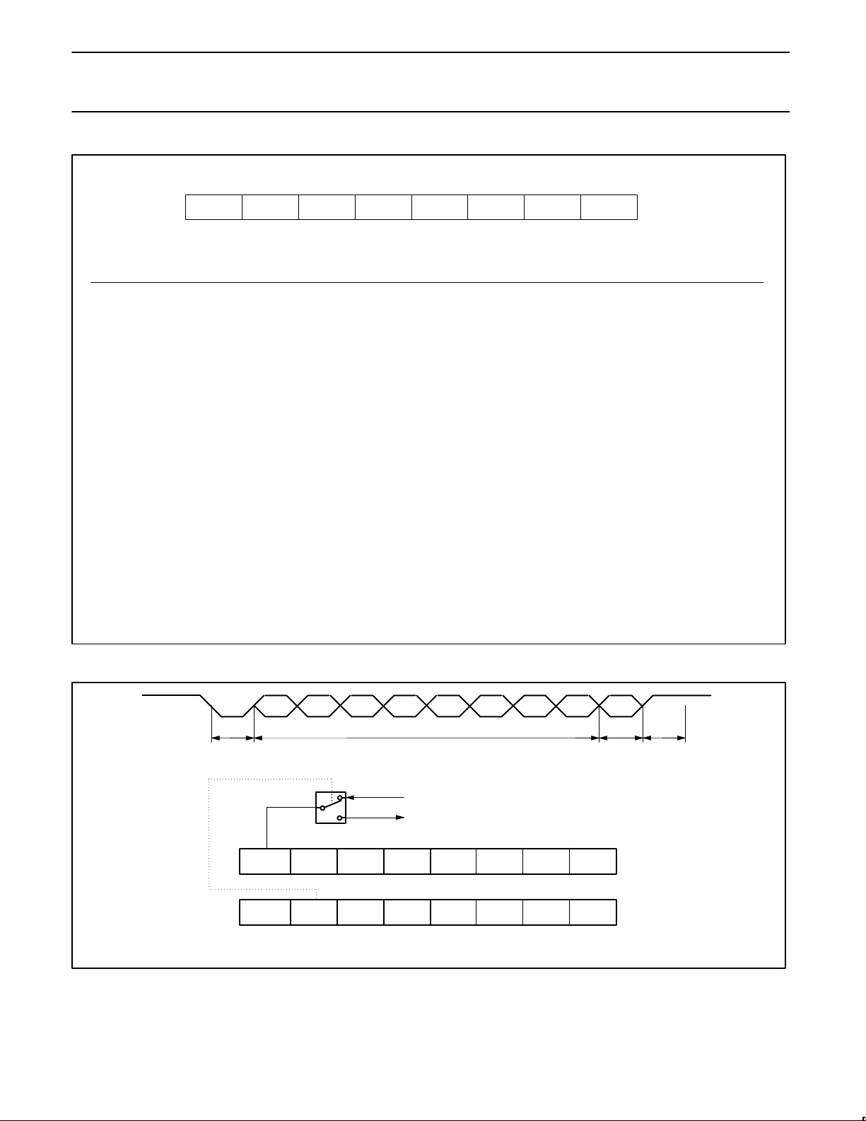
Philips Semiconductors Product specification
80C52/80C54/80C58CMOS single-chip 8-bit microcontrollers
SCON Address = 98H
Reset Value = 0000 0000B
Bit Addressable
SM0/FE SM1 SM2 REN TB8 RB8 Tl Rl
Bit: 76543210
(SMOD0 = 0/1)*
Symbol Function
FE Framing Error bit. This bit is set by the receiver when an invalid stop bit is detected. The FE bit is not cleared by valid
frames but should be cleared by software. The SMOD0 bit must be set to enable access to the FE bit.
SM0 Serial Port Mode Bit 0, (SMOD0 must = 0 to access bit SM0)
SM1 Serial Port Mode Bit 1
SM0 SM1 Mode Description Baud Rate**
0 0 0 shift register f
OSC
/12
0 1 1 8-bit UART variable
1 0 2 9-bit UART f
OSC
/64 or f
OSC
/32
1 1 3 9-bit UART variable
SM2 Enables the Automatic Address Recognition feature in Modes 2 or 3. If SM2 = 1 then Rl will not be set unless the
received 9th data bit (RB8) is 1, indicating an address, and the received byte is a Given or Broadcast Address.
In Mode 1, if SM2 = 1 then Rl will not be activated unless a valid stop bit was received, and the received byte is a
Given or Broadcast Address. In Mode 0, SM2 should be 0.
REN Enables serial reception. Set by software to enable reception. Clear by software to disable reception.
TB8 The 9th data bit that will be transmitted in Modes 2 and 3. Set or clear by software as desired.
RB8 In modes 2 and 3, the 9th data bit that was received. In Mode 1, if SM2 = 0, RB8 is the stop bit that was received.
In Mode 0, RB8 is not used.
Tl Transmit interrupt flag. Set by hardware at the end of the 8th bit time in Mode 0, or at the beginning of the stop bit in the
other modes, in any serial transmission. Must be cleared by software.
Rl Receive interrupt flag. Set by hardware at the end of the 8th bit time in Mode 0, or halfway through the stop bit time in
the other modes, in any serial reception (except see SM2). Must be cleared by software.
NOTE:
*SMOD0 is located at PCON6.
**f
= oscillator frequency
OSC
Figure 7. SCON: Serial Port Control Register
SU00043
1996 Aug 16
D0 D1 D2 D3 D4 D5 D6 D7 D8
START
BIT
SM0 / FE SM1 SM2 REN TB8 RB8 TI RI
SMOD1 SMOD0 – POF GF1 GF0 PD IDL
0 : SCON.7 = SM0
1 : SCON.7 = FE
DATA BYTE
SET FE BIT IF STOP BIT IS 0 (FRAMING ERROR)
SM0 TO UART MODE CONTROL
Figure 8. UART Framing Error Detection
15
ONLY IN
MODE 2, 3
SCON
(98H)
PCON
(87H)
STOP
BIT
SU00747
Page 46
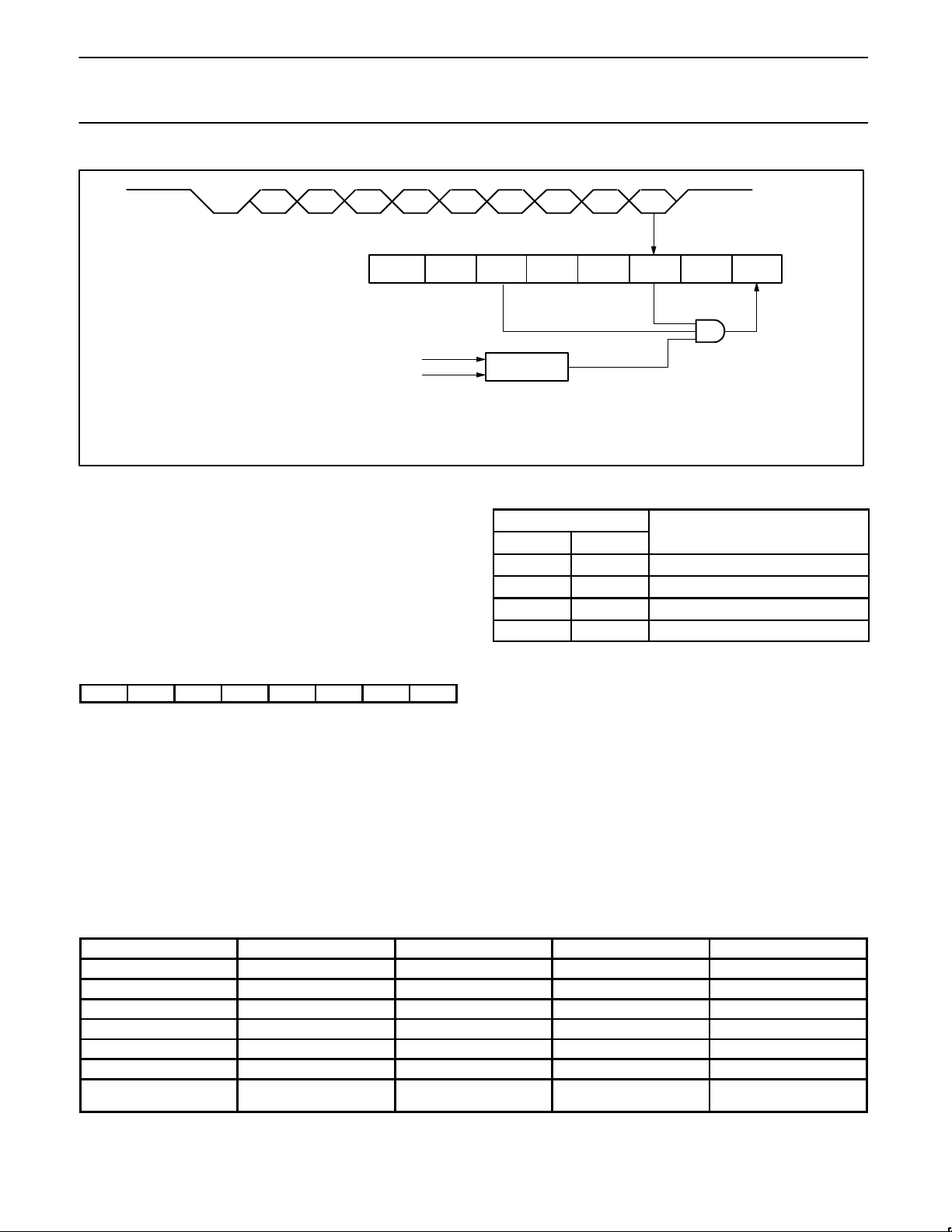
Philips Semiconductors Product specification
INTERRUPT PRIORITY LEVEL
80C52/80C54/80C58CMOS single-chip 8-bit microcontrollers
D0 D1 D2 D3 D4 D5 D6 D7 D8
SM0 SM1 SM2 REN TB8 RB8 TI RI
1
1
RECEIVED ADDRESS D0 TO D7
PROGRAMMED ADDRESS
IN UART MODE 2 OR MODE 3 AND SM2 = 1:
INTERRUPT IF REN=1, RB8=1 AND “RECEIVED ADDRESS” = “PROGRAMMED ADDRESS”
– WHEN OWN ADDRESS RECEIVED, CLEAR SM2 TO RECEIVE DATA BYTES
– WHEN ALL DATA BYTES HAVE BEEN RECEIVED: SET SM2 TO WAIT FOR NEXT ADDRESS.
Figure 9. UART Multiprocessor Communication, Automatic Address Recognition
Interrupt Priority Structure
The 80C52/54/58 has a 6-source four-level interrupt structure. There
are 3 SFRs associated with the interrupts on the 80C52/54/58. They
are the IE and IP. (See Figures 10 and 11.) In addition, there is the
IPH (Interrupt Priority High) register that makes the four-level
interrupt structure possible. The IPH is located at SFR address B7H.
The structure of the IPH register and a description of its bits is
shown below:
IPH (Interrupt Priority High) (B7H)
76543210
––PT2H PSH PT1H PX1H PT0H PX0H
IPH.0 PX0H External interrupt 0 priority high
IPH.1 PT0H Timer 0 interrupt priority high
IPH.2 PX1H External interrupt 1 priority high
IPH.3 PT1H Timer 1 interrupt priority high
IPH.4 PSH Serial Port interrupt high
IPH.5 PT2H Timer 2 interrupt priority high
IPH.6 — Not implemented
IPH.7 — Not implemented
The function of the IPH SFR is simple and when combined with the
IP SFR determines the priority of each interrupt. The priority of each
interrupt is determined as shown in the following table:
1
0
11 X
COMPARATOR
PRIORITY BITS
IPH.x IP.x
0 0 Level 0 (lowest priority)
0 1 Level 1
1 0 Level 2
1 1 Level 3 (highest priority)
The priority scheme for servicing the interrupts is the same as that
for the 80C51, except there are four interrupt levels on the
80C52/54/58 rather than two as on the 80C51. An interrupt will be
serviced as long as an interrupt of equal or higher priority is not
already being serviced. If an interrupt of equal or higher level priority
is being serviced, the new interrupt will wait until it is finished before
being serviced. If a lower priority level interrupt is being serviced, it
will be stopped and the new interrupt serviced. When the new
interrupt is finished, the lower priority level interrupt that was
stopped will be completed.
SCON
(98H)
SU00045
Table 7. Interrupt Table
SOURCE POLLING PRIORITY REQUEST BITS HARDWARE CLEAR? VECTOR ADDRESS
X0 1 IE0 N (L)1Y (T)
T0 2 TP0 Y 0BH
X1 3 IE1 N (L) Y (T) 13H
T1 4 TF1 Y 1BH
SP 5 R1, TI N 23H
T2 6 TF2, EXF2 N 2BH
PCA 7 CF, CCFn
NOTES:
1. L = Level activated
2. T = Transition activated
1996 Aug 16
n = 0–4
16
2
03H
N 33H
Page 47
Philips Semiconductors Product specification
80C52/80C54/80C58CMOS single-chip 8-bit microcontrollers
01234567
ET0EX1ET1ESET2—EA
Enable Bit = 1 enables the interrupt.
Enable Bit = 0 disables it.
BIT SYMBOL FUNCTION
IE.7 EA Global disable bit. If EA = 0, all interrupts are disabled. If EA = 1, each interrupt can be individually
enabled or disabled by setting or clearing its enable bit.
IE.6 —
IE.5 ET2 Timer 2 interrupt enable bit.
IE.4 ES Serial Port interrupt enable bit.
IE.3 ET1 Timer 1 interrupt enable bit.
IE.2 EX1 External interrupt 1 enable bit.
IE.1 ET0 Timer 0 interrupt enable bit.
IE.0 EX0 External interrupt 0 enable bit.
Figure 10. IE Registers
EX0IE0 (A8H)
SU00743
Priority Bit = 1 assigns high priority
Priority Bit = 0 assigns low priority
BIT SYMBOL FUNCTION
IP.7 — Not implemented, reserved for future use.
IP.6 —
IP.5 PT2 Timer 2 interrupt priority bit.
IP.4 PS Serial Port interrupt priority bit.
IP.3 PT1 Timer 1 interrupt priority bit.
IP.2 PX1 External interrupt 1 priority bit.
IP.1 PT0 Timer 0 interrupt priority bit.
IP.0 PX0 External interrupt 0 priority bit.
Figure 11. IP Registers
01234567
PT0PX1PT1PSPT2——
PX0IP0 (B8H)
SU00744
1996 Aug 16
17
Page 48
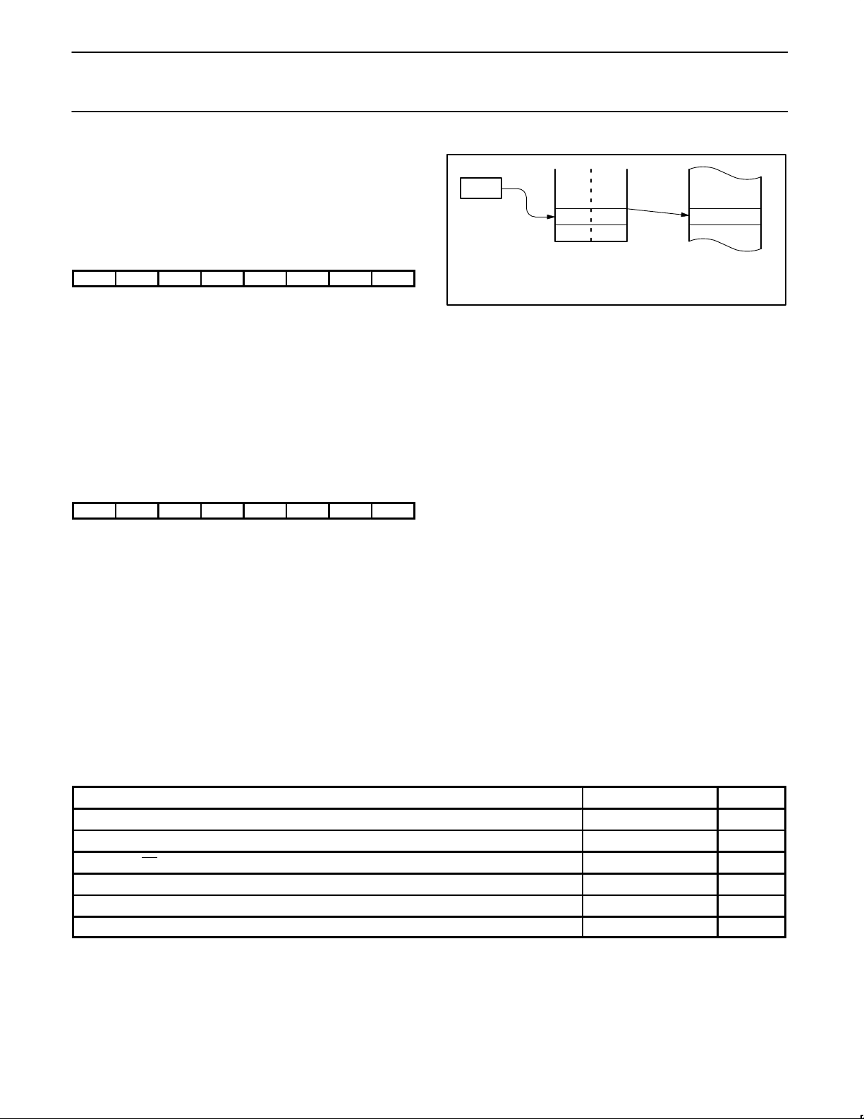
Philips Semiconductors Product specification
80C52/80C54/80C58CMOS single-chip 8-bit microcontrollers
Reduced EMI Mode
The AO bit (AUXR.0) in the AUXR register when set disables the
ALE output.
80C52/80C54/80C58 Reduced EMI Mode
AUXR (8EH)
76543210
–––––––AO
AO: Turns off ALE output.
Dual Data Pointer Register (DPTR)
The dual DPTR structure (see Figure 12) is a way by which the
80C52/54/58 will specify the address of an external data memory
location. There are two 16-bit DPTR registers that address the
external memory , and a single bit called DPS = AUXR1/bit0 that
allows the program code to switch between them.
•Register Name: AUXR1#
•SFR Address: A2H
•Reset Value: xxxxxxx0B
76543210
–––––––DPS
Where:
DPS = AUXR1/bit0 = Switches between DPTR0 and DPTR1.
Select Reg DPS
DPTR0 0
DPTR1 1
The DPS bit status whould be saved by software when switching
between DPTR0 and DPTR1.
DPS
BIT0
AUXR1
DPH
(83H)
DPL
(82H)
DPTR1
DPTR0
EXTERNAL
DATA
MEMORY
SU00745A
Figure 12. DPTR Structure
DPTR Instructions
The instructions that refer to DPTR refer to the data pointer that is
currently selected using the AUXR1/bit 0 register. The six
instructions that use the DPTR are as follows:
INC DPTR Increments the data pointer by 1
MOV DPTR, #data16 Loads the DPTR with a 16-bit constant
MOV A, @ A+DPTR Move code byte relative to DPTR to
ACC
MOVX A, @ DPTR Move external RAM (16-bit address) to
ACC
MOVX @ DPTR , A Move ACC to external RAM (16-bit
address)
JMP @ A + DPTR Jump indirect relative to DPTR
The data pointer can be accessed on a byte-by-byte basis by
specifying the Low or High byte in an instruction which accesses the
SFRs. See application note AN458 for detailed operation
ABSOLUTE MAXIMUM RATINGS
Operating temperature under bias 0 to +70 or –40 to +85 °C
Storage temperature range –65 to +150 °C
Voltage on EA/VPP pin to V
Voltage on any other pin to V
Maximum IOL per I/O pin 15 mA
Power dissipation (based on package heat transfer limitations, not device power consumption) 1.5 W
NOTES:
1. Stresses above those listed under Absolute Maximum Ratings may cause permanent damage to the device. This is a stress rating only and
functional operation of the device at these or any conditions other than those described in the AC and DC Electrical Characteristics section
of this specification is not implied.
2. This product includes circuitry specifically designed for the protection of its internal devices from the damaging effects of excessive static
charge. Nonetheless, it is suggested that conventional precautions be taken to avoid applying greater than the rated maxima.
3. Parameters are valid over operating temperature range unless otherwise specified. All voltages are with respect to V
noted.
1996 Aug 16
SS
SS
1, 2, 3
PARAMETER
18
RATING UNIT
0 to +13.0 V
–0.5 to +6.5 V
unless otherwise
SS
Page 49
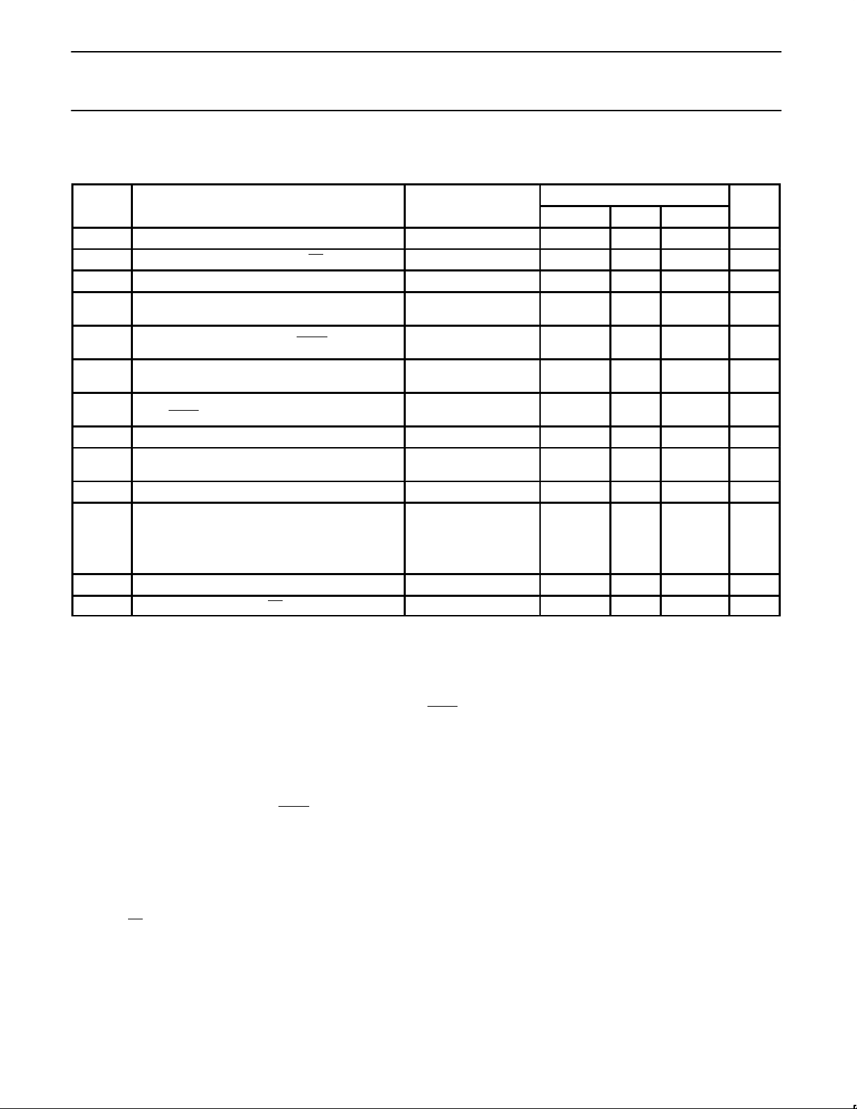
Philips Semiconductors Product specification
SYMBOL
PARAMETER
TEST
UNIT
80C52/80C54/80C58CMOS single-chip 8-bit microcontrollers
DC ELECTRICAL CHARACTERISTICS
T
= 0°C to +70°C or –40°C to +85°C, VCC = 5.0V ±10%; VSS = 0V
amb
CC
LIMITS
3
1
MAX
VCC+0.5 V
0.4 V
0.4 V
–650 µA
16
50
75
4
mA
µA
µA
mA
TEST
V
V
V
V
V
V
V
I
I
I
I
R
C
IL
IH
IH1
OL
OL1
OH
OH1
IL
TL
LI
CC
RST
IO
CONDITIONS
Input low voltage 4.5V < VCC < 5.5V –0.5 0.2VCC–0.1 V
Input high voltage (ports 0, 1, 2, 3, EA) 0.2VCC+0.9 VCC+0.5 V
Input high voltage, XTAL1, RST 0.7V
Output low voltage, ports 1, 2, 3
Output low voltage, port 0, ALE, PSEN
Output high voltage, ports 1, 2, 3
Output high voltage (port 0 in external bus mode),
ALE
9
, PSEN
3
8
8, 7
3
VCC = 4.5V
= 1.6mA
I
OL
VCC = 4.5V
= 3.2mA
I
OL
VCC = 4.5V
= –30µA
I
OH
VCC = 4.5V
= –3.2mA
I
OH
2
2
Logical 0 input current, ports 1, 2, 3 VIN = 0.4V –1 –50 µA
Logical 1-to-0 transition current, ports 1, 2, 3
6
VIN = 2.0V
See note 4
Input leakage current, port 0 0.45 < VIN < VCC – 0.3 ±10 µA
Power supply current (see Figure 20):
Active mode @ 16MHz
Idle mode @ 16MHz
5
5
Power-down mode
See note 5
= 0 to +70°C
T
amb
= –40 to +85°C
T
amb
Internal reset pull-down resistor 40 225 kΩ
Pin capacitance10 (except EA) 15 pF
MIN TYP
VCC – 0.7 V
VCC – 0.7 V
NOTES:
1. Typical ratings are not guaranteed. The values listed are at room temperature, 5V.
2. Capacitive loading on ports 0 and 2 may cause spurious noise to be superimposed on the V
to external bus capacitance discharging into the port 0 and port 2 pins when these pins make 1-to-0 transitions during bus operations. In the
s of ALE and ports 1 and 3. The noise is due
OL
worst cases (capacitive loading > 100pF), the noise pulse on the ALE pin may exceed 0.8V . In such cases, it may be desirable to qualify
ALE with a Schmitt Trigger, or use an address latch with a Schmitt Trigger STROBE input. I
single output sinks more than 5mA and no more than two outputs exceed the test conditions.
3. Capacitive loading on ports 0 and 2 may cause the V
address bits are stabilizing.
on ALE and PSEN to momentarily fall below the (VCC–0.7) specification when the
OH
can exceed these conditions provided that no
OL
4. Pins of ports 1, 2 and 3 source a transition current when they are being externally driven from 1 to 0. The transition current reaches its
maximum value when V
5. See Figures 21 through 24 for I
Active Mode: I
Idle Mode: I
6. This value applies to T
7. Load capacitance for port 0, ALE, and PSEN
8. Under steady state (non-transient) conditions, I
Maximum I
Maximum I
Maximum total I
exceeds the test condition, VOL may exceed the related specification. Pins are not guaranteed to sink current greater than the listed
If I
OL
test conditions.
per port pin: 15mA (*NOTE: This is 85°C specification.)
OL
per 8-bit port: 26mA
OL
9. ALE is tested to V
10.Pin capacitance is characterized but not tested. Pin capacitance is less than 25pF. Pin capacitance of ceramic package is less than 15pF
(except EA
it is 25pF).
is approximately 2V .
IN
= 0.9 × FREQ + 1.1;
CC
= 0.18 × FREQ +1.0; See Figure 20.
CC
amb
for all outputs: 71mA
OL
, except when ALE is off then VOH is the voltage specification.
OH1
test conditions.
CC
= 0°C to +70°C. For T
= 100pF, load capacitance for all other outputs = 80pF .
= –40°C to +85°C, ITL = –750µA.
amb
must be externally limited as follows:
OL
1996 Aug 16
19
Page 50
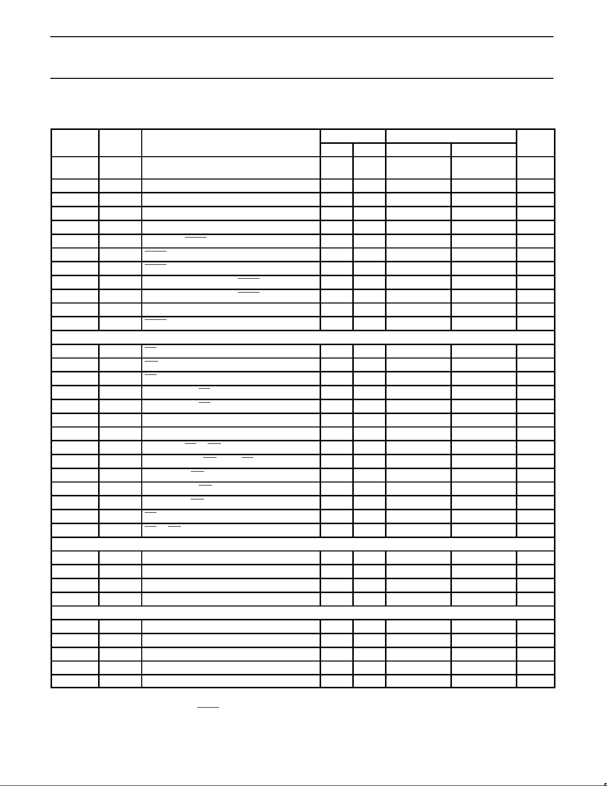
Philips Semiconductors Product specification
80C52/80C54/80C58CMOS single-chip 8-bit microcontrollers
AC ELECTRICAL CHARACTERISTICS
T
= 0°C to +70°C or –40°C to +85°C, VCC = 5V ±10%, VSS = 0V
amb
1, 2, 3
16MHz CLOCK VARIABLE CLOCK
SYMBOL FIGURE PARAMETER MIN MAX MIN MAX UNIT
1/t
t
LHLL
t
AVLL
t
LLAX
t
LLIV
t
LLPL
t
PLPH
t
PLIV
t
PXIX
t
PXIZ
t
AVIV
t
PLAZ
CLCL
13 Oscillator frequency
Speed versions : E
13 ALE pulse width 85 2t
13 Address valid to ALE low 22 t
13 Address hold after ALE low 32 t
13 ALE low to valid instruction in 150 4t
13 ALE low to PSEN low 32 t
13 PSEN pulse width 142 3t
13 PSEN low to valid instruction in
4
82 3t
3.5 16 MHz
–40 ns
CLCL
–40 ns
CLCL
–30 ns
CLCL
–100 ns
CLCL
–30 ns
CLCL
–45 ns
CLCL
–105 ns
CLCL
13 Input instruction hold after PSEN 0 0 ns
13 Input instruction float after PSEN 37 t
13 Address to valid instruction in
4
207 5t
–25 ns
CLCL
–105 ns
CLCL
13 PSEN low to address float 10 10 ns
Data Memory
t
RLRH
t
WLWH
t
RLDV
t
RHDX
t
RHDZ
t
LLDV
t
AVDV
t
LLWL
t
AVWL
t
QVWX
t
WHQX
t
QVWH
t
RLAZ
t
WHLH
14, 15 RD pulse width 275 6t
14, 15 WR pulse width 275 6t
14, 15 RD low to valid data in 147 5t
–100 ns
CLCL
–100 ns
CLCL
–165 ns
CLCL
14, 15 Data hold after RD 0 0 ns
14, 15 Data float after RD 65 2t
14, 15 ALE low to valid data in 350 8t
14, 15 Address to valid data in 397 9t
14, 15 ALE low to RD or WR low 137 239 3t
14, 15 Address valid to WR low or RD low 122 4t
14, 15 Data valid to WR transition 13 t
14, 15 Data hold after WR 13 t
15 Data valid to WR high 287 7t
–50 3t
CLCL
–130 ns
CLCL
–50 ns
CLCL
–50 ns
CLCL
–150 ns
CLCL
–60 ns
CLCL
–150 ns
CLCL
–165 ns
CLCL
+50 ns
CLCL
14, 15 RD low to address float 0 0 ns
14, 15 RD or WR high to ALE high 23 103 t
–40 t
CLCL
+40 ns
CLCL
External Clock
t
CHCX
t
CLCX
t
CLCH
t
CHCL
17 High time 20 20 t
17 Low time 20 20 t
CLCL–tCLCX
CLCL–tCHCX
ns
ns
17 Rise time 20 20 ns
17 Fall time 20 20 ns
Shift Register
t
XLXL
t
QVXH
t
XHQX
t
XHDX
t
XHDV
16 Serial port clock cycle time 750 12t
16 Output data setup to clock rising edge 492 10t
16 Output data hold after clock rising edge 8 2t
CLCL
CLCL
CLCL
–133 ns
–117 ns
ns
16 Input data hold after clock rising edge 0 0 ns
16 Clock rising edge to input data valid 492 10t
–133 ns
CLCL
NOTES:
1. Parameters are valid over operating temperature range unless otherwise specified.
2. Load capacitance for port 0, ALE, and PSEN
= 100pF, load capacitance for all other outputs = 80pF .
3. Interfacing the 80C52/54/58 to devices with float times up to 45ns is permitted. This limited bus contention will not cause damage to Port 0
drivers.
4. See application note AN457 for external memory interfacing.
1996 Aug 16
20
Page 51
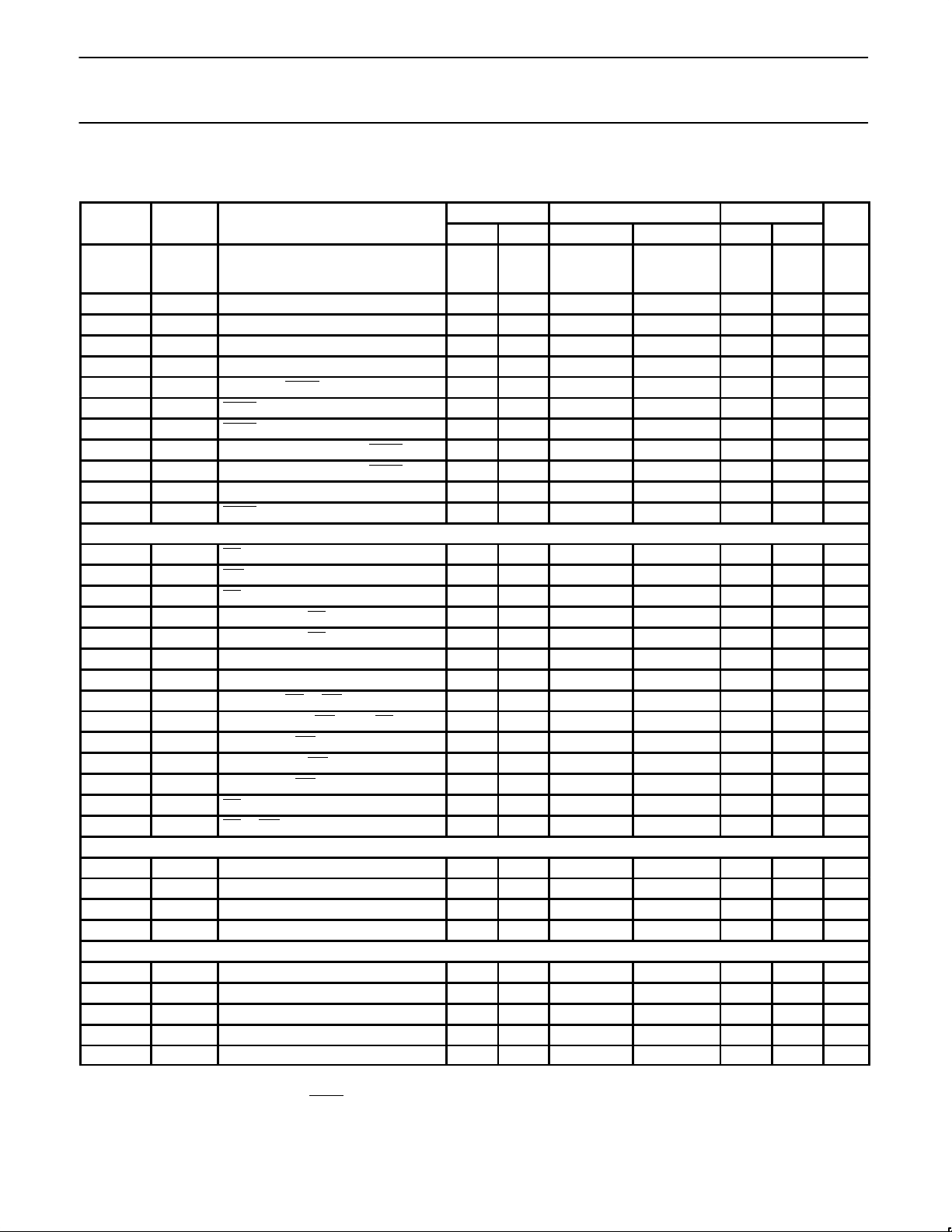
Philips Semiconductors Product specification
80C52/80C54/80C58CMOS single-chip 8-bit microcontrollers
AC ELECTRICAL CHARACTERISTICS
T
= 0°C to +70°C or –40°C to +85°C, VCC = 5V ±10%, VSS = 0V
amb
1, 2, 3
24MHz CLOCK VARIABLE CLOCK
4
33MHz CLOCK
SYMBOL FIGURE PARAMETER MIN MAX MIN MAX MIN MAX UNIT
1/t
t
LHLL
t
AVLL
t
LLAX
t
LLIV
t
LLPL
t
PLPH
t
PLIV
t
PXIX
t
PXIZ
t
AVIV
t
PLAZ
CLCL
13 Oscillator frequency
Speed versions : I (24MHz)
3.5 24
: N (33MHz)
13 ALE pulse width 43 2t
13 Address valid to ALE low 17 t
13 Address hold after ALE low 17 t
13 ALE low to valid instruction in 102 4t
13 ALE low to PSEN low 17 t
13 PSEN pulse width 80 3t
13 PSEN low to valid instruction in 65 3t
3.5 33
3.5 33
–40 21 ns
CLCL
–25 5 ns
CLCL
–25 ns
CLCL
–65 55 ns
CLCL
–25 5 ns
CLCL
–45 45 ns
CLCL
–60 30 ns
CLCL
MHz
13 Input instruction hold after PSEN 0 0 0 ns
13 Input instruction float after PSEN 17 t
13 Address to valid instruction in 128 5t
–25 5 ns
CLCL
–80 70 ns
CLCL
13 PSEN low to address float 10 10 10 ns
Data Memory
t
RLRH
t
WLWH
t
RLDV
t
RHDX
t
RHDZ
t
LLDV
t
AVDV
t
LLWL
t
AVWL
t
QVWX
t
WHQX
t
QVWH
t
RLAZ
t
WHLH
14, 15 RD pulse width 150 6t
14, 15 WR pulse width 150 6t
14, 15 RD low to valid data in 118 5t
–100 82 ns
CLCL
–100 82 ns
CLCL
–90 60 ns
CLCL
14, 15 Data hold after RD 0 0 0 ns
14, 15 Data float after RD 55 2t
14, 15 ALE low to valid data in 183 8t
14, 15 Address to valid data in 210 9t
14, 15 ALE low to RD or WR low 75 175 3t
14, 15 Address valid to WR low or RD low 92 4t
14, 15 Data valid to WR transition 12 t
14, 15 Data hold after WR 17 t
15 Data valid to WR high 162 7t
–50 3t
CLCL
–75 45 ns
CLCL
–30 0 ns
CLCL
–25 5 ns
CLCL
–130 80 ns
CLCL
–28 32 ns
CLCL
–150 90 ns
CLCL
–165 105 ns
CLCL
+50 40 140 ns
CLCL
14, 15 RD low to address float 0 0 0 ns
14, 15 RD or WR high to ALE high 17 67 t
CLCL
–25 t
+25 5 55 ns
CLCL
External Clock
t
CHCX
t
CLCX
t
CLCH
t
CHCL
17 High time 17 17 t
17 Low time 17 17 t
CLCL–tCLCX
CLCL–tCHCX
17 Rise time 5 5 ns
17 Fall time 5 5 ns
ns
ns
Shift Register
t
XLXL
t
QVXH
t
XHQX
t
XHDX
t
XHDV
16 Serial port clock cycle time 505 12t
16 Output data setup to clock rising edge 283 10t
16 Output data hold after clock rising edge 3 2t
CLCL
CLCL
CLCL
–133 167 ns
–80 ns
360 ns
16 Input data hold after clock rising edge 0 0 0 ns
16 Clock rising edge to input data valid 283 10t
–133 167 ns
CLCL
NOTES:
1. Parameters are valid over operating temperature range unless otherwise specified.
2. Load capacitance for port 0, ALE, and PSEN
= 100pF, load capacitance for all other outputs = 80pF .
3. Interfacing the 80C52/54/58 to devices with float times up to 45ns is permitted. This limited bus contention will not cause damage to Port 0
drivers.
4. Variable clock is specified for oscillator frequencies greater than 16MHz to 33MHz. For frequencies equal or less than 16MHz, see 16MHz
“AC Electrial Characteristics”, page 20.
1996 Aug 16
21
Page 52
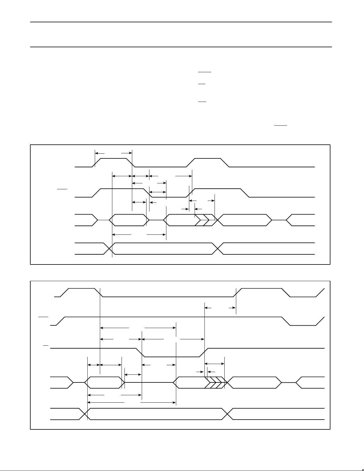
Philips Semiconductors Product specification
80C52/80C54/80C58CMOS single-chip 8-bit microcontrollers
EXPLANATION OF THE AC SYMBOLS
Each timing symbol has five characters. The first character is always
‘t’ (= time). The other characters, depending on their positions,
indicate the name of a signal or the logical status of that signal. The
designations are:
A – Address
C – Clock
D – Input data
H – Logic level high
I – Instruction (program memory contents)
L – Logic level low, or ALE
t
ALE
LHLL
P – PSEN
Q – Output data
R–RD
signal
t – Time
V – Valid
W– WR
signal
X – No longer a valid logic level
Z – Float
Examples: t
= Time for address valid to ALE low.
AVLL
t
=Time for ALE low to PSEN low.
LLPL
ALE
PSEN
RD
PSEN
PORT 0
PORT 2
t
t
AVLL
LLPL
t
LLAX
A0–A7 A0–A7
t
AVIV
t
PLPH
t
LLIV
t
PLIV
t
t
PLAZ
t
PXIX
INSTR IN
A0–A15 A8–A15
PXIZ
Figure 13. External Program Memory Read Cycle
t
WHLH
t
LLDV
t
LLWL
t
RLRH
SU00006
t
AVLL
PORT 0
PORT 2
1996 Aug 16
t
LLAX
A0–A7
FROM RI OR DPL
t
AVWL
t
t
t
RLAZ
t
AVDV
P2.0–P2.7 OR A8–A15 FROM DPF A0–A15 FROM PCH
RLDV
t
RHDX
DATA IN A0–A7 FROM PCL INSTR IN
RHDZ
Figure 14. External Data Memory Read Cycle
22
SU00025
Page 53
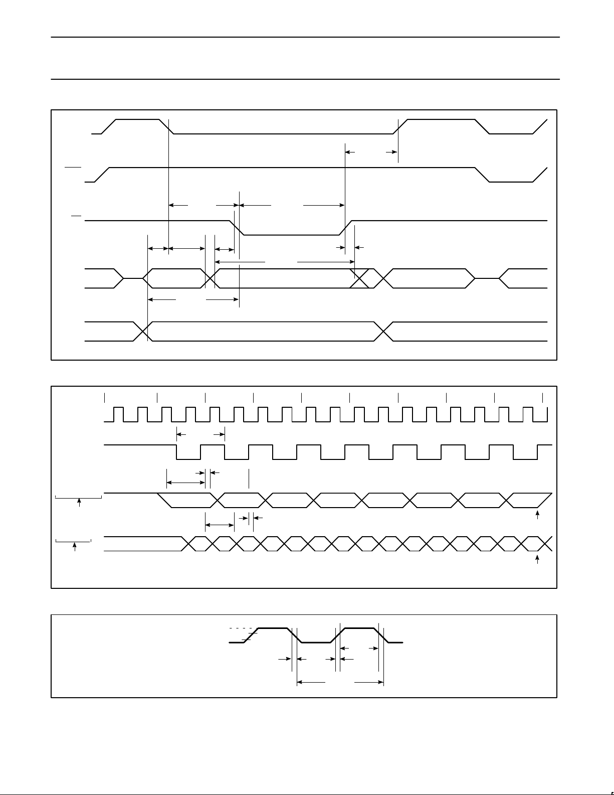
Philips Semiconductors Product specification
80C52/80C54/80C58CMOS single-chip 8-bit microcontrollers
ALE
t
WHLH
PSEN
WR
PORT 0
PORT 2
INSTRUCTION
ALE
CLOCK
OUTPUT DATA
WRITE TO SBUF
INPUT DATA
CLEAR RI
t
WLWH
t
WHQX
t
QVWH
DATA OUT A0–A7 FROM PCL INSTR IN
SU00026
t
AVLL
t
t
LLAX
A0–A7
FROM RI OR DPL
t
AVWL
LLWL
t
QVWX
P2.0–P2.7 OR A8–A15 FROM DPF A0–A15 FROM PCH
Figure 15. External Data Memory Write Cycle
012345678
t
XLXL
t
t
QVXH
t
XHDV
VALID VALID VALID VALID VALID VALID VALID VALID
XHQX
1230 4567
t
XHDX
SET TI
SET RI
SU00027
Figure 16. Shift Register Mode Timing
1996 Aug 16
VCC–0.5
0.45V
0.7V
CC
0.2VCC–0.1
t
CHCL
t
CLCX
t
CLCL
t
CHCX
t
CLCH
Figure 17. External Clock Drive
23
SU00009
Page 54
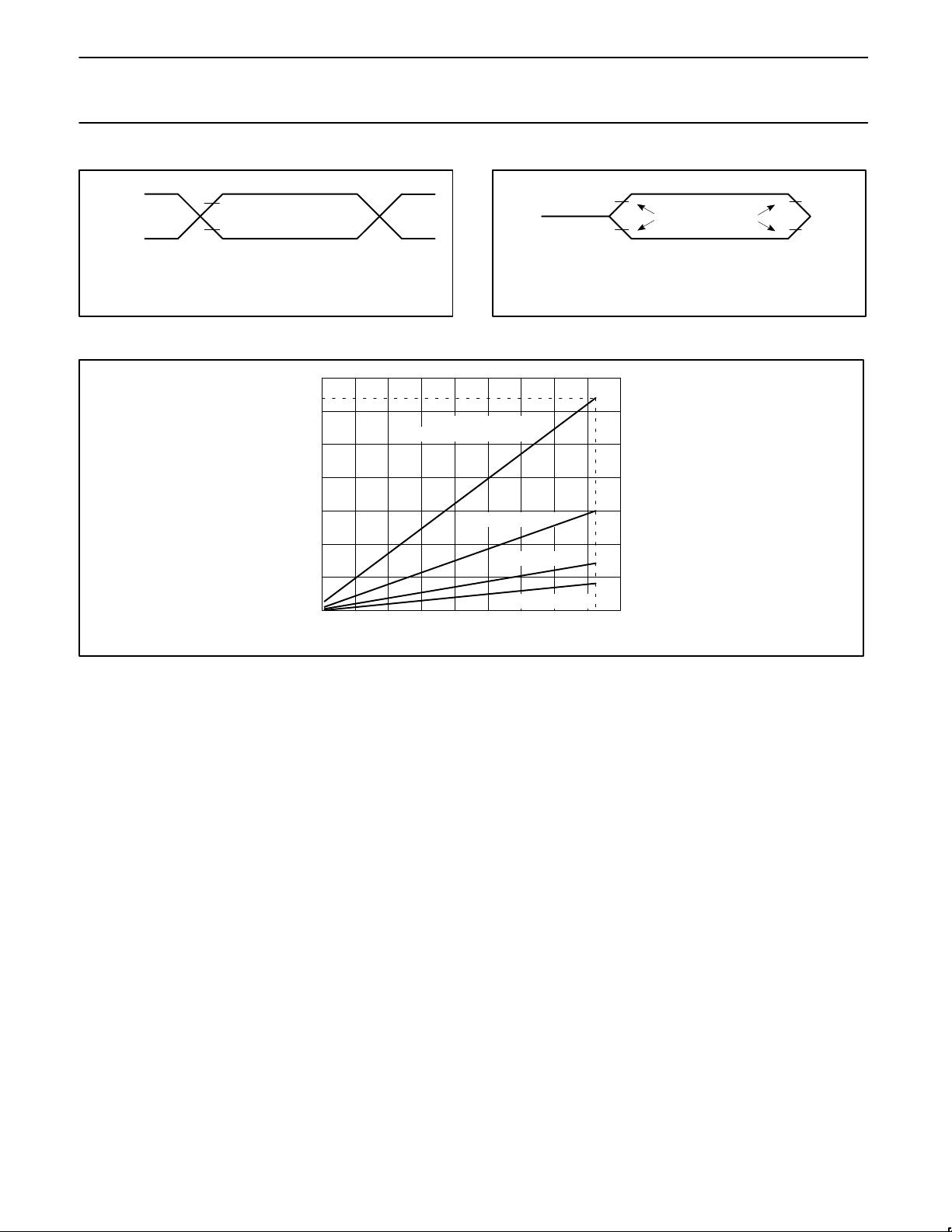
Philips Semiconductors Product specification
80C52/80C54/80C58CMOS single-chip 8-bit microcontrollers
VCC–0.5
0.45V
NOTE:
AC inputs during testing are driven at VCC –0.5 for a logic ‘1’ and 0.45V for a logic ‘0’.
Timing measurements are made at VIH min for a logic ‘1’ and VIL max for a logic ‘0’.
0.2V
0.2V
CC
CC
+0.9
–0.1
SU00717
Figure 18. AC Testing Input/Output
30
ICCMAX = 0.9 X FREQ. + 1.1
I
mA
25
20
CC
15
10
5
4MHz 8MHz 12MHz 16MHz
Figure 20. ICC vs. FREQ
Valid only within frequency specifications of the device under test
V
LOAD
NOTE:
For timing purposes, a port is no longer floating when a 100mV change from
load voltage occurs, and begins to float when a 100mV change from the loaded
level occurs. IOH/IOL ≥ ±20mA.
V
OH/VOL
MAX ACTIVE MODE
TYP ACTIVE MODE
MAX IDLE MODE
TYP IDLE MODE
20MHz3524MHz 28MHz 32MHz 36MHz
FREQ AT XTAL1
V
LOAD
V
LOAD
+0.1V
–0.1V
TIMING
REFERENCE
POINTS
Figure 19. Float Waveform
–0.1V
V
OH
V
+0.1V
OL
SU00718
SU00768
1996 Aug 16
24
Page 55
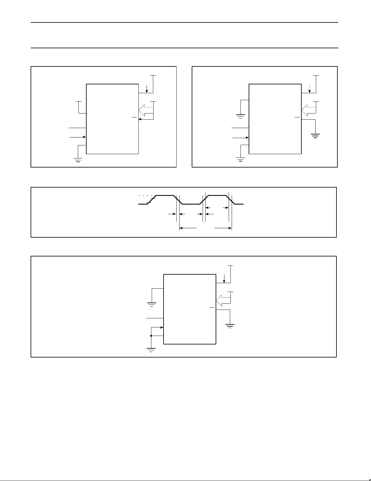
Philips Semiconductors Product specification
80C52/80C54/80C58CMOS single-chip 8-bit microcontrollers
V
CC
RST
(NC)
CLOCK SIGNAL
XTAL2
XTAL1
V
SS
Figure 21. ICC Test Condition, Active Mode
All other pins are disconnected
Figure 23. Clock Signal Waveform for ICC Tests in Active and Idle Modes
V
VCC–0.5
0.45V
P0
EA
V
CC
I
CC
CC
V
CC
SU00719
(NC)
CLOCK SIGNAL
RST
XTAL2
XTAL1
V
SS
V
EA
V
CC
I
CC
CC
V
CC
P0
SU00720
Figure 22. ICC Test Condition, Idle Mode
All other pins are disconnected
0.7V
CC
0.2VCC–0.1
t
CHCL
t
CLCH
= t
t
CLCX
CHCL
t
CLCL
= 5ns
t
CHCX
t
CLCH
SU00009
V
CC
I
CC
V
CC
V
CC
P0
(NC)
RST
XTAL2
XTAL1
V
SS
EA
Figure 24. ICC Test Condition, Power Down Mode
All other pins are disconnected. V
= 2V to 5.5V
CC
SU00016
1996 Aug 16
25
Page 56
Philips Semiconductors Product specification
80C52/80C54/80C58CMOS single-chip 8-bit microcontrollers
Security Bits
With none of the security bits programmed the code in the program
memory can be verified. If the encryption table is programmed, the
code will be encrypted when verified. When only security bit 1 (see
Table 8) is programmed, MOVC instructions executed from external
program memory are disabled from fetching code bytes from the
internal memory, EA
of the EPROM is disabled. When security bits 1 and 2 are
programmed, in addition to the above, verify mode is disabled.
Encryption Array
64 bytes of encryption array are initially unprogrammed (all 1s).
is latched on Reset and all further programming
Table 8. Program Security Bits
PROGRAM LOCK BITS
SB1 SB2 PROTECTION DESCRIPTION
1 U U No Program Security features enabled.
2 P U MOVC instructions executed from external program memory are disabled from fetching code bytes from
NOTES:
1. P – programmed. U – unprogrammed.
2. Any other combination of the security bits is not defined.
1, 2
(Code verify will still be encrypted by the Encryption Array if programmed.)
internal memory, EA
is sampled and latched on Reset, and further programming of the EPROM is disabled.
80C52 ROM CODE SUBMISSION
When submitting ROM code for the 80C52, the following must be specified:
1. 8k byte user ROM data
2. 64 byte ROM encryption key
3. ROM security bits.
ADDRESS
0000H to 1FFFH DATA 7:0 User ROM Data
2000H to 201FH KEY 7:0 ROM Encryption Key
2020H SEC 0 ROM Security Bit 1
2020H SEC 1 ROM Security Bit 2
CONTENT BIT(S) COMMENT
FFH = no encryption
0 = enable security
1 = disable security
0 = enable security
1 = disable security
Security Bit 1: When programmed, this bit has two effects on masked ROM parts:
1. External MOVC is disabled, and
2. EA
is latched on Reset.
Security Bit 2: When programmed, this bit inhibits Verify User ROM.
If the ROM Code file does not include the options, the following information must be included with the ROM code.
For each of the following, check the appropriate box, and send to Philips along with the code:
Security Bit #1:
Security Bit #2: Enabled Disabled
Encryption:
1996 Aug 16
Enabled Disabled
No Yes If Yes, must send key file.
26
Page 57
Philips Semiconductors Product specification
80C52/80C54/80C58CMOS single-chip 8-bit microcontrollers
80C54 ROM CODE SUBMISSION
When submitting ROM code for the 80C54, the following must be specified:
1. 16k byte user ROM data
2. 64 byte ROM encryption key
3. ROM security bits.
ADDRESS
0000H to 3FFFH DATA 7:0 User ROM Data
4000H to 401FH KEY 7:0 ROM Encryption Key
4020H SEC 0 ROM Security Bit 1
4020H SEC 1 ROM Security Bit 2
Security Bit 1: When programmed, this bit has two effects on masked ROM parts:
1. External MOVC is disabled, and
2. EA
is latched on Reset.
Security Bit 2: When programmed, this bit inhibits Verify User ROM.
If the ROM Code file does not include the options, the following information must be included with the ROM code.
For each of the following, check the appropriate box, and send to Philips along with the code:
Security Bit #1:
Security Bit #2: Enabled Disabled
Encryption:
Enabled Disabled
No Yes If Yes, must send key file.
CONTENT BIT(S) COMMENT
FFH = no encryption
0 = enable security
1 = disable security
0 = enable security
1 = disable security
1996 Aug 16
27
Page 58
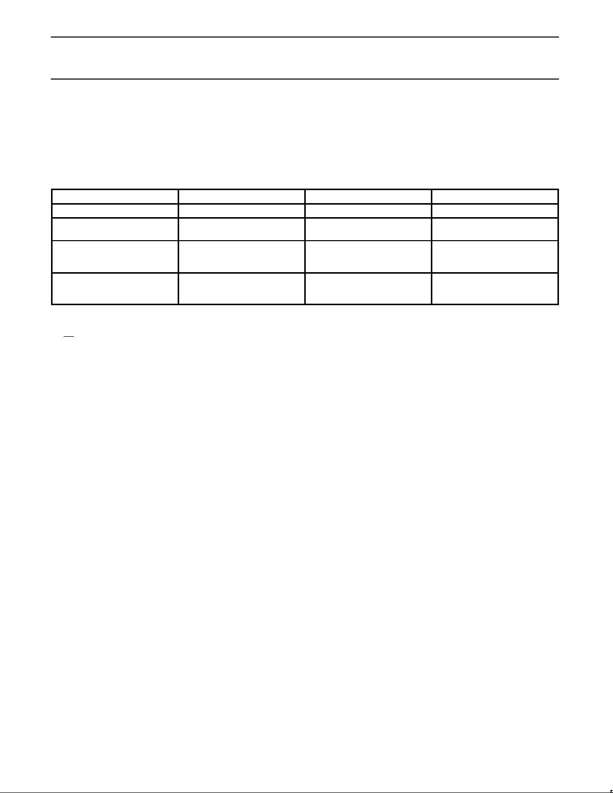
Philips Semiconductors Product specification
80C52/80C54/80C58CMOS single-chip 8-bit microcontrollers
80C58 ROM CODE SUBMISSION
When submitting ROM code for the 80C58, the following must be specified:
1. 32k byte user ROM data
2. 64 byte ROM encryption key
3. ROM security bits.
If submitting a file, the format is as follows:
ADDRESS CONTENT BIT(S) COMMENT
0000H to 7FFFH DATA 7:0 User ROM Data
8000H to 801FH KEY 7:0 ROM Encryption Key
8020H SEC 0 ROM Security Bit 1
8020H SEC 1 ROM Security Bit 2
FFH = no encryption
0 = enable security
1 = disable security
0 = enable security
1 = disable security
Security Bit 1: When programmed, this bit has two effects on masked ROM parts:
1. External MOVC is disabled, and
2. EA
is latched on Reset.
Security Bit 2: When programmed, this bit inhibits Verify User ROM.
If the ROM code file does not include the options, the following information must be included with the ROM code.
For each of the following check the appropriate box and send to Philips along with the code:
Security Bit #1:
Security Bit #2:
Encryption: No Yes If Yes, must send key file.
Enabled Disabled
Enabled Disabled
1996 Aug 16
28
Page 59
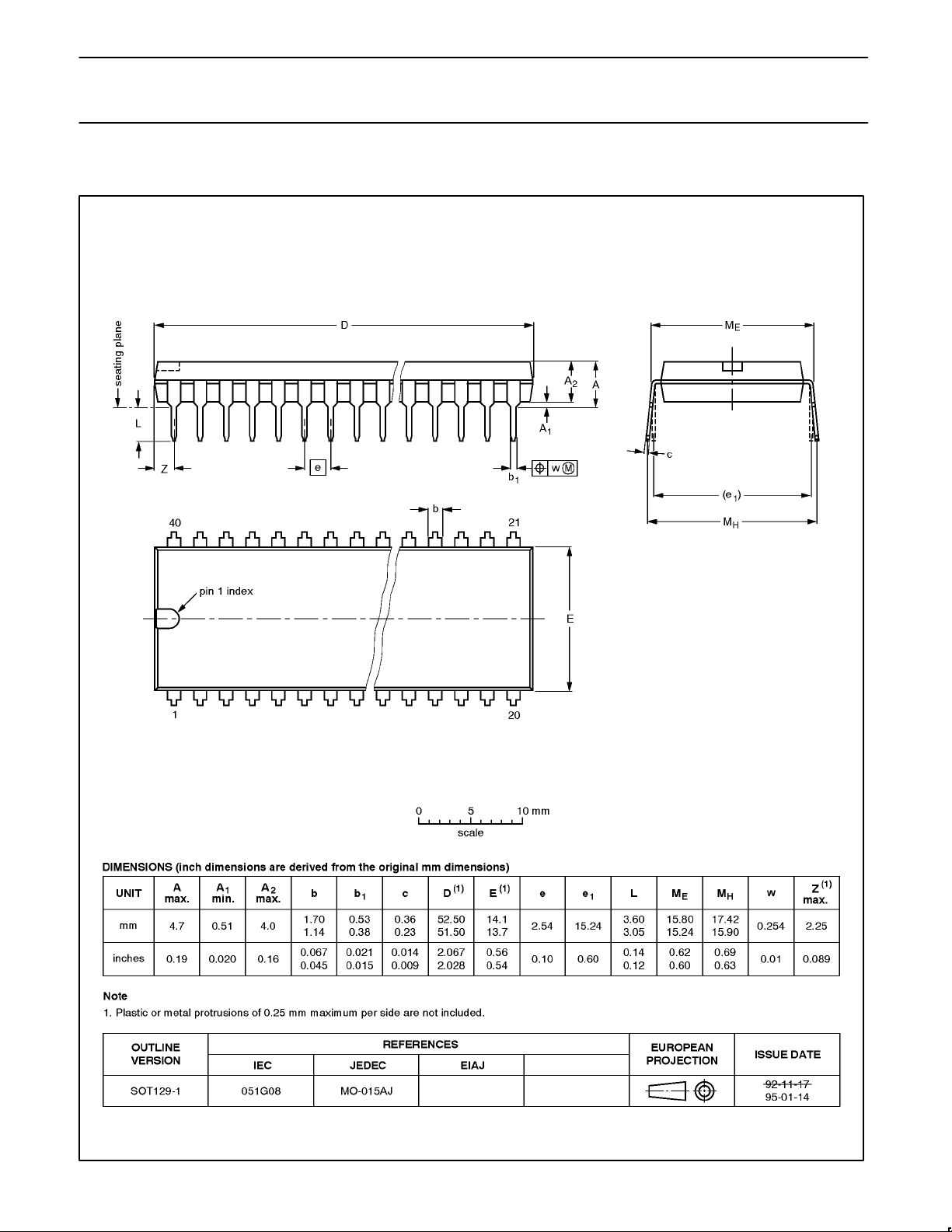
Philips Semiconductors Product specification
80C52/80C54/80C58CMOS single-chip 8-bit microcontrollers
DIP40: plastic dual in-line package; 40 leads (600 mil) SOT129-1
1996 Aug 16
29
Page 60
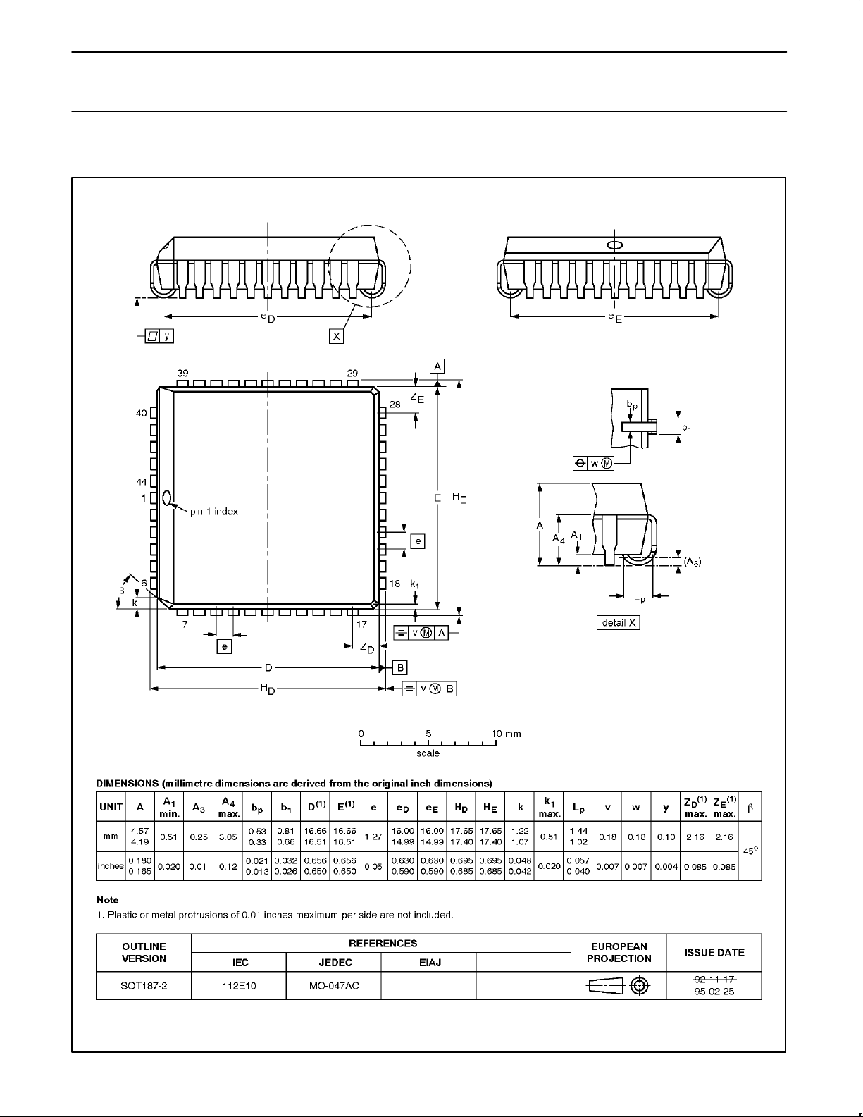
Philips Semiconductors Product specification
80C52/80C54/80C58CMOS single-chip 8-bit microcontrollers
PLCC44: plastic leaded chip carrier; 44 leads SOT187-2
1996 Aug 16
30
Page 61
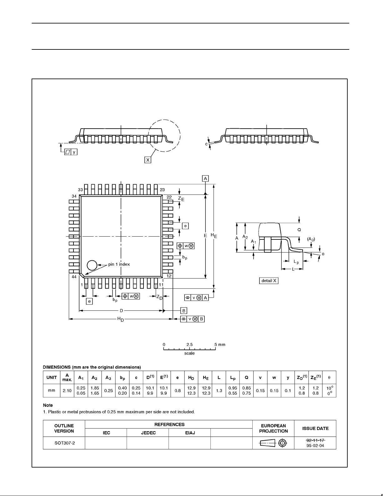
Philips Semiconductors Product specification
80C52/80C54/80C58CMOS single-chip 8-bit microcontrollers
QFP44: plastic quad flat package; 44 leads (lead length 1.3 mm); body 10 x 10 x 1.75 mm SOT307-2
1996 Aug 16
31
Page 62

Philips Semiconductors Product specification
80C52/80C54/80C58CMOS single-chip 8-bit microcontrollers
DEFINITIONS
Data Sheet Identification Product Status Definition
Objective Specification
Preliminary Specification
Product Specification
Formative or in Design
Preproduction Product
Full Production
Philips Semiconductors and Philips Electronics North America Corporation reserve the right to make changes, without notice, in the products,
including circuits, standard cells, and/or software, described or contained herein in order to improve design and/or performance. Philips
Semiconductors assumes no responsibility or liability for the use of any of these products, conveys no license or title under any patent, copyright,
or mask work right to these products, and makes no representations or warranties that these products are free from patent, copyright, or mask work
right infringement, unless otherwise specified. Applications that are described herein for any of these products are for illustrative purposes only.
Philips Semiconductors makes no representation or warranty that such applications will be suitable for the specified use without further testing or
modification.
LIFE SUPPORT APPLICATIONS
Philips Semiconductors and Philips Electronics North America Corporation Products are not designed for use in life support appliances, devices,
or systems where malfunction of a Philips Semiconductors and Philips Electronics North America Corporation Product can reasonably be expected
to result in a personal injury. Philips Semiconductors and Philips Electronics North America Corporation customers using or selling Philips
Semiconductors and Philips Electronics North America Corporation Products for use in such applications do so at their own risk and agree to fully
indemnify Philips Semiconductors and Philips Electronics North America Corporation for any damages resulting from such improper use or sale.
Philips Semiconductors
811 East Arques Avenue
P.O. Box 3409
Sunnyvale, California 94088–3409
Telephone 800-234-7381
This data sheet contains the design target or goal specifications for product development. Specifications
may change in any manner without notice.
This data sheet contains preliminary data, and supplementary data will be published at a later date. Philips
Semiconductors reserves the right to make changes at any time without notice in order to improve design
and supply the best possible product.
This data sheet contains Final Specifications. Philips Semiconductors reserves the right to make changes
at any time without notice, in order to improve design and supply the best possible product.
Philips Semiconductors and Philips Electronics North America Corporation
register eligible circuits under the Semiconductor Chip Protection Act.
Copyright Philips Electronics North America Corporation 1996
All rights reserved. Printed in U.S.A.
 Loading...