

Page 1
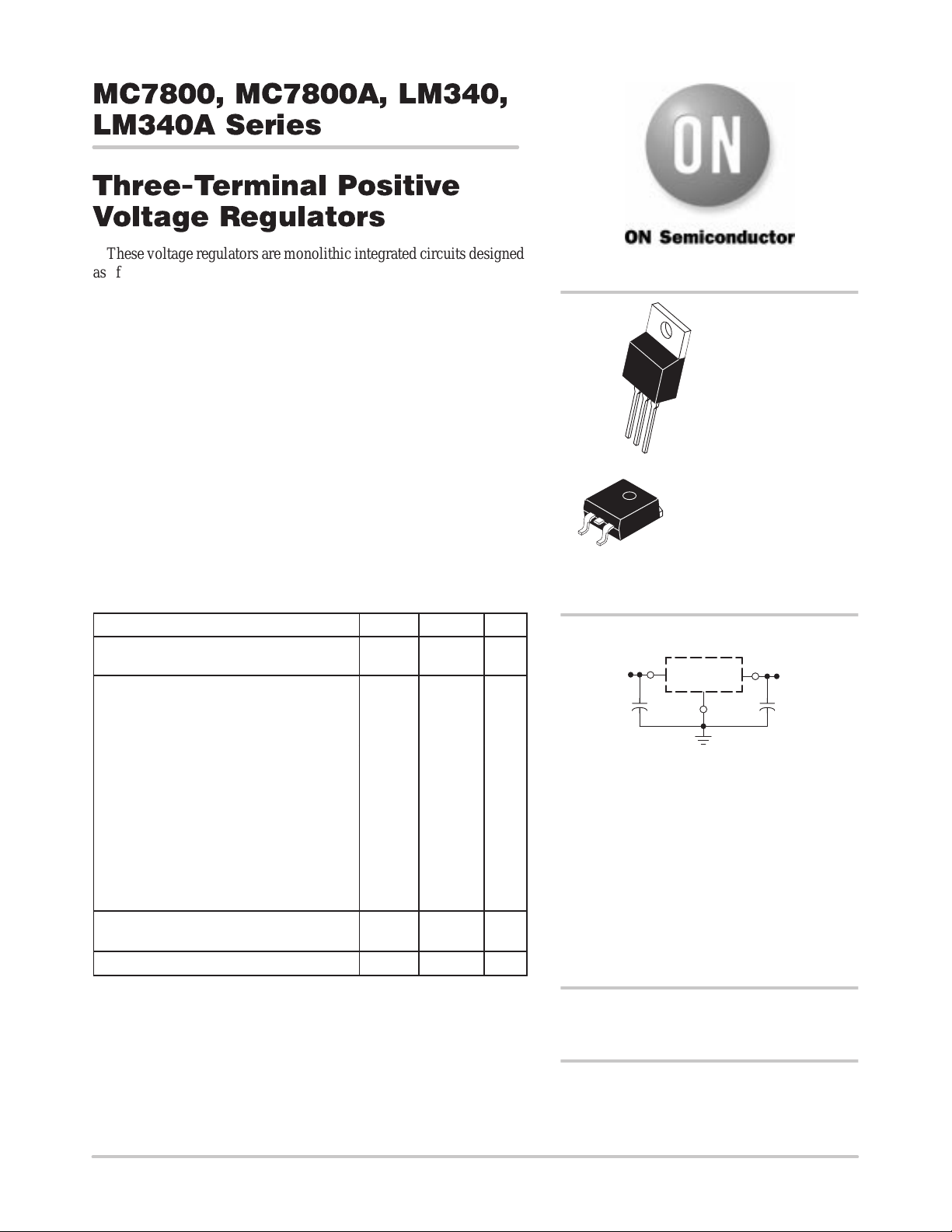
MC7800, MC7800A, LM340,
LM340A Series
Three-Terminal Positive
V oltage Regulators
These voltage regulators are monolithic integrated circuits designed
as fixed–voltage regulators for a wide variety of applications
including local, on–card regulation. These regulators employ internal
current limiting, thermal shutdown, and safe–area compensation. With
adequate heatsinking they can deliver output currents in excess of
1.0 A. Although designed primarily as a fixed voltage regulator, these
devices can be used with external components to obtain adjustable
voltages and currents.
• Output Current in Excess of 1.0 A
• No External Components Required
• Internal Thermal Overload Protection
• Internal Short Circuit Current Limiting
• Output T ransistor Safe–Area Compensation
• Output Voltage Offered in 2% and 4% Tolerance
• Available in Surface Mount D
Packages
MAXIMUM RATINGS (T
Input Voltage (5.0 – 18 V) V
Input Voltage (24 V) 40
Power Dissipation
Case 221A
TA = 25°C P
Thermal Resistance, Junction–to–Ambient R
Thermal Resistance, Junction–to–Case R
Case 936 (D2PAK)
TA = 25°C P
Thermal Resistance, Junction–to–Ambient R
Thermal Resistance, Junction–to–Case R
Storage Junction Temperature Range T
Operating Junction Temperature T
NOTE: ESD data available upon request.
A
Rating
2
PAK and Standard 3–Lead Transistor
= 25°C, unless otherwise noted.)
Symbol Value Unit
I
Internally
D
θJA
θJC
Internally
D
θJA
θJA
stg
J
35 Vdc
Limited
65 °C/W
5.0 °C/W
Limited
See
Figure
13
5.0 °C/W
–65 to
+150
+150 °C
W
W
°C/W
°C
http://onsemi.com
TO–220
T SUFFIX
CASE 221A
Heatsink surface
1
2
3
2
1
3
Heatsink surface (shown as terminal 4 in
case outline drawing) is connected to Pin 2.
connected to Pin 2.
D2PAK
D2T SUFFIX
CASE 936
Pin 1. Input
2. Ground
3. Output
STANDARD APPLICATION
Input
Cin*
0.33 µF
A common ground is required between the
input and the output voltages. The input voltage
must remain typically 2.0 V above the output
voltage even during the low point on the input
ripple voltage.
XX,
These two digits of the type number
indicate nominal voltage.
Cin is required if regulator is located an
*
appreciable distance from power supply
filter.
CO is not needed for stability; however,
**
it does improve transient response. Values
of less than 0.1 µF could cause instability.
MC78XX
Output
CO**
ORDERING INFORMATION
See detailed ordering and shipping information in the package
dimensions section on page 16 of this data sheet.
Semiconductor Components Industries, LLC, 2000
April, 2000 – Rev. 6
DEVICE MARKING INFORMATION
See general marking information in the device marking
section on page 18 of this data sheet.
1 Publication Order Number:
MC7800/D
Page 2
R18
100 k
D1
Zener
Q7
QNPN
R17
9.0 k
R1
10.66 k
R2
1.56 k
Q8
QNPN
MC7800, MC7800A, LM340, LM340A Series
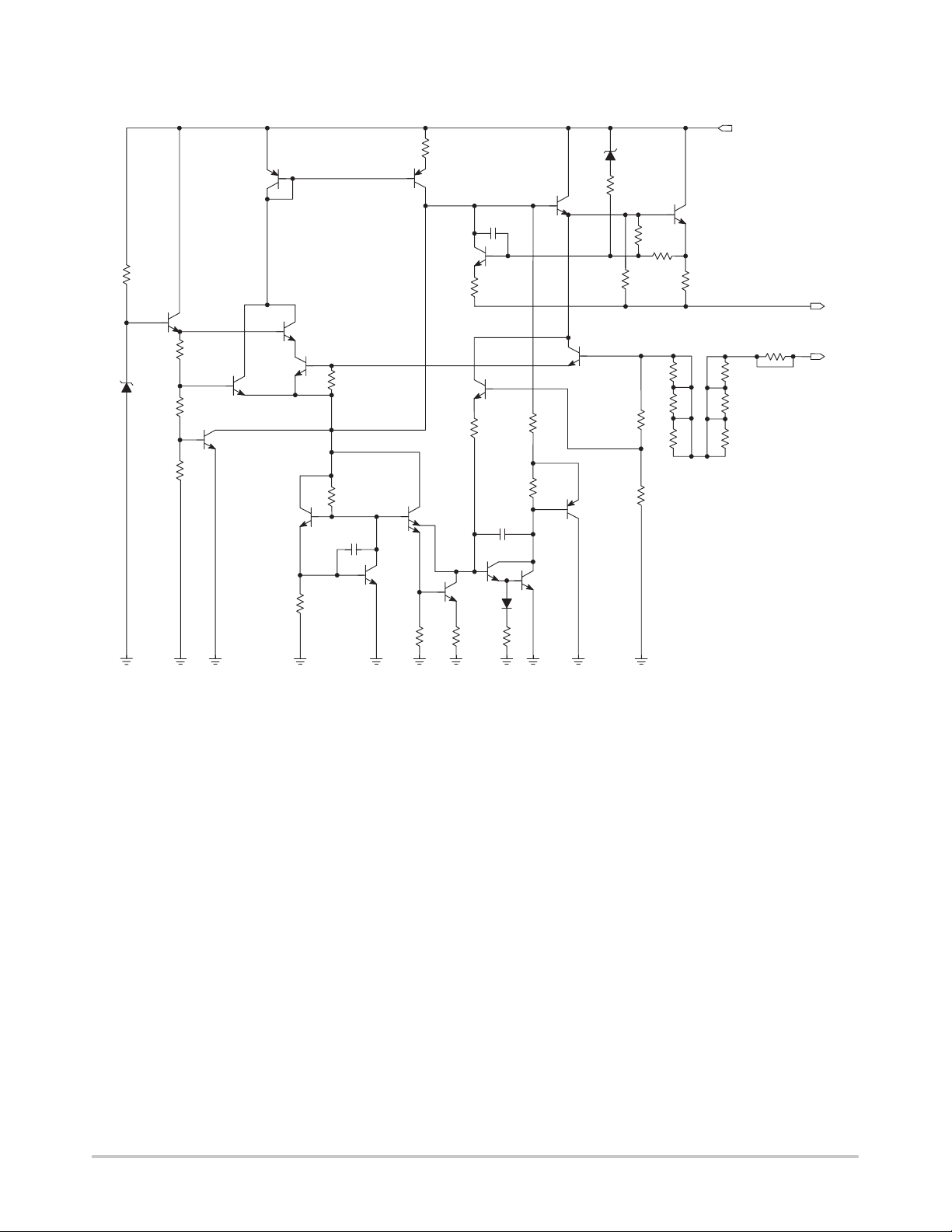
Representative Schematic Diagram
LAT
Q17
Q6
QNPN
QNPN 2
QNPN
Q9
Q14
Q5
QNPN 2
R6
1.0 k
MC7800
R11
15 k
R5
4.5 k
C2
3.0 P
Q13
QNPN
QNPN 6
R24
50
LAT 3 A
Q18
QNPN
QNPN
Q1
R7
14 kR31.8 k
Q10
Q15
Q2
QNPN 4
C3
R22
100
R20
17500
N+
Q4
QNPN
Q16
Diode
1.0 P
C1
30 P
R8
5.0 k
QNPN
R16
600
R9
3.0 k
Q3
QNPN
Q12
Q19
QNPN
R21
600
3340–(3316ACT)
SUB
Q11 2
D2
Zener
R19
27.5 k
R10
R14
1.0 k
3.0 k
6.0 k
3.0 k
R13
11660
R12
R25
R26
R15
680
Q20
QNPN
R23
0.2
V
R29
9.0 k
R28
9.0 k
R27
9.0 k
in
V
out
5.01
R30
18 k
Sense
This device contains 22 active transistors.
http://onsemi.com
2
Page 3
MC7800, MC7800A, LM340, LM340A Series
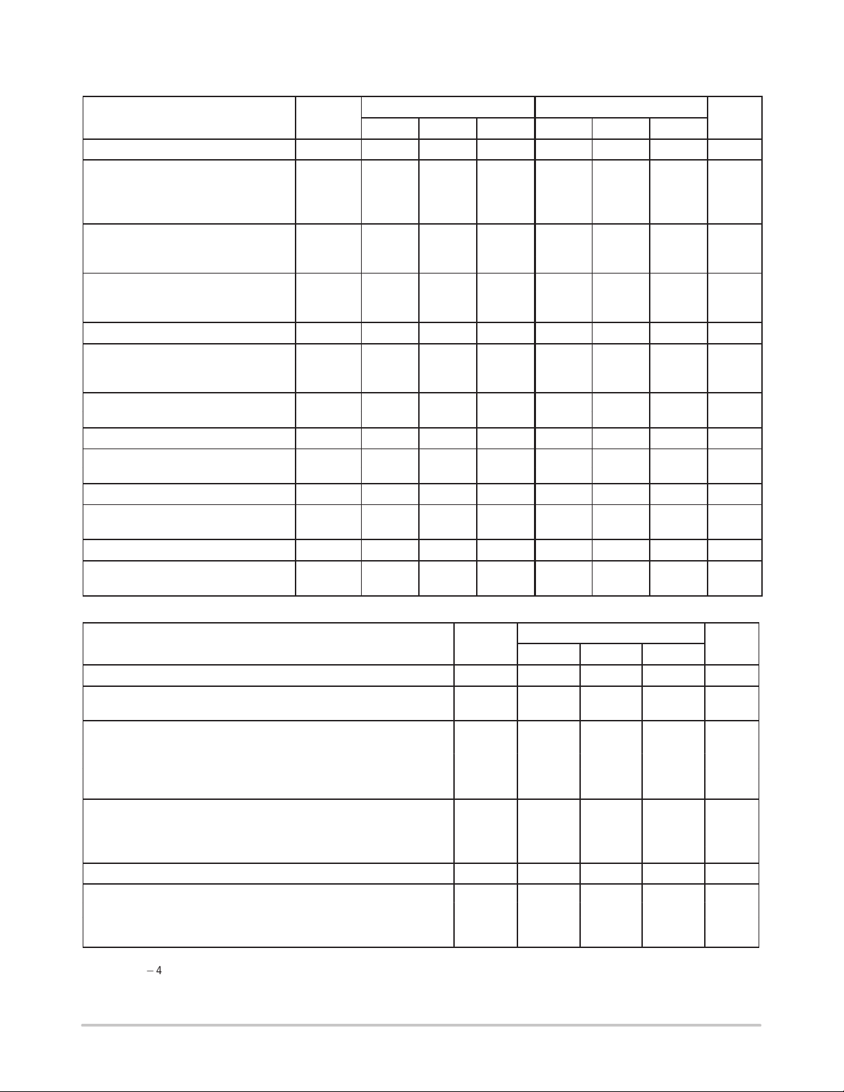
ELECTRICAL CHARACTERISTICS (V
Characteristic Symbol Min Typ Max Min Typ Max Unit
Output Voltage (TJ = 25°C) V
Output Voltage (5.0 mA ≤ IO ≤ 1.0 A, P
≤ 15 W)
7.0 Vdc ≤ Vin ≤ 20 Vdc – – – 4.75 5.0 5.25
8.0 Vdc ≤ Vin ≤ 20 Vdc 4.75 5.0 5.25 – – –
Line Regulation (Note 2.) Reg
7.5 Vdc ≤ Vin ≤ 20 Vdc, 1.0 A – 5.0 100 – 0.5 20
8.0 Vdc ≤ Vin ≤ 12 Vdc – 1.3 50 – 0.8 10
Load Regulation (Note 2.) Reg
5.0 mA ≤ IO ≤ 1.0 A – 1.3 100 – 1.3 25
5.0 mA ≤ IO ≤ 1.5 A (TA = 25°C) – 0.15 50 – 1.3 25
Quiescent Current I
Quiescent Current Change ∆I
7.0 Vdc ≤ Vin ≤ 25 Vdc – – – – 0.3 1.0
5.0 mA ≤ IO ≤ 1.0 A (TA = 25°C) – – 0.5 – 0.08 0.8
Ripple Rejection RR – 68 – 62 83 – dB
8.0 Vdc ≤ Vin ≤ 18 Vdc, f = 120 Hz
Dropout Voltage (IO = 1.0 A, TJ = 25°C) VI – V
Output Noise Voltage (TA = 25°C) V
10 Hz ≤ f ≤ 100 kHz
Output Resistance f = 1.0 kHz r
Short Circuit Current Limit (TA = 25°C) I
Vin = 35 Vdc
Peak Output Current (TJ = 25°C) I
Average Temperature Coefficient of
Output Voltage
= 10 V, IO = 500 mA, TJ = T
in
O
V
D
SC
max
TCV
O
line
load
B
B
O
n
O
O
to T
low
MC7805B MC7805C/LM340T–5
4.8 5.0 5.2 4.8 5.0 5.2 Vdc
– 3.2 8.0 – 3.2 6.5 mA
– 2.0 – – 2.0 – Vdc
– 10 – – 10 – µV/V
– 0.9 – – 0.9 – mΩ
– 0.2 – – 0.6 – A
– 2.2 – – 2.2 – A
– –0.3 – – –0.3 – mV/°C
[Note 1.], unless otherwise noted.)
high
Vdc
mV
mV
mA
O
ELECTRICAL CHARACTERISTICS (V
Characteristic Symbol Min Typ Max Unit
Output Voltage (TJ = 25°C) V
Output Voltage (5.0 mA ≤ IO ≤ 1.0 A, PD ≤ 15 W) V
7.5 Vdc ≤ Vin ≤ 20 Vdc
Line Regulation (Note 2.) Reg
7.5 Vdc ≤ Vin ≤ 25 Vdc, IO = 500 mA – 0.5 10
8.0 Vdc ≤ Vin ≤ 12 Vdc, IO = 1.0 A – 0.8 12
8.0 Vdc ≤ Vin ≤ 12 Vdc, IO = 1.0 A, TJ = 25°C – 1.3 4.0
7.3 Vdc ≤ Vin ≤ 20 Vdc, IO = 1.0 A, TJ = 25°C – 4.5 10
Load Regulation (Note 2.) Reg
5.0 mA ≤ IO ≤ 1.5 A, TJ = 25°C – 1.3 25
5.0 mA ≤ IO ≤ 1.0 A – 0.8 25
250 mA ≤ IO ≤ 750 mA – 0.53 15
Quiescent Current I
Quiescent Current Change ∆I
8.0 Vdc ≤ Vin ≤ 25 Vdc, IO = 500 mA – 0.3 0.8
7.5 Vdc ≤ Vin ≤ 20 Vdc, TJ = 25°C – – 0.8
5.0 mA ≤ IO ≤ 1.0 A – 0.08 0.5
1. T
2. Load and line regulation are specified at constant junction temperature. Changes in VO due to heating effects must be taken into account
=0°C for MC78XXAC, C, LM340AT–XX, LM340T–XX T
low
=*40°C for MC78XXB
separately . Pulse testing with low duty cycle is used.
= 10 V, IO = 1.0 A, TJ = T
in
low
high
to T
[Note 1.], unless otherwise noted.)
high
MC7805AC/LM340AT–5
O
O
line
load
B
B
= +125°C for MC78XXAC, C, LM340AT–XX, LM340T–XX
4.9 5.0 5.1 Vdc
4.8 5.0 5.2 Vdc
– 3.2 6.0 mA
mV
mV
mA
http://onsemi.com
3
Page 4
MC7800, MC7800A, LM340, LM340A Series
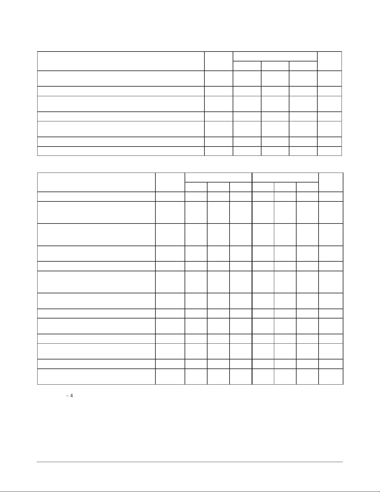
ELECTRICAL CHARACTERISTICS (continued) (V
otherwise noted.)
Characteristic Symbol Min Typ Max Unit
Ripple Rejection RR 68 83 – dB
8.0 Vdc ≤ Vin ≤ 18 Vdc, f = 120 Hz, IO = 500 mA
Dropout Voltage (IO = 1.0 A, TJ = 25°C) VI – V
Output Noise Voltage (TA = 25°C) V
10 Hz ≤ f ≤ 100 kHz
Output Resistance (f = 1.0 kHz) r
Short Circuit Current Limit (TA = 25°C) I
Vin = 35 Vdc
Peak Output Current (TJ = 25°C) I
Average Temperature Coefficient of Output Voltage TCV
ELECTRICAL CHARACTERISTICS (V
Characteristic Symbol Min Typ Max Min Typ Max Unit
Output Voltage (TJ = 25°C) V
Output Voltage (5.0 mA ≤ IO ≤ 1.0 A, PD ≤ 15 W) V
8.0 Vdc ≤ Vin ≤ 21 Vdc – – – 5.7 6.0 6.3
9.0 Vdc ≤ Vin ≤ 21 Vdc 5.7 6.0 6.3 – – –
Line Regulation, TJ = 25°C (Note 2.) Reg
8.0 Vdc ≤ Vin ≤ 25 Vdc – 5.5 120 – 0.5 24
9.0 Vdc ≤ Vin ≤ 13 Vdc – 1.4 60 – 0.8 12
Load Regulation, TJ = 25°C (Note 2.) Reg
5.0 mA ≤ IO ≤ 1.5 A
Quiescent Current (TJ = 25°C) I
Quiescent Current Change ∆I
8.0 Vdc ≤ Vin ≤ 25 Vdc – – – – 0.3 1.3
5.0 mA ≤ IO ≤ 1.0 A – – 0.5 – 0.08 0.5
Ripple Rejection RR – 65 – 58 65 – dB
9.0 Vdc ≤ Vin ≤ 19 Vdc, f = 120 Hz
Dropout Voltage (IO = 1.0 A, TJ = 25°C) VI – V
Output Noise Voltage (TA = 25°C) V
10 Hz ≤ f ≤ 100 kHz
Output Resistance f = 1.0 kHz r
Short Circuit Current Limit (TA = 25°C) I
Vin = 35 Vdc
Peak Output Current (TJ = 25°C) I
Average Temperature Coefficient of Output
Voltage
1. T
2. Load and line regulation are specified at constant junction temperature. Changes in VO due to heating effects must be taken into account
=0°C for MC78XXAC, C, LM340AT–XX, LM340T–XX T
low
=*40°C for MC78XXB
separately . Pulse testing with low duty cycle is used.
= 11 V, IO = 500 mA, TJ = T
in
= 10 V, IO = 1.0 A, TJ = T
in
low
O
O
line
load
B
B
n
O
SC
max
TCV
5.75 6.0 6.25 5.75 6.0 6.25 Vdc
– 1.3 120 – 1.3 30 mV
– 3.3 8.0 – 3.3 8.0 mA
O
O
– 2.0 – – 2.0 – Vdc
– 10 – – 10 – µV/V
– 0.9 – – 0.9 – mΩ
– 0.2 – – 0.2 – A
– 2.2 – – 2.2 – A
– –0.3 – – –0.3 – mV/°C
high
to T
low
O
n
O
SC
max
O
to T
MC7806B MC7806C
= +125°C for MC78XXAC, C, LM340AT–XX, LM340T–XX
[Note 1.], unless otherwise noted.)
high
[Note 1.], unless
high
MC7805AC/LM340A T–5
– 2.0 – Vdc
– 10 – µV/V
– 0.9 – mΩ
– 0.2 – A
– 2.2 – A
– –0.3 – mV/°C
Vdc
mV
mA
O
O
http://onsemi.com
4
Page 5
MC7800, MC7800A, LM340, LM340A Series
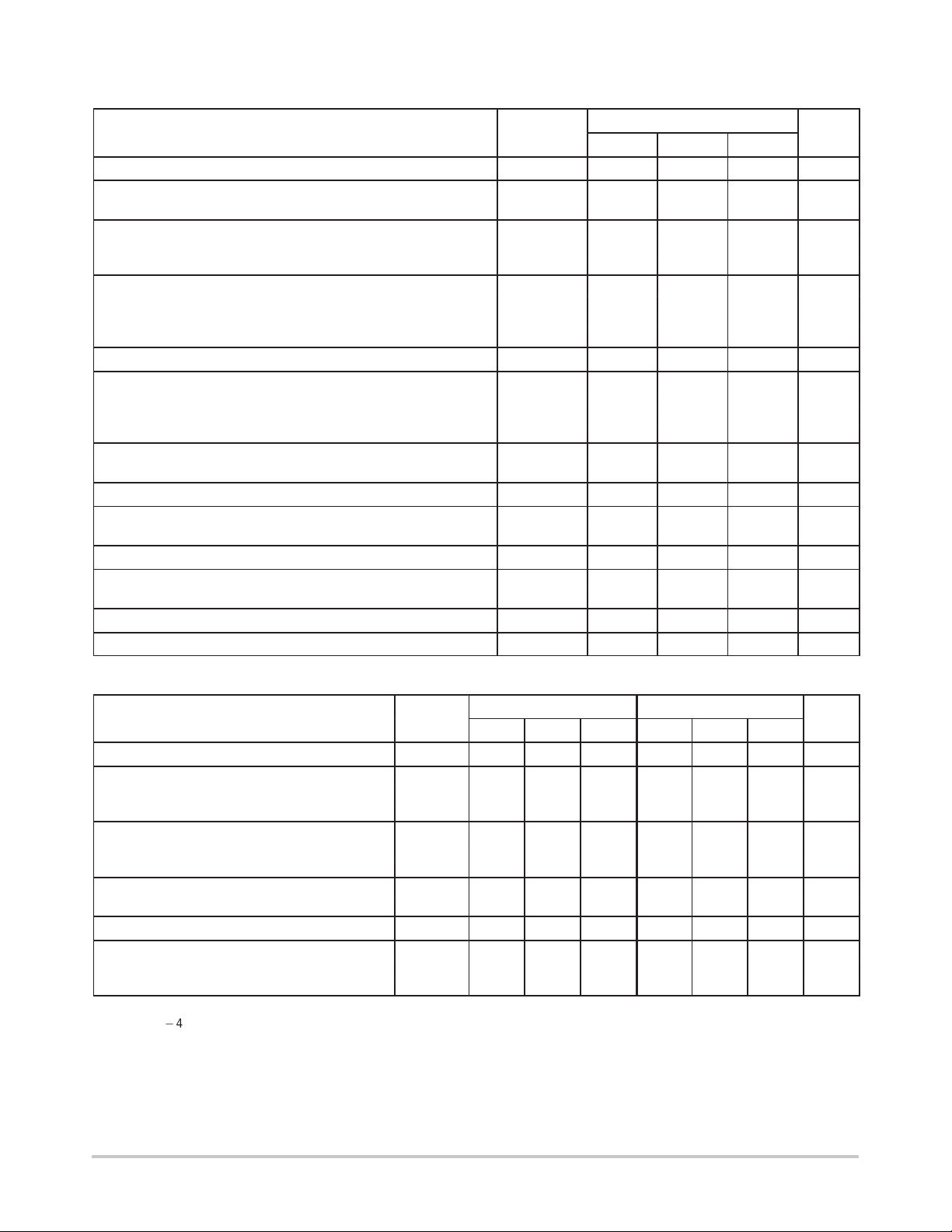
ELECTRICAL CHARACTERISTICS (V
Characteristic Symbol Min Typ Max Unit
Output Voltage (TJ = 25°C) V
Output Voltage (5.0 mA ≤ IO ≤ 1.0 A, PD ≤ 15 W) V
8.6 Vdc ≤ Vin ≤ 21 Vdc
Line Regulation (Note 2.) Reg
8.6 Vdc ≤ Vin ≤ 25 Vdc, IO = 500 mA – 5.0 12
9.0 Vdc ≤ Vin ≤ 13 Vdc, IO = 1.0 A – 1.4 15
Load Regulation (Note 2.) Reg
5.0 mA ≤ IO ≤ 1.5 A, TJ = 25°C – 1.3 25
5.0 mA ≤ IO ≤ 1.0 A – 0.9 25
250 mA ≤ IO ≤ 750 mA – 0.2 15
Quiescent Current I
Quiescent Current Change ∆I
9.0 Vdc ≤ Vin ≤ 25 Vdc, IO = 500 mA – – 0.8
9.0 Vdc ≤ Vin ≤ 21 Vdc, IO = 1.0 A, TJ = 25°C – – 0.8
5.0 mA ≤ IO ≤ 1.0 A – – 0.5
Ripple Rejection RR 58 65 – dB
9.0 Vdc ≤ Vin ≤ 19 Vdc, f = 120 Hz, IO = 500 mA
Dropout Voltage (IO = 1.0 A, TJ = 25°C) VI – V
Output Noise Voltage (TA = 25°C) V
10 Hz ≤ f ≤ 100 kHz
Output Resistance (f = 1.0 kHz) r
Short Circuit Current Limit (TA = 25°C) I
Vin = 35 Vdc
Peak Output Current (TJ = 25°C) I
Average Temperature Coefficient of Output Voltage TCV
= 11 V, IO = 1.0 A, TJ = T
in
low
to T
[Note 1.], unless otherwise noted.)
high
MC7806AC
O
O
line
load
B
B
O
n
O
SC
max
O
5.88 6.0 6.12 Vdc
5.76 6.0 6.24 Vdc
– 3.3 6.0 mA
– 2.0 – Vdc
– 10 – µV/V
– 0.9 – mΩ
– 0.2 – A
– 2.2 – A
– –0.3 – mV/°C
mV
mV
mA
O
ELECTRICAL CHARACTERISTICS (V
Characteristic Symbol Min Typ Max Min Typ Max Unit
Output Voltage (TJ = 25°C) V
Output Voltage (5.0 mA ≤ IO ≤ 1.0 A, PD ≤ 15 W) V
10.5 Vdc ≤ Vin ≤ 23 Vdc – – – 7.6 8.0 8.4
11.5 Vdc ≤ Vin ≤ 23 Vdc 7.6 8.0 8.4 – – –
Line Regulation, TJ = 25°C, (Note 2.) Reg
10.5 Vdc ≤ Vin ≤ 25 Vdc – 6.0 160 – 6.0 32
11 Vdc ≤ Vin ≤ 17 Vdc – 1.7 80 – 1.7 16
Load Regulation, TJ = 25°C (Note 2.) Reg
5.0 mA ≤ IO ≤ 1.5 A
Quiescent Current I
Quiescent Current Change ∆I
10.5 Vdc ≤ Vin ≤ 25 Vdc – – – – – 1.0
5.0 mA ≤ IO ≤ 1.0 A – – 0.5 – – 0.5
1. T
2. Load and line regulation are specified at constant junction temperature. Changes in VO due to heating effects must be taken into account
=0°C for MC78XXAC, C, LM340AT–XX, LM340T–XX T
low
=*40°C for MC78XXB
separately . Pulse testing with low duty cycle is used.
= 14 V, IO = 500 mA, TJ = T
in
O
O
line
load
B
B
to T
low
MC7808B MC7808C
7.7 8.0 8.3 7.7 8.0 8.3 Vdc
– 1.4 160 – 1.4 35 mV
– 3.3 8.0 – 3.3 8.0 mA
= +125°C for MC78XXAC, C, LM340AT–XX, LM340T–XX
high
[Note 1.], unless otherwise noted.)
high
Vdc
mV
mA
http://onsemi.com
5
Page 6
MC7800, MC7800A, LM340, LM340A Series
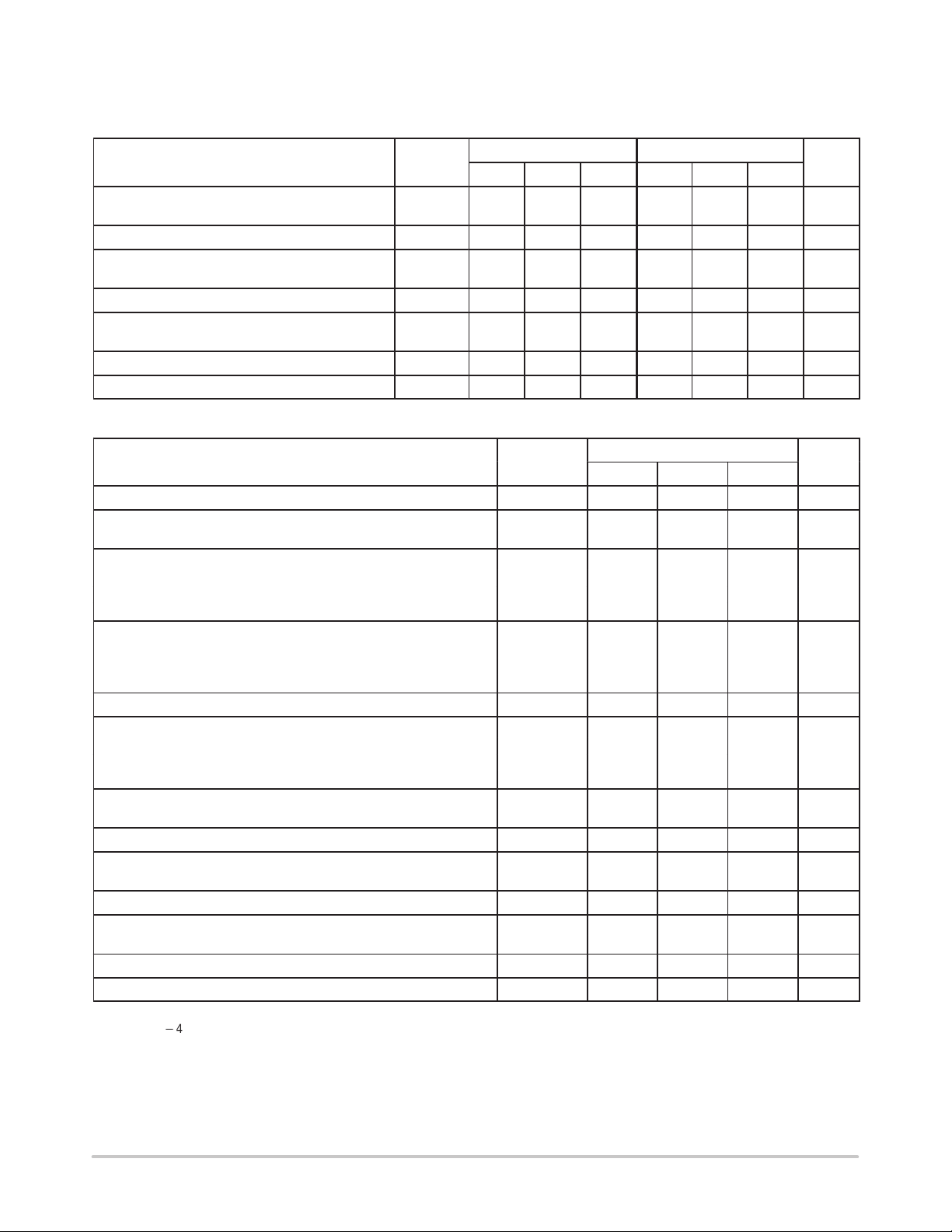
ELECTRICAL CHARACTERISTICS (continued) (V
otherwise noted.)
Characteristic Symbol Min Typ Max Min Typ Max Unit
Ripple Rejection RR – 62 – 56 62 – dB
11.5 Vdc ≤ Vin ≤ 18 Vdc, f = 120 Hz
Dropout Voltage (IO = 1.0 A, TJ = 25°C) VI – V
Output Noise Voltage (TA = 25°C) V
10 Hz ≤ f ≤ 100 kHz
Output Resistance f = 1.0 kHz r
Short Circuit Current Limit (TA = 25°C) I
Vin = 35 Vdc
Peak Output Current (TJ = 25°C) I
Average Temperature Coefficient of Output Voltage TCV
ELECTRICAL CHARACTERISTICS (V
Characteristic Symbol Min Typ Max Unit
Output Voltage (TJ = 25°C) V
Output Voltage (5.0 mA ≤ IO ≤ 1.0 A, PD ≤ 15 W) V
10.6 Vdc ≤ Vin ≤ 23 Vdc
Line Regulation (Note 2.) Reg
10.6 Vdc ≤ Vin ≤ 25 Vdc, IO = 500 mA – 6.0 15
11 Vdc ≤ Vin ≤ 17 Vdc, IO = 1.0 A – 1.7 18
10.4 Vdc ≤ Vin ≤ 23 Vdc, TJ = 25°C – 5.0 15
Load Regulation (Note 2.) Reg
5.0 mA ≤ IO ≤ 1.5 A, TJ = 25°C – 1.4 25
5.0 mA ≤ IO ≤ 1.0 A – 1.0 25
250 mA ≤ IO ≤ 750 mA – 0.22 15
Quiescent Current I
Quiescent Current Change ∆I
11 Vdc ≤ Vin ≤ 25 Vdc, IO = 500 mA – – 0.8
10.6 Vdc ≤ Vin ≤ 23 Vdc, IO = 1.0 A, TJ = 25°C – – 0.8
5.0 mA ≤ IO ≤ 1.0 A – – 0.5
Ripple Rejection RR 56 62 – dB
11.5 Vdc ≤ Vin ≤ 21.5 Vdc , f = 120 Hz, IO = 500 mA
Dropout Voltage (IO = 1.0 A, TJ = 25°C) VI – V
Output Noise Voltage (TA = 25°C) V
10 Hz ≤ f ≤ 100 kHz
Output Resistance f = 1.0 kHz r
Short Circuit Current Limit (TA = 25°C) I
Vin = 35 Vdc
Peak Output Current (TJ = 25°C) I
Average Temperature Coefficient of Output Voltage TCV
1. T
2. Load and line regulation are specified at constant junction temperature. Changes in VO due to heating effects must be taken into account
=0°C for MC78XXAC, C, LM340AT–XX, LM340T–XX T
low
=*40°C for MC78XXB
separately . Pulse testing with low duty cycle is used.
= 14 V, IO = 1.0 A, TJ = T
in
= 14 V, IO = 500 mA, TJ = T
in
MC7808B MC7808C
O
n
O
SC
max
O
– 2.0 – – 2.0 – Vdc
– 10 – – 10 – µV/V
– 0.9 – – 0.9 – mΩ
– 0.2 – – 0.2 – A
– 2.2 – – 2.2 – A
– –0.4 – – –0.4 – mV/°C
to T
low
high
O
O
line
load
B
B
n
O
SC
max
O
= +125°C for MC78XXAC, C, LM340AT–XX, LM340T–XX
high
to T
low
[Note 1.], unless otherwise noted.)
7.84 8.0 8.16 Vdc
O
[Note 1.], unless
high
MC7808AC
7.7 8.0 8.3 Vdc
– 3.3 6.0 mA
– 2.0 – Vdc
– 10 – µV/V
– 0.9 – mΩ
– 0.2 – A
– 2.2 – A
– –0.4 – mV/°C
O
mV
mV
mA
O
http://onsemi.com
6
Page 7
MC7800, MC7800A, LM340, LM340A Series
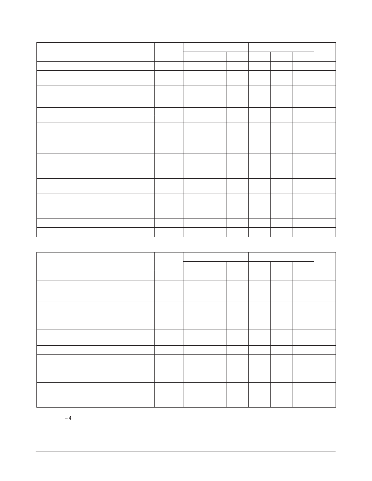
ELECTRICAL CHARACTERISTICS (V
Characteristic Symbol Min Typ Max Min Typ Max Unit
Output Voltage (TJ = 25°C) V
Output Voltage (5.0 mA ≤ IO ≤ 1.0 A, PD ≤ 15 W) V
11.5 Vdc ≤ Vin ≤ 24 Vdc 8.55 9.0 9.45 8.55 9.0 9.45
Line Regulation, TJ = 25°C (Note 2.) Reg
11 Vdc ≤ Vin ≤ 26 Vdc – 6.2 32 – 6.2 32
11.5 Vdc ≤ Vin ≤ 17 Vdc – 1.8 16 – 1.8 16
Load Regulation, TJ = 25°C (Note 2.) Reg
5.0 mA ≤ IO ≤ 1.5 A
Quiescent Current I
Quiescent Current Change ∆I
11.5 Vdc ≤ Vin ≤ 26 Vdc – – 1.0 – – 1.0
5.0 mA ≤ IO ≤ 1.0 A – – 0.5 – – 0.5
Ripple Rejection RR 56 61 – 56 61 – dB
11.5 Vdc ≤ Vin ≤ 21.5 Vdc, f = 120 Hz
Dropout Voltage (IO = 1.0 A, TJ = 25°C) VI – V
Output Noise Voltage (TA = 25°C) V
10 Hz ≤ f ≤ 100 kHz
Output Resistance f = 1.0 kHz r
Short Circuit Current Limit (TA = 25°C) I
Vin = 35 Vdc
Peak Output Current (TJ = 25°C) I
Average Temperature Coefficient of Output Voltage TCV
= 15 V, IO = 500 mA, TJ = T
in
O
O
line
load
B
B
O
n
O
SC
max
O
to T
low
MC7809BT MC7809CT
8.65 9.0 9.35 8.65 9.0 9.35 Vdc
– 1.5 35 – 1.5 35 mV
– 3.4 8.0 – 3.4 8.0 mA
– 2.0 – – 2.0 – Vdc
– 10 – – 10 – µV/V
– 1.0 – – 1.0 – mΩ
– 0.2 – – 0.2 – A
– 2.2 – – 2.2 – A
– –0.5 – – –0.5 – mV/°C
[Note 1.], unless otherwise noted.)
high
Vdc
mV
mA
O
ELECTRICAL CHARACTERISTICS (V
Characteristic Symbol Min Typ Max Min Typ Max Unit
Output Voltage (TJ = 25°C) V
Output Voltage (5.0 mA ≤ IO ≤ 1.0 A, PD ≤ 15 W) V
14.5 Vdc ≤ Vin ≤ 27 Vdc – – – 11.4 12 12.6
15.5 Vdc ≤ Vin ≤ 27 Vdc 11.4 12 12.6 – – –
Line Regulation, TJ = 25°C (Note 2.) Reg
14.5 Vdc ≤ Vin ≤ 30 Vdc – 7.5 240 – 3.8 24
16 Vdc ≤ Vin ≤ 22 Vdc – 2.2 120 – 0.3 24
14.8 Vdc ≤ Vin ≤ 27 Vdc, IO = 1.0 A – – – – – 48
Load Regulation, TJ = 25°C (Note 2.) Reg
5.0 mA ≤ IO ≤ 1.5 A
Quiescent Current I
Quiescent Current Change ∆I
14.5 Vdc ≤ Vin ≤ 30 Vdc, IO = 1.0 A, TJ = 25°C – – – – – 0.7
15 Vdc ≤ Vin ≤ 30 Vdc – – 1.0 – – 0.8
5.0 mA ≤ IO ≤ 1.0 A – – 0.5 – – 0.5
Ripple Rejection RR – 60 – 55 60 – dB
15 Vdc ≤ Vin ≤ 25 Vdc, f = 120 Hz
Dropout Voltage (IO = 1.0 A, TJ = 25°C) VI – V
1. T
2. Load and line regulation are specified at constant junction temperature. Changes in VO due to heating effects must be taken into account
=0°C for MC78XXAC, C, LM340AT–XX, LM340T–XX T
low
=*40°C for MC78XXB
separately . Pulse testing with low duty cycle is used.
= 19 V, IO = 500 mA, TJ = T
in
O
O
line
load
B
B
O
to T
low
MC7812B MC7812C/LM340T–12
11.5 12 12.5 11.5 12 12.5 Vdc
– 1.6 240 – 8.1 60 mV
– 3.4 8.0 – 3.4 6.5 mA
– 2.0 – – 2.0 – Vdc
= +125°C for MC78XXAC, C, LM340AT–XX, LM340T–XX
high
[Note 1.], unless otherwise noted.)
high
Vdc
mV
mA
http://onsemi.com
7
Page 8
MC7800, MC7800A, LM340, LM340A Series
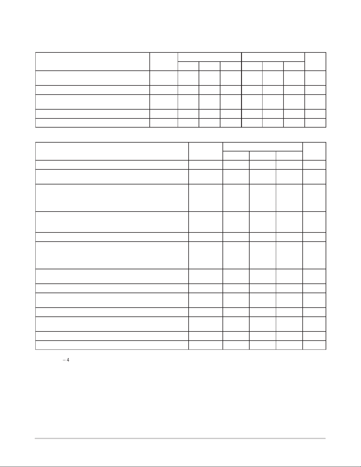
ELECTRICAL CHARACTERISTICS (continued) (V
otherwise noted.)
Characteristic Symbol Min Typ Max Min Typ Max Unit
Output Noise Voltage (TA = 25°C) V
10 Hz ≤ f ≤ 100 kHz
Output Resistance f = 1.0 kHz r
Short Circuit Current Limit (TA = 25°C) I
Vin = 35 Vdc
Peak Output Current (TJ = 25°C) I
Average Temperature Coefficient of Output Voltage TCV
ELECTRICAL CHARACTERISTICS (V
Characteristic Symbol Min Typ Max Unit
Output Voltage (TJ = 25°C) V
Output Voltage (5.0 mA ≤ IO ≤ 1.0 A, PD ≤ 15 W) V
14.8 Vdc ≤ Vin ≤ 27 Vdc
Line Regulation (Note 2.) Reg
14.8 Vdc ≤ Vin ≤ 30 Vdc, IO = 500 mA – 3.8 18
16 Vdc ≤ Vin ≤ 22 Vdc, IO = 1.0 A – 2.2 20
14.5 Vdc ≤ Vin ≤ 27 Vdc, TJ = 25°C – 6.0 120
Load Regulation (Note 2.) Reg
5.0 mA ≤ IO ≤ 1.5 A, TJ = 25°C – – 25
5.0 mA ≤ IO ≤ 1.0 A – – 25
Quiescent Current I
Quiescent Current Change ∆I
15 Vdc ≤ Vin ≤ 30 Vdc, IO = 500 mA – – 0.8
14.8 Vdc ≤ Vin ≤ 27 Vdc, TJ = 25°C – – 0.8
5.0 mA ≤ IO ≤ 1.0 A, TJ = 25°C – – 0.5
Ripple Rejection RR 55 60 – dB
15 Vdc ≤ Vin ≤ 25 Vdc, f = 120 Hz, IO = 500 mA
Dropout Voltage (IO = 1.0 A, TJ = 25°C) VI – V
Output Noise Voltage (TA = 25°C) V
10 Hz ≤ f ≤ 100 kHz
Output Resistance (f = 1.0 kHz) r
Short Circuit Current Limit (TA = 25°C) I
Vin = 35 Vdc
Peak Output Current (TJ = 25°C) I
Average Temperature Coefficient of Output Voltage TCV
1. T
2. Load and line regulation are specified at constant junction temperature. Changes in VO due to heating effects must be taken into account
=0°C for MC78XXAC, C, LM340AT–XX, LM340T–XX T
low
=*40°C for MC78XXB
separately . Pulse testing with low duty cycle is used.
= 19 V, IO = 1.0 A, TJ = T
in
= 19 V, IO = 500 mA, TJ = T
in
MC7812B MC7812C/LM340T–12
n
O
SC
max
O
– 10 – – 10 – µV/V
– 1.1 – – 1.1 – mΩ
– 0.2 – – 0.2 – A
– 2.2 – – 2.2 – A
– –0.8 – – –0.8 – mV/°C
to T
low
high
O
O
line
load
B
B
O
n
O
SC
max
O
= +125°C for MC78XXAC, C, LM340AT–XX, LM340T–XX
high
to T
low
[Note 1.], unless otherwise noted.)
11.75 12 12.25 Vdc
[Note 1.], unless
high
MC7812AC/LM340AT–12
11.5 12 12.5 Vdc
– 3.4 6.0 mA
– 2.0 – Vdc
– 10 – µV/V
– 1.1 – mΩ
– 0.2 – A
– 2.2 – A
– –0.8 – mV/°C
O
mV
mV
mA
O
http://onsemi.com
8
Page 9
MC7800, MC7800A, LM340, LM340A Series
ELECTRICAL CHARACTERISTICS (V
Characteristic Symbol Min Typ Max Min Typ Max Unit
Output Voltage (TJ = 25°C) V
Output Voltage (5.0 mA ≤ IO ≤ 1.0 A, PD ≤ 15 W) V
17.5 Vdc ≤ Vin ≤ 30 Vdc – – – 14.25 15 15.75
18.5 Vdc ≤ Vin ≤ 30 Vdc 14.25 15 15.75 – – –
Line Regulation, TJ = 25°C (Note 2.) Reg
17.9 Vdc ≤ Vin ≤ 30 Vdc – 8.5 300 – 8.5 30
20 Vdc ≤ Vin ≤ 26 Vdc – 3.0 150 – 3.0 28
Load Regulation, TJ = 25°C (Note 2.) Reg
5.0 mA ≤ IO ≤ 1.5 A
Quiescent Current I
Quiescent Current Change ∆I
17.5 Vdc ≤ Vin ≤ 30 Vdc – – – – – 0.8
17.5 Vdc ≤ Vin ≤ 30 Vdc, IO = 1.0 A, TJ = 25°C – – 1.0 – – 0.7
5.0 mA ≤ IO ≤ 1.0 A – – 0.5 – – 0.5
Ripple Rejection RR – 58 – 54 58 – dB
18.5 Vdc ≤ Vin ≤ 28.5 Vdc, f = 120 Hz
Dropout Voltage (IO = 1.0 A, TJ = 25°C) VI – V
Output Noise Voltage (TA = 25°C) V
10 Hz ≤ f ≤ 100 kHz
Output Resistance f = 1.0 kHz r
Short Circuit Current Limit (TA = 25°C) I
Vin = 35 Vdc
Peak Output Current (TJ = 25°C) I
Average Temperature Coefficient of Output Voltage TCV
= 23 V, IO = 500 mA, TJ = T
in
O
O
line
load
B
B
O
n
O
SC
max
O
to T
low
MC7815B MC7815C/LM340T–15
14.4 15 15.6 14.4 15 15.6 Vdc
– 1.8 300 – 1.8 55 mV
– 3.5 8.0 – 3.5 6.5 mA
– 2.0 – – 2.0 – Vdc
– 10 – – 10 – µV/V
– 1.2 – – 1.2 – mΩ
– 0.2 – – 0.2 – A
– 2.2 – – 2.2 – A
– –1.0 – – –1.0 – mV/°C
[Note 1.], unless otherwise noted.)
high
Vdc
mV
mA
O
ELECTRICAL CHARACTERISTICS (V
Characteristic Symbol Min Typ Max Unit
Output Voltage (TJ = 25°C) V
Output Voltage (5.0 mA ≤ IO ≤ 1.0 A, PD ≤ 15 W) V
17.9 Vdc ≤ Vin ≤ 30 Vdc
Line Regulation (Note 2.) Reg
17.9 Vdc ≤ Vin ≤ 30 Vdc, IO = 500 mA – 8.5 20
20 Vdc ≤ Vin ≤ 26 Vdc – 3.0 22
17.5 Vdc ≤ Vin ≤ 30 Vdc, IO = 1.0 A, TJ = 25°C – 7.0 20
Load Regulation (Note 2.) Reg
5.0 mA ≤ IO ≤ 1.5 A, TJ = 25°C – 1.8 25
5.0 mA ≤ IO ≤ 1.0 A – 1.5 25
250 mA ≤ IO ≤ 750 mA – 1.2 15
Quiescent Current I
Quiescent Current Change ∆I
17.5 Vdc ≤ Vin ≤ 30 Vdc, IO = 500 mA – – 0.8
17.5 Vdc ≤ Vin ≤ 30 Vdc, IO = 1.0 A, TJ = 25°C – – 0.8
5.0 mA ≤ IO ≤ 1.0 A – – 0.5
1. T
2. Load and line regulation are specified at constant junction temperature. Changes in VO due to heating effects must be taken into account
=0°C for MC78XXAC, C, LM340AT–XX, LM340T–XX T
low
=*40°C for MC78XXB
separately . Pulse testing with low duty cycle is used.
= 23 V, IO = 1.0 A, TJ = T
in
low
high
to T
[Note 1.], unless otherwise noted.)
high
MC7815AC/LM340AT–15
O
O
line
load
B
B
= +125°C for MC78XXAC, C, LM340AT–XX, LM340T–XX
14.7 15 15.3 Vdc
14.4 15 15.6 Vdc
– 3.5 6.0 mA
mV
mV
mA
http://onsemi.com
9
Page 10
MC7800, MC7800A, LM340, LM340A Series
ELECTRICAL CHARACTERISTICS (continued) (V
otherwise noted.)
Characteristic Symbol Min Typ Max Unit
Ripple Rejection RR 60 80 – dB
18.5 Vdc ≤ Vin ≤ 28.5 Vdc, f = 120 Hz, IO = 500 mA
Dropout Voltage (IO = 1.0 A, TJ = 25°C) VI – V
Output Noise Voltage (TA = 25°C) V
10 Hz ≤ f ≤ 100 kHz
Output Resistance f = 1.0 kHz r
Short Circuit Current Limit (TA = 25°C) I
Vin = 35 Vdc
Peak Output Current (TJ = 25°C) I
Average Temperature Coefficient of Output Voltage TCV
ELECTRICAL CHARACTERISTICS (V
Characteristic Symbol Min Typ Max Min Typ Max Unit
Output Voltage (TJ = 25°C) V
Output Voltage (5.0 mA ≤ IO ≤ 1.0 A, PD ≤ 15 W) V
21 Vdc ≤ Vin ≤ 33 Vdc – – – 17.1 18 18.9
22 Vdc ≤ Vin ≤ 33 Vdc 17.1 18 18.9 – – –
Line Regulation, (Note 2.) Reg
21 Vdc ≤ Vin ≤ 33 Vdc – 9.5 360 – 9.5 50
24 Vdc ≤ Vin ≤ 30 Vdc – 3.2 180 – 3.2 25
Load Regulation, (Note 2.) Reg
5.0 mA ≤ IO ≤ 1.5 A
Quiescent Current I
Quiescent Current Change ∆I
21 Vdc ≤ Vin ≤ 33 Vdc – – – – – 1.0
5.0 mA ≤ IO ≤ 1.0 A – – 0.5 – – 0.5
Ripple Rejection RR – 57 – 53 57 – dB
22 Vdc ≤ Vin ≤ 33 Vdc, f = 120 Hz
Dropout Voltage (IO = 1.0 A, TJ = 25°C) ViI – V
Output Noise Voltage (TA = 25°C) V
10 Hz ≤ f ≤ 100 kHz
Output Resistance f = 1.0 kHz r
Short Circuit Current Limit (TA = 25°C) I
Vin = 35 Vdc
Peak Output Current (TJ = 25°C) I
Average Temperature Coefficient of Output Voltage TCV
1. T
2. Load and line regulation are specified at constant junction temperature. Changes in VO due to heating effects must be taken into account
=0°C for MC78XXAC, C, LM340AT–XX, LM340T–XX T
low
=*40°C for MC78XXB
separately . Pulse testing with low duty cycle is used.
= 27 V, IO = 500 mA, TJ = T
in
= 23 V, IO = 1.0 A, TJ = T
in
SC
max
to T
low
MC7818B MC7818C
O
O
line
load
B
B
n
O
SC
max
17.3 18 18.7 17.3 18 18.7 Vdc
– 2.0 360 – 2.0 55 mV
– 3.5 8.0 – 3.5 6.5 mA
O
O
– 2.0 – – 2.0 – Vdc
– 10 – – 10 – µV/V
– 1.3 – – 1.3 – mΩ
– 0.2 – – 0.2 – A
– 2.2 – – 2.2 – A
– –1.5 – – –1.5 – mV/°C
= +125°C for MC78XXAC, C, LM340AT–XX, LM340T–XX
high
to T
low
O
n
O
O
[Note 1.], unless otherwise noted.)
high
[Note 1.], unless
high
MC7815AC/LM340A T–15
– 2.0 – Vdc
– 10 – µV/V
– 1.2 – mΩ
– 0.2 – A
– 2.2 – A
– –1.0 – mV/°C
O
Vdc
mV
mA
O
http://onsemi.com
10
Page 11
MC7800, MC7800A, LM340, LM340A Series
ELECTRICAL CHARACTERISTICS (V
Characteristic Symbol Min Typ Max Unit
Output Voltage (TJ = 25°C) V
Output Voltage (5.0 mA ≤ IO ≤ 1.0 A, PD ≤ 15 W) V
21 Vdc ≤ Vin ≤ 33 Vdc
Line Regulation (Note 2.) Reg
21 Vdc ≤ Vin ≤ 33 Vdc, IO = 500 mA – 9.5 22
24 Vdc ≤ Vin ≤ 30 Vdc, IO = 1.0 A – 3.2 25
24 Vdc ≤ Vin ≤ 30 Vdc, IO = 1.0 A, TJ = 25°C – 3.2 10.5
20.6 Vdc ≤ Vin ≤ 33 Vdc, IO = 1.0 A, TJ = 25°C – 8.0 22
Load Regulation (Note 2.) Reg
5.0 mA ≤ IO ≤ 1.5 A, TJ = 25°C – 2.0 25
5.0 mA ≤ IO ≤ 1.0 A – 1.8 25
250 mA ≤ IO ≤ 750 mA – 1.5 15
Quiescent Current I
Quiescent Current Change ∆I
21 Vdc ≤ Vin ≤ 33 Vdc, IO = 500 mA – – 0.8
21.5 Vdc ≤ Vin ≤ 30 Vdc, TJ = 25°C – – 0.8
5.0 mA ≤ IO ≤ 1.0 A – – 0.5
Ripple Rejection RR 53 57 – dB
22 Vdc ≤ Vin ≤ 32 Vdc, f = 120 Hz, IO = 500 mA
Dropout Voltage (IO = 1.0 A, TJ = 25°C) VI – V
Output Noise Voltage (TA = 25°C) V
10 Hz ≤ f ≤ 100 kHz
Output Resistance f = 1.0 kHz r
Short Circuit Current Limit (TA = 25°C) I
Vin = 35 Vdc
Peak Output Current (TJ = 25°C) I
Average Temperature Coefficient of Output Voltage TCV
= 27 V, IO = 1.0 A, TJ = T
in
low
to T
[Note 1.], unless otherwise noted.)
high
MC7818AC
O
O
line
load
B
B
O
n
O
SC
max
O
17.64 18 18.36 Vdc
17.3 18 18.7 Vdc
– 3.5 6.0 mA
– 2.0 – Vdc
– 10 – µV/V
– 1.3 – mΩ
– 0.2 – A
– 2.2 – A
– –1.5 – mV/°C
mV
mV
mA
O
ELECTRICAL CHARACTERISTICS (V
Characteristic Symbol Min Typ Max Min Typ Max Unit
Output Voltage (TJ = 25°C) V
Output Voltage (5.0 mA ≤ IO ≤ 1.0 A, PD ≤ 15 W) V
27 Vdc ≤ Vin ≤ 38 Vdc – – – 22.8 24 25.2
28 Vdc ≤ Vin ≤ 38 Vdc 22.8 24 25.2 – – –
Line Regulation, (Note 2.) Reg
27 Vdc ≤ Vin ≤ 38 Vdc – 11.5 480 – 2.7 60
30 Vdc ≤ Vin ≤ 36 Vdc – 3.8 240 – 2.7 48
Load Regulation, (Note 2.) Reg
5.0 mA ≤ IO ≤ 1.5 A
Quiescent Current I
Quiescent Current Change ∆I
27 Vdc ≤ Vin ≤ 38 Vdc – – – – – 1.0
5.0 mA ≤ IO ≤ 1.0 A – – 0.5 – – 0.5
1. T
2. Load and line regulation are specified at constant junction temperature. Changes in VO due to heating effects must be taken into account
=0°C for MC78XXAC, C, LM340AT–XX, LM340T–XX T
low
=*40°C for MC78XXB
separately . Pulse testing with low duty cycle is used.
= 33 V, IO = 500 mA, TJ = T
in
O
O
line
load
B
B
to T
low
MC7824B MC7824C
23 24 25 23 24 25 Vdc
– 2.1 480 – 4.4 65 mV
– 3.6 8.0 – 3.6 6.5 mA
= +125°C for MC78XXAC, C, LM340AT–XX, LM340T–XX
high
[Note 1.], unless otherwise noted.)
high
Vdc
mV
mA
http://onsemi.com
11
Page 12
MC7800, MC7800A, LM340, LM340A Series
ELECTRICAL CHARACTERISTICS (continued) (V
otherwise noted.)
Characteristic Symbol Min Typ Max Min Typ Max Unit
Ripple Rejection RR – 54 – 50 54 – dB
28 Vdc ≤ Vin ≤ 38 Vdc, f = 120 Hz
Dropout Voltage (IO = 1.0 A, TJ = 25°C) VI – V
Output Noise Voltage (TA = 25°C) V
10 Hz ≤ f ≤ 100 kHz
Output Resistance f = 1.0 kHz r
Short Circuit Current Limit (TA = 25°C) I
Vin = 35 Vdc
Peak Output Current (TJ = 25°C) I
Average Temperature Coefficient of Output Voltage TCV
ELECTRICAL CHARACTERISTICS (V
Characteristic Symbol Min Typ Max Unit
Output Voltage (TJ = 25°C) V
Output Voltage (5.0 mA ≤ IO ≤ 1.0 A, PD ≤ 15 W) V
27.3 Vdc ≤ Vin ≤ 38 Vdc
Line Regulation (Note 2.) Reg
27 Vdc ≤ Vin ≤ 38 Vdc, IO = 500 mA – 11.5 25
30 Vdc ≤ Vin ≤ 36 Vdc, IO = 1.0 A – 3.8 28
30 Vdc ≤ Vin ≤ 36 Vdc, TJ = 25°C – 3.8 12
26.7 Vdc ≤ Vin ≤ 38 Vdc, IO = 1.0 A, TJ = 25°C – 10 25
Load Regulation (Note 2.) Reg
5.0 mA ≤ IO ≤ 1.5 A, TJ = 25°C – 2.1 15
5.0 mA ≤ IO ≤ 1.0 A – 2.0 25
250 mA ≤ IO ≤ 750 mA – 1.8 15
Quiescent Current I
Quiescent Current Change ∆I
27.3 Vdc ≤ Vin ≤ 38 Vdc, IO = 500 mA – – 0.8
27 Vdc ≤ Vin ≤ 38 Vdc, TJ = 25°C – – 0.8
5.0 mA ≤ IO ≤ 1.0 A – – 0.5
Ripple Rejection RR 45 54 – dB
28 Vdc ≤ Vin ≤ 38 Vdc, f = 120 Hz, IO = 500 mA
Dropout Voltage (IO = 1.0 A, TJ = 25°C) VI – V
Output Noise Voltage (TA = 25°C) V
10 Hz ≤ f ≤ 100 kHz
Output Resistance (f = 1.0 kHz) r
Short Circuit Current Limit (TA = 25°C) I
Vin = 35 Vdc
Peak Output Current (TJ = 25°C) I
Average Temperature Coefficient of Output Voltage TCV
1. T
2. Load and line regulation are specified at constant junction temperature. Changes in VO due to heating effects must be taken into account
=0°C for MC78XXAC, C, LM340AT–XX, LM340T–XX T
low
=*40°C for MC78XXB
separately . Pulse testing with low duty cycle is used.
= 33 V, IO = 1.0 A, TJ = T
in
= 33 V, IO = 500 mA, TJ = T
in
MC7824B MC7824C
O
n
O
SC
max
O
– 2.0 – – 2.0 – Vdc
– 10 – – 10 – µV/V
– 1.4 – – 1.4 – mΩ
– 0.2 – – 0.2 – A
– 2.2 – – 2.2 – A
– –2.0 – – –2.0 – mV/°C
to T
low
high
O
O
line
load
B
B
O
n
O
SC
max
O
= +125°C for MC78XXAC, C, LM340AT–XX, LM340T–XX
high
to T
low
[Note 1.], unless otherwise noted.)
[Note 1.], unless
high
MC7824AC
23.5 24 24.5 Vdc
23.2 24 25.8 Vdc
– 3.6 6.0 mA
– 2.0 – Vdc
– 10 – µV/V
– 1.4 – mΩ
– 0.2 – A
– 2.2 – A
– –2.0 – mV/°C
O
mV
mV
mA
O
http://onsemi.com
12
Page 13
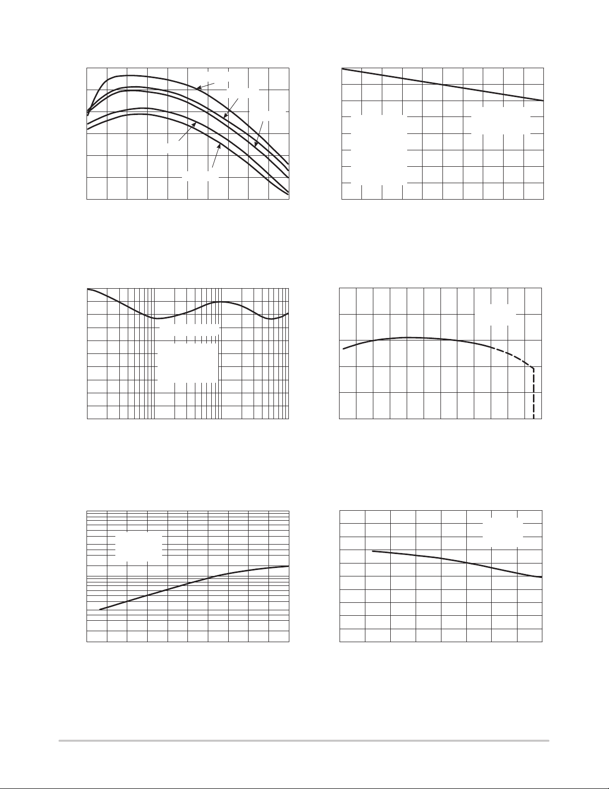
I
3.0
,
OUTPUT
CURR
NT
(A)
80
RR,
RIPPL
R
CTION
(dB)
,
OUTPUT
IMP
DANC
(
)
Z
MC7800, MC7800A, LM340, LM340A Series
TJ = –40°C
2.5
E
2.0
1.5
1.0
O
0.5
0
4.0 8.0 12 20 30 40
6.0 10 15 25 35
Vin–V
out
TJ = 85°C
TJ = 125°C
, INPUT/OUPUT VOLTAGE DIFFERENTIAL (V)
Figure 1. Peak Output Current as a Function of
Input/Output Differential Voltage (MC78XXC, AC, B)
80
TJ = 0°C
TJ = 25°C
70
PART # V
MC7805C = 10 V
60
MC7806C = 11 V
MC7808C = 14 V
RR, RIPPLE REJECTION (dB)
MC7812C = 19 V
MC7815C = 23 V
50
MC7818C = 27 V
MC7824C = 33 V
40
4.0 6.0 8.0 10 12 14 16 18 20 22 24
in
VO, OUTPUT VOLTAGE (V)
f = 120 Hz
IO = 20 mA
∆Vin = 1.0 V(RMS)
Figure 2. Ripple Rejection as a Function of
Output Voltages (MC78XXC, AC, B)
70
MC78XXB, C, AC
EJE
E
60
50
40
30
0.01
Vin = 8.0 V to 18 V
IO = 500 mA
f = 120 Hz
TA = 25°C
0.1 10
f, FREQUENCY (kHz)
1.0
Figure 3. Ripple Rejection as a Function of
Frequency (MC78XXC, AC, B)
10
5.0
Ω
m
E
3.0
2.0
E
1.0
0.5
0.3
O
0.2
0.1
4.0 8.0 12 16 20 24
f = 120 Hz
IO = 500 mA
CL = 0 µF
VO, OUTPUT VOLTAGE (V)
Figure 5. Output Impedance as a Function of
Output Voltage (MC78XXC, AC, B)
5.0
4.9
, OUTPUT VOLTAGE (V)
O
V
4.8
–60 –20 20 60 100 140 180
TJ, JUNCTION TEMPERATURE (°C)
Vin = 20 V
IO = 5.0 mA
Figure 4. Output Voltage as a Function of
Junction Temperature (MC7805C, AC, B)
6.0
Vin = 10 V
VO = 5.0 V
IL = 20 mA
, QUIESCENT CURRENT (mA)
B
I
4.0
3.0
2.0
1.0
0
–75 –50
–25 0 25 50 75 100 125
TJ, JUNCTION TEMPERATURE (°C)
Figure 6. Quiescent Current as a Function of
Temperature (MC78XXC, AC, B)
http://onsemi.com
13
Page 14
MC7800, MC7800A, LM340, LM340A Series
APPLICATIONS INFORMATION
Design Considerations
The MC7800 Series of fixed voltage regulators are
designed with Thermal Overload Protection that shuts down
the circuit when subjected to an excessive power overload
condition, Internal Short Circuit Protection that limits the
maximum current the circuit will pass, and Output Transistor
Safe–Area Compensation that reduces the output short circuit
current as the voltage across the pass transistor is increased.
In many low current applications, compensation
capacitors are not required. However, it is recommended
that the regulator input be bypassed with a capacitor if the
regulator is connected to the power supply filter with long
Input
0.33 µF
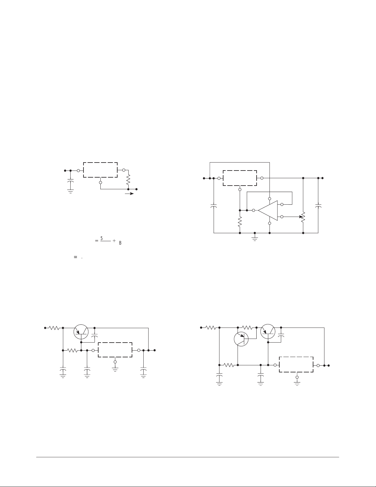
The MC7800 regulators can also be used as a current source when
connected as above. In order to minimize dissipation the MC7805C is
chosen in this application. Resistor R determines the current as follows:
MC7805
R
Constant
Current to
Grounded
Load
I
O
wire lengths, or if the output load capacitance is large. An
input bypass capacitor should be selected to provide good
high–frequency characteristics to insure stable operation
under all load conditions. A 0.33 µF or larger tantalum,
mylar, or other capacitor having low internal impedance at
high frequencies should be chosen. The bypass capacitor
should be mounted with the shortest possible leads directly
across the regulators input terminals. Normally good
construction techniques should be used to minimize ground
loops and lead resistance drops since the regulator has no
external sense lead.
Output
0.1 µF
10 k
Input
0.33 µF
MC7805
1.0 k
7
2
6
4
3
MC1741G
5.0 V
IO+
IB ^ 3.2 mA over line and load changes.
For example, a 1.0 A current source would require R to be a 5.0 Ω,
10 W resistor and the output voltage compliance would be the input
voltage less 7.0 V .
)
I
B
R
Figure 7. Current Regulator Figure 8. Adjustable Output Regulator
R
Source
Input
≥ 10 µF
The MC7800 series can be current boosted with a PNP transistor. The
MJ2955 provides current to 5.0 A. Resistor R in conjunction with the V
of the PNP determines when the pass transistor begins conducting; this
circuit is not short circuit proof. Input/output differential voltage minimum is
increased by VBE of the pass transistor.
MJ2955 or Equiv.
0.33 µF
R
1.0 µF
XX = 2 digits of type number indicating voltage.
MC78XX
Output
1.0 µF
BE
VO = 7.0 V to 20 V
VIN = VO ≥ 2.0 V
The addition of an operational amplifier allows adjustment to higher or
intermediate values while retaining regulation characteristics. The
minimum voltage obtainable with this arrangement is 2.0 V greater than the
regulator voltage.
MJ2955
or Equiv.
R
Source
Input
≥ 10 µF
The circuit of Figure 9 can be modified to provide supply protection against
short circuits by adding a short circuit sense resistor, RSC, and an
additional PNP transistor. The current sensing PNP must be able to handle
the short circuit current of the three–terminal regulator. Therefore, a
four–ampere plastic power transistor is specified.
R
SC
0.33 µF
2N6049
or Equiv.
R
1.0 µF
XX = 2 digits of type number indicating voltage.
MC78XX
Output
Figure 9. Current Boost Regulator Figure 10. Short Circuit Protection
http://onsemi.com
14
Page 15
MC7800, MC7800A, LM340, LM340A Series
,
PO
R
DISSIPATION
(
)
P
2.5
20
16
W
12
8.0
WE
4.0
D
0
–50 –25 0 25 50 75 100 125 150
θHS = 0°C/W
θHS = 5°C/W
θHS = 15°C/W
No Heatsink
TA, AMBIENT TEMPERATURE (°C)
θJC = 5°C/W
θJA = 65°C/W
T
= 150°C
J(max)
, INPUT–OUTPUT VOLTAGE
– VV
in out
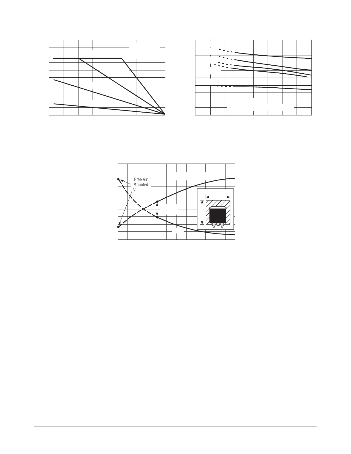
Figure 11. W orst Case Power Dissipation versus
Ambient T emperature (Case 221A)
80
P
Minimum
Size Pad
D(max)
R
θJA
70
60
50
JAθ
JUNCTION-TO-AIR ( C/W)°
40
R , THERMAL RESISTANCE
30
Free Air
Mounted
Vertically
010203025155.0
L, LENGTH OF COPPER (mm)
IO = 1.0 A
IO = 500 mA
2.0
IO = 200 mA
1.5
IO = 20 mA
IO = 0 mA
1.0
DIFFERENTIAL (V)
0.5
0
–75 –50 –25 0 25 50 75 100 125
∆VO = 2% of V
– – – Extended Curve for MC78XXB
TJ, JUNCTION TEMPERATURE (°C)
O
Figure 12. Input Output Differential as a Function
of Junction Temperature (MC78XXC, AC, B)
3.5
for TA = 50°C
2.0 oz. Copper
L
L
3.0
2.5
2.0
1.5
1.0
, MAXIMUM POWER DISSIPATION (W)
D
P
Figure 13. D2P AK Thermal Resistance and Maximum
Power Dissipation versus P.C.B. Copper Length
DEFINITIONS
Line Regulation – The change in output voltage for a
change in the input voltage. The measurement is made under
conditions of low dissipation or by using pulse techniques
such that the average chip temperature is not significantly
affected.
Load Regulation – The change in output voltage for a
change in load current at constant chip temperature.
Maximum Power Dissipation – The maximum total
device dissipation for which the regulator will operate
within specifications.
Quiescent Current – That part of the input current that is
not delivered to the load.
Output Noise V oltage – The rms ac voltage at the output,
with constant load and no input ripple, measured over a
specified frequency range.
Long Term Stability – Output voltage stability under
accelerated life test conditions with the maximum rated
voltage listed in the devices’ electrical characteristics and
maximum power dissipation.
http://onsemi.com
15
Page 16
MC7800, MC7800A, LM340, LM340A Series
T
J
40° to +125°C
T
J
+125°C
6.0 V
T
J
40° to +125°C
T
J
+125°C
8.0 V
T
J
40° to +125°C
TO–220
9.0 V
TO–220
T
J
+125°C
12 V
T
J
40° to +125°C
T
J
+125°C
15 V
T
J
40° to +125°C
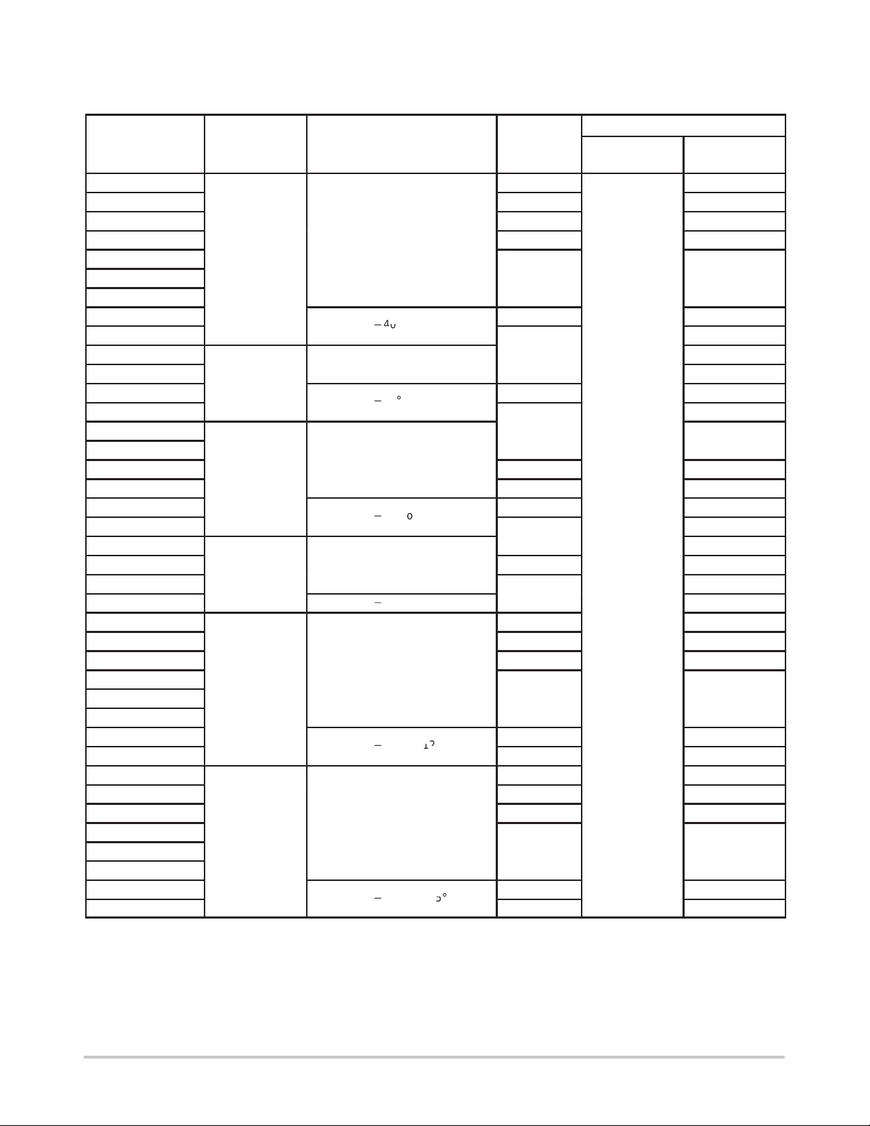
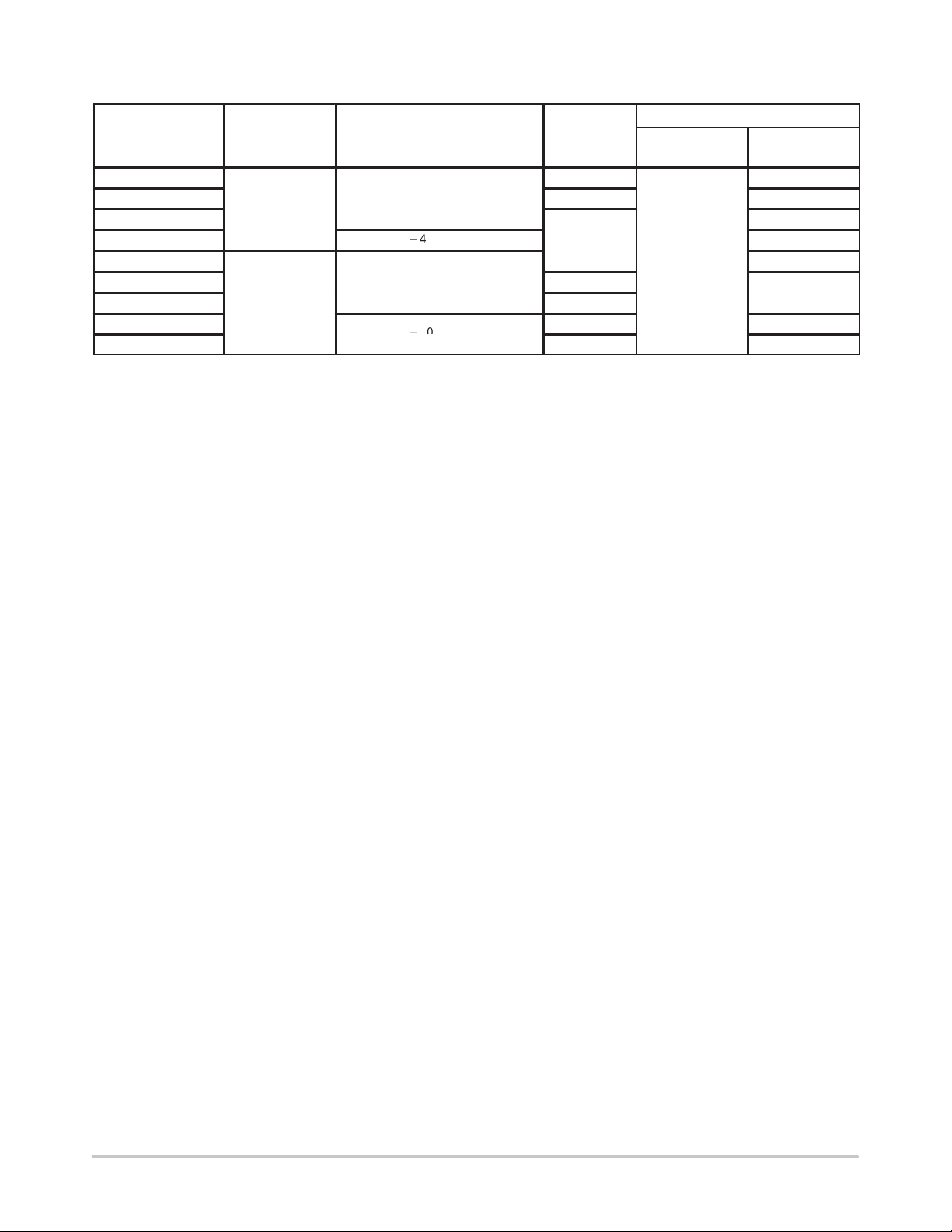
ORDERING INFORMATION
Device Output Voltage Temperature Range Package
MC7805.2CT
MC7805ACD2T/R4
MC7805ACT
MC7805CD2T/R4
MC7805CT
LM340T–5
LM340AT–5
MC7805BD2T/R4
MC7805BT
MC7806ACT
MC7806CT
MC7806BD2T/R4
MC7806BT
MC7808ABT
MC7808ACT
MC7808CD2T/R4
MC7808CT
MC7808BD2T/R4
MC7808BT
MC7809ACT
MC7809CD2T/R4
MC7809CT
MC7809BT
MC7812ACD2T/R4
MC7812ACT
MC7812CD2T/R4
MC7812CT
LM340T–12
LM340AT–12
MC7812BD2T/R4
MC7812BT
MC7815ACD2T/R4
MC7815ACT
MC7815CD2T/R4
MC7815CT
LM340T–15
LM340AT–15
MC7815BD2T/R4
MC7815BT
5.0 V
TJ = 0° to +125°C
*
°
=
*
°
= 0° to
*
°
=
*
°
= 0° to
*
°
=
*
TJ = 0° to +125°C
TJ = *40° to +125°C
°
= 0° to
*
°
=
*
°
= 0° to
*
°
=
*
°
°
°
°
°
°
°
°
°
Shipping
Rails
(No Suffix)
TO–220 –
D2PAK 800 Units/Reel
TO–220 –
D2PAK 800 Units/Reel
TO–220 –
D2PAK 800 Units/Reel
TO–220
D2PAK 800 Units/Reel
TO–220
D2PAK 800 Units/Reel
TO–220 –
D2PAK 800 Units/Reel
50 Units/Rail
D2PAK 800 Units/Reel
D2PAK 800 Units/Reel
TO–220 –
D2PAK 800 Units/Reel
TO–220 –
D2PAK 800 Units/Reel
TO–220 –
D2PAK 800 Units/Reel
TO–220 –
D2PAK 800 Units/Reel
TO–220 –
D2PAK 800 Units/Reel
TO–220 –
Tape & Reel
(R4 Suffix)
–
–
–
–
–
–
–
–
–
http://onsemi.com
16
Page 17
MC7800, MC7800A, LM340, LM340A Series
18 V
T
J
40° to +125°C
ORDERING INFORMATION
Device Output Voltage Temperature Range Package
MC7818ACT
MC7818CD2T/R4
MC7818CT
MC7818BT
MC7824ACT
MC7824CD2T
MC7824CT
MC7824BD2T/R4
MC7824BT
24 V
TJ = 0° to +125°C
TJ = *40° to +125°C
TJ = 0° to +125°C
*
=
°
*
°
Shipping
Rails
(No Suffix)
TO–220 –
D2PAK 800 Units/Reel
TO–220
50 Units/Rail
D2PAK
TO–220
D2PAK 800 Units/Reel
TO–220 –
Tape & Reel
(R4 Suffix)
–
–
–
–
http://onsemi.com
17
Page 18

MC7800, MC7800A, LM340, LM340A Series
MARKING DIAGRAMS
MC7800, MC7800A Series
MC
78xxXXT
ALYWW
78xxXXT
ALYWW
MARKING DIAGRAMS
LM340, LM340A Series
LM
340XT–xx
ALYWW
xx = Voltage Option
XX = Appropriate Suffix Options
A = Assembly Location
L = Wafer Lot
Y = Year
WW = Work Week
http://onsemi.com
18
Page 19
MC7800, MC7800A, LM340, LM340A Series
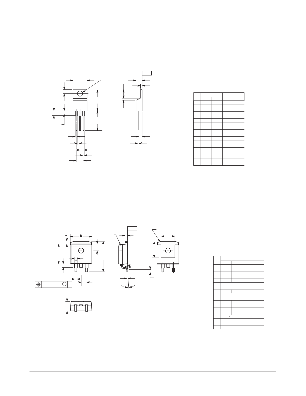
P ACKAGE DIMENSIONS
TO–220
T SUFFIX
CASE 221A–09
ISSUE AA
SEATING
–T–
PLANE
B
4
Q
123
F
T
A
U
C
S
H
K
Z
L
V
R
J
G
D
N
NOTES:
1. DIMENSIONING AND TOLERANCING PER ANSI
Y14.5M, 1982.
2. CONTROLLING DIMENSION: INCH.
3. DIMENSION Z DEFINES A ZONE WHERE ALL
BODY AND LEAD IRREGULARITIES ARE
ALLOWED.
DIM MIN MAX MIN MAX
A 0.570 0.620 14.48 15.75
B 0.380 0.405 9.66 10.28
C 0.160 0.190 4.07 4.82
D 0.025 0.035 0.64 0.88
F 0.142 0.147 3.61 3.73
G 0.095 0.105 2.42 2.66
H 0.110 0.155 2.80 3.93
J 0.018 0.025 0.46 0.64
K 0.500 0.562 12.70 14.27
L 0.045 0.060 1.15 1.52
N 0.190 0.210 4.83 5.33
Q 0.100 0.120 2.54 3.04
R 0.080 0.110 2.04 2.79
S 0.045 0.055 1.15 1.39
T 0.235 0.255 5.97 6.47
U 0.000 0.050 0.00 1.27
V 0.045 ––– 1.15 –––
Z ––– 0.080 ––– 2.04
MILLIMETERSINCHES
D2PAK
D2T SUFFIX
CASE 936–03
ISSUE B
K
B
F
J
D
0.010 (0.254) T
M
C
A
123
G
OPTIONAL
CHAMFER
S
H
NOTES:
1. DIMENSIONING AND TOLERANCING PER ANSI
Y14.5M, 1982.
2. CONTROLLING DIMENSION: INCH.
–T–
E
TERMINAL 4
U
V
M
L
N
P
R
3. TAB CONTOUR OPTIONAL WITHIN DIMENSIONS
A AND K.
4. DIMENSIONS U AND V ESTABLISH A MINIMUM
MOUNTING SURFACE FOR TERMINAL 4.
5. DIMENSIONS A AND B DO NOT INCLUDE MOLD
FLASH OR GATE PROTRUSIONS. MOLD FLASH
AND GATE PROTRUSIONS NOT TO EXCEED
0.025 (0.635) MAXIMUM.
INCHES
DIMAMIN MAX MIN MAX
0.386 0.403 9.804 10.236
B 0.356 0.368 9.042 9.347
C 0.170 0.180 4.318 4.572
D 0.026 0.036 0.660 0.914
E 0.045 0.055 1.143 1.397
F 0.051 REF 1.295 REF
G 0.100 BSC 2.540 BSC
H 0.539 0.579 13.691 14.707
J 0.125 MAX 3.175 MAX
K 0.050 REF 1.270 REF
L 0.000 0.010 0.000 0.254
M 0.088 0.102 2.235 2.591
N 0.018 0.026 0.457 0.660
P 0.058 0.078 1.473 1.981
__
R
S 0.116 REF 2.946 REF
U 0.200 MIN 5.080 MIN
V 0.250 MIN 6.350 MIN
MILLIMETERS
5 REF5 REF
http://onsemi.com
19
Page 20

MC7800, MC7800A, LM340, LM340A Series
ON Semiconductor and are trademarks of Semiconductor Components Industries, LLC (SCILLC). SCILLC reserves the right to make changes
without further notice to any products herein. SCILLC makes no warranty , representation or guarantee regarding the suitability of its products for any particular
purpose, nor does SCILLC assume any liability arising out of the application or use of any product or circuit, and specifically disclaims any and all liability ,
including without limitation special, consequential or incidental damages. “Typical” parameters which may be provided in SCILLC data sheets and/or
specifications can and do vary in different applications and actual performance may vary over time. All operating parameters, including “Typicals” must be
validated for each customer application by customer’s technical experts. SCILLC does not convey any license under its patent rights nor the rights of others.
SCILLC products are not designed, intended, or authorized for use as components in systems intended for surgical implant into the body, or other applications
intended to support or sustain life, or for any other application in which the failure of the SCILLC product could create a situation where personal injury or
death may occur. Should Buyer purchase or use SCILLC products for any such unintended or unauthorized application, Buyer shall indemnify and hold
SCILLC and its officers, employees, subsidiaries, affiliates, and distributors harmless against all claims, costs, damages, and expenses, and reasonable
attorney fees arising out of, directly or indirectly , any claim of personal injury or death associated with such unintended or unauthorized use, even if such claim
alleges that SCILLC was negligent regarding the design or manufacture of the part. SCILLC is an Equal Opportunity/Affirmative Action Employer .
PUBLICATION ORDERING INFORMATION
NORTH AMERICA Literature Fulfillment:
Literature Distribution Center for ON Semiconductor
P.O. Box 5163, Denver, Colorado 80217 USA
Phone: 303–675–2175 or 800–344–3860 Toll Free USA/Canada
Fax: 303–675–2176 or 800–344–3867 Toll Free USA/Canada
Email: [email protected]
Fax Response Line: 303–675–2167 or 800–344–3810 T oll Free USA/Canada
N. American Technical Support: 800–282–9855 Toll Free USA/Canada
EUROPE: LDC for ON Semiconductor – European Support
German Phone : (+1) 303–308–7140 (M–F 1:00pm to 5:00pm Munich T ime)
Email: ONlit–[email protected]
French Phone: (+1) 303–308–7141 (M–F 1:00pm to 5:00pm Toulouse Time)
Email: ONlit–[email protected]
English Phone: (+1) 303–308–7142 (M–F 12:00pm to 5:00pm UK Time)
Email: [email protected]
EUROPEAN TOLL–FREE ACCESS*: 00–800–4422–3781
*Available from Germany, France, Italy, England, Ireland
CENTRAL/SOUTH AMERICA:
Spanish Phone: 303–308–7143 (Mon–Fri 8:00am to 5:00pm MST)
Email: ONlit–[email protected]
ASIA/PACIFIC : LDC for ON Semiconductor – Asia Support
Phone: 303–675–2121 (Tue–Fri 9:00am to 1:00pm, Hong Kong T ime)
T oll Free from Hong Kong & Singapore:
001–800–4422–3781
Email: ONlit–[email protected]
JAPAN: ON Semiconductor, Japan Customer Focus Center
4–32–1 Nishi–Gotanda, Shinagawa–ku, T okyo, Japan 141–8549
Phone: 81–3–5740–2745
Email: [email protected]
ON Semiconductor Website: http://onsemi.com
For additional information, please contact your local
Sales Representative.
http://onsemi.com
20
MC7800/D
 Loading...