

Page 1
For assistance or to order, call (800) 531-5782
78ST300 Series
3 AMP POSITIVE STEP-DOWN
INTEGRATED SWITCHING REGULATOR
Revised 6/30/98
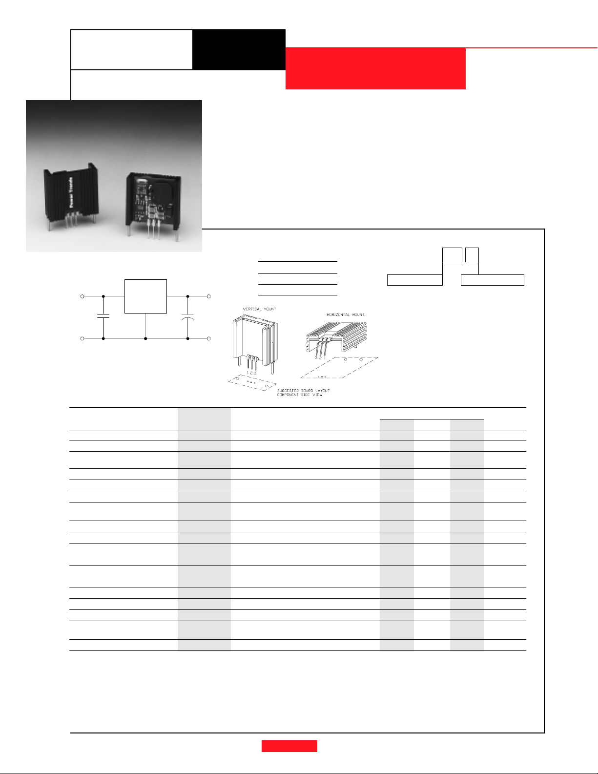
Standard Application
Vin
C1
1
78ST300
C1 = Optional 1µF ceramic
C2 = Required 100µF electrolytic
• High Efficiency > 80%
• Wide Input Range
• Self-Contained Inductor
• Short-Circuit Protection
• Over-Temperature Protection
• Fast Transient Response
The 78ST300 is a series of wide
input voltage, 3 terminal Integrated
Switching Regulators (ISRs). Employing a ceramic substrate, these ISRs
have a maximum output current of 3A.
The output voltage is laser trimmed
for high accuracy.
The 78ST300 series regulators
have internal short-circuit and overtemperature protection and may be
used in a wide variety of applications.
Pin-Out Information
Pin No. Function
1V
in
2 GND
3
2
C2
Vout
+
GNDGND
3V
out
Ordering Information
78ST3 C
Output Voltage
05 = 5.0 Volts
(For dimensions and PC board
layout see Package Style 600.)
Y
XX
Package Suffix
V = Vertical Mount
H = Horizontal
Mount
Specifications
Characteristics
(Ta = 25°C unless noted) Symbols Conditions Min Typ Max Units
Output Current I
Input Voltage Range V
Output Voltage Tolerance ∆V
Line Regulation Reg
Load Regulation Regload 0.1 ≤ Io ≤ 3.0A — ±0.2 ±0.4 %V
Ripple/Noise V
Transient Response t
(with 100µF output cap) Vo over/undershoot 5.0 %V
Efficiency η V
Switching Frequency ƒ
Absolute Maximum T
Operating Temperature Range
Recommended Operating T
Temperature Range Over Vin and Io ranges
Thermal Resistance θ
Storage Temperature T
Mechanical Shock — Per Mil-STD-883D, Method 2002.3 — 500 — G’s
Mechanical Vibration — Per Mil-STD-883D, Method 2007.2,
Weight — — — 11 — Grams
* ISR will operate down to no load with reduced specifications.
** See Thermal Derating chart.
Note:
The 78ST300 Series requires a 100µF electrolytic or tantalum output capacitor for proper operation in all applications.
o
in
o
line
n
tr
o
a
a
ja
s
Over Vin range 0.1* — 3.0 A
Io = 0.1 to 3.0A 8 — 20 V
Over Vin range
Ta = 0°C to +60°C
Over Vin range — ±0.4 ±0.8 %V
Vin = V
min, I
= 3.0A — 1 — %Vo
in
o
50% load change — 100 — µSec
= 9V, Io = 3.0A — 80 — %
in
Over Vin and Io ranges 0.95 1.0 1.05 MHz
— -40 — +70 °C
Free Air Convection, (40-60LFM)
Free Air Convection, (40-60LFM) — 35 — °C/W
— -40 — +125 °C
20-2000 Hz, soldered in a PC board
78ST300 SERIES
— ±1.0 ±2.0 %Vo
-40 — +70** °C
—10—G’s
o
o
o
Power Trends, Inc. 27715 Diehl Road, Warrenville, IL 60555 (800) 531-5782 Fax: (630) 393-6902 http://www.powertrends.com
Page 2
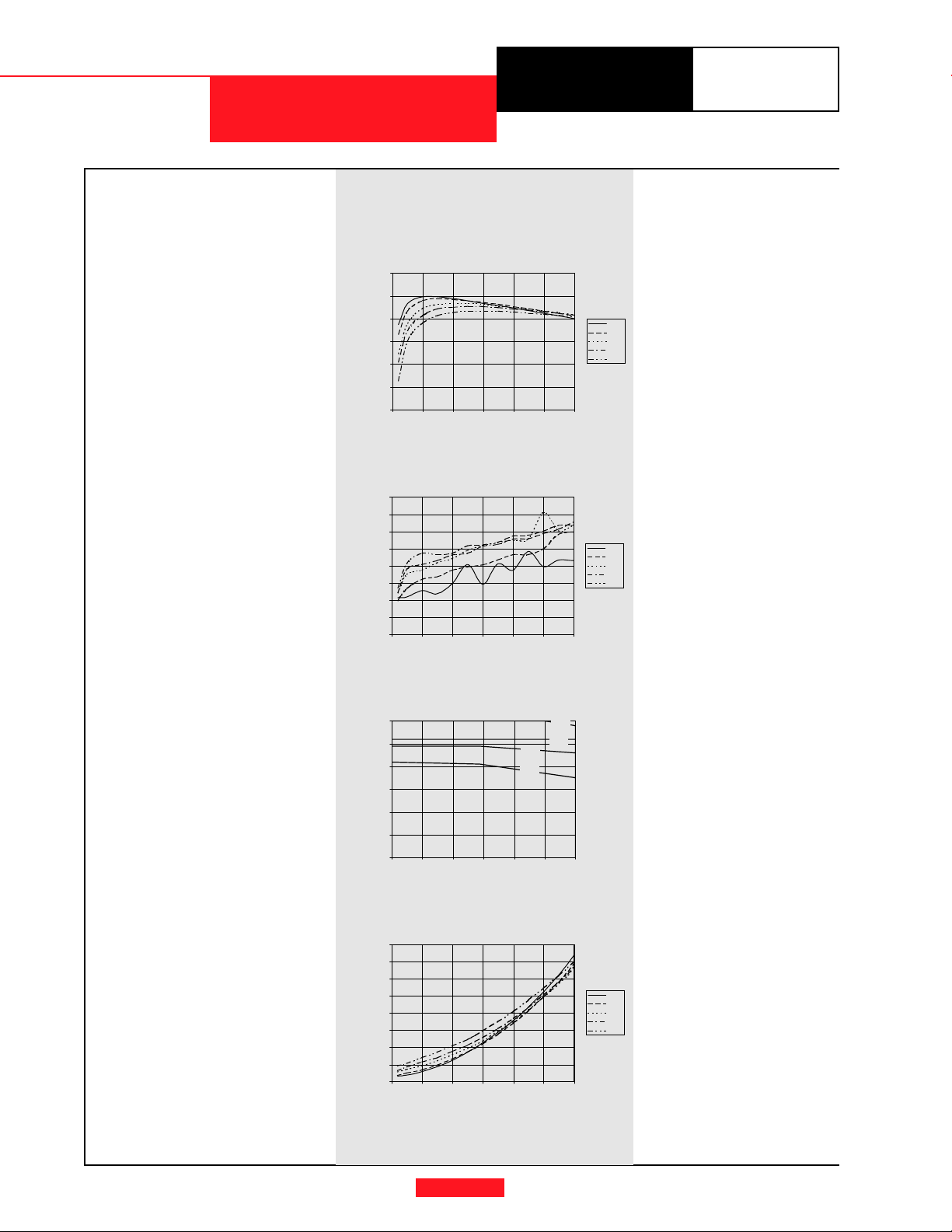
CHARACTERISTIC DATA
78ST305_ 5.0 VDC
(See Note 1)
Efficiency vs Output Current
100
90
80
70
60
Efficiency (%)Ripple (mV)PD (Watts)
50
40
0.00.51.01.52.02.53.0
Iout (A)
Ripple vs Output Current
40
35
30
25
20
15
10
5
0
0.0 0.5 1.0 1.5 2.0 2.5 3.0
Iout (A)
For assistance or to order, call (800) 531-5782
78ST300 Series
Vin
7.5V
9.0V
12.0V
15.0V
20.0V
Vin
7.5V
9.0V
12.0V
15.0V
20.0V
Thermal Derating (Ta) (See Note 2)
3.0
2.5
2.0
1.5
Iout (A)
1.0
0.5
0.0
8 101214161820
Vin (Volts)
70°C
85°C
50°C
60°C
Power Dissipation vs Output Current
4.0
3.5
3.0
2.5
2.0
1.5
1.0
0.5
0.0
0.0 0.5 1.0 1.5 2.0 2.5 3.0
Iout (A)
Note 1: All data listed in the above graphs, except for derating data, has been developed from actual products tested at 25°C. This data is considered typical data for the ISR.
Note 2: Thermal derating graphs are developed in free air convection cooling of 40-60 LFM. (See Thermal Application Note)
Vin
7.5V
9.0V
12.0V
15.0V
20.0V
Power Trends, Inc. 27715 Diehl Road, Warrenville, IL 60555 (800) 531-5782 Fax: (630) 393-6902 http://www.powertrends.com
Page 3

IMPORTANT NOTICE
T exas Instruments and its subsidiaries (TI) reserve the right to make changes to their products or to discontinue
any product or service without notice, and advise customers to obtain the latest version of relevant information
to verify, before placing orders, that information being relied on is current and complete. All products are sold
subject to the terms and conditions of sale supplied at the time of order acknowledgement, including those
pertaining to warranty, patent infringement, and limitation of liability.
TI warrants performance of its semiconductor products to the specifications applicable at the time of sale in
accordance with TI’s standard warranty. Testing and other quality control techniques are utilized to the extent
TI deems necessary to support this warranty . Specific testing of all parameters of each device is not necessarily
performed, except those mandated by government requirements.
CERTAIN APPLICATIONS USING SEMICONDUCTOR PRODUCTS MAY INVOL VE POTENTIAL RISKS OF
DEATH, PERSONAL INJURY, OR SEVERE PROPERTY OR ENVIRONMENTAL DAMAGE (“CRITICAL
APPLICATIONS”). TI SEMICONDUCTOR PRODUCTS ARE NOT DESIGNED, AUTHORIZED, OR
WARRANTED TO BE SUITABLE FOR USE IN LIFE-SUPPORT DEVICES OR SYSTEMS OR OTHER
CRITICAL APPLICA TIONS. INCLUSION OF TI PRODUCTS IN SUCH APPLICATIONS IS UNDERST OOD TO
BE FULLY AT THE CUSTOMER’S RISK.
In order to minimize risks associated with the customer’s applications, adequate design and operating
safeguards must be provided by the customer to minimize inherent or procedural hazards.
TI assumes no liability for applications assistance or customer product design. TI does not warrant or represent
that any license, either express or implied, is granted under any patent right, copyright, mask work right, or other
intellectual property right of TI covering or relating to any combination, machine, or process in which such
semiconductor products or services might be or are used. TI’s publication of information regarding any third
party’s products or services does not constitute TI’s approval, warranty or endorsement thereof.
Copyright 1999, Texas Instruments Incorporated
 Loading...