

78Q2132
1/10BASE-T
HomePNA/Ethernet Transceiver
Advanced Information
Target Specification
August 2000
DESCRIPTION
The 78Q2132 is a 1/10 Ethernet transceiver. This
dual speed transceiver interfaces to a 1Mbps Home
LAN and a 10BASE-T network. The Home LAN
interface is fully Home Phoneline Networking Alliance
(HomePNA) compliant extending Ethernet over
POTS. The HomePNA interface includes the pulse
encoder and decoder plus transmit and receive line
interface filters. Only a telco transformer and external
protection devices are required to complete the
interface. The 78Q2132 also integrates MII and
General Purpose Serial Interface (GPSI) MAC
interfaces. The 10BASE-T Ethernet channel includes
Manchester ENDEC and transmitter with an on-chip
pulse-shaper and a low-power line driver. The
10BASE-T transceiver interfaces to Category-3
unshielded twisted pair (Cat-3 UTP) cabling. The
HomePNA port is connected to the line via a
HomePNA compatible 1:1 transformer having a
series capacitor in the line side and the Ethernet port
is connected to the line via 1:1 (Rx) and 1.414:1 (Tx)
isolation transformers. No external filtering is
required. Communication to the MAC is accomplished
through an IEEE-802.3 compliant media independent
interface (MII) or GPSI. The product is designed for
high performance and low power operation, and can
operate from a single 3.3 V or 5 V supply.
FEATURES
• 1M8 Home LAN interface over POTS
• HomePNA 1.1 compliant
• Integrated HomePNA interface and line filters
• Simultaneous Spectral Compatibility with
Voice, Fax, ISDN, xDSL, Cable Modem with
HomePNA
• 10BASE-T IEEE-802.3 compliant TX and RX
functions requiring only a dual isolation
transformer interface to the line
• Integrated MII, GPSI and 10BASE-T ENDEC
• Full duplex operation capable in 10BASE-T
• Automatic polarity correction for 10BASE-T
signal reception
• Power-saving and power-down modes
including transmitter disable
• Operates with a single 3.3V or 5V supply
• LINK, TX, RX, COL, 10, 1, FDX/SPD, PWR
LED indicators
• User programmable Interrupt pin
• General Purpose I/O Interface
• 80-Lead or 64-Lead TQFP package
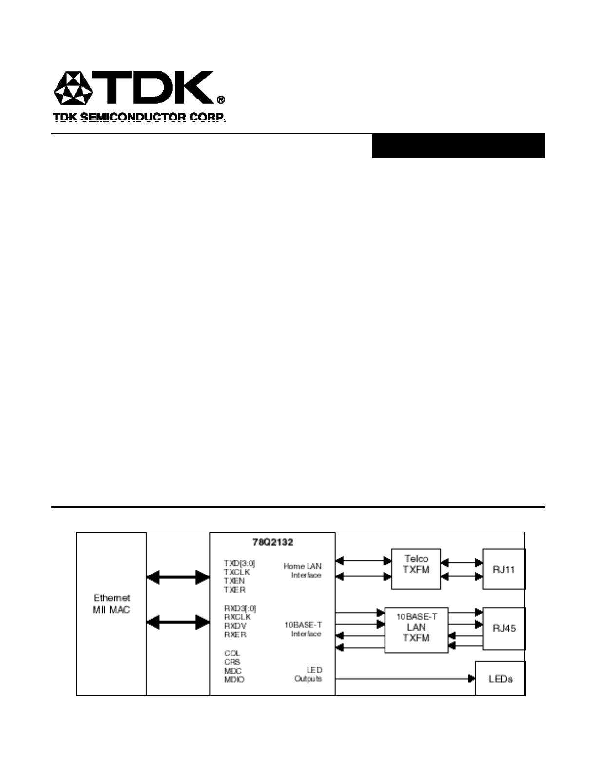
TYPICAL APPLICATION DIAGRAM

78Q2132
1/10BASE-TX
HomePNA/Ethernet Transceiver
FUNCTIONAL DESCRIPTION
GENERAL
Supply Voltage
The 78Q2132 can operate from either a single 3.3V
(± 0.3V) or 5.0V (± 0.5V) power supply. The chip
automatically adapts to the supply voltage used. No
pin configuration is required.
Power Management
Chip power-down is activated by setting the PWRDN
bit in the MII register (MR0.11) or pulling high the
PWRDN pin. When the chip is in power-down
mode, all on-chip circuitry is shut off, and the device
consumes minimum power. While in power-down
state, the 78Q2132 still responds to the
management transactions.
Analog Biasing
The 78Q2132 uses the onchip bandgap and an
external resistor to generate accurate bias voltages
and currents for the circuitry.
Clock Input
The 78Q2132 can use the on-chip crystal oscillator. In
this mode a 25MHz crystal is connected between the
XTAL_IN and XTAL_OUT pins. Alternatively, an
externally generated 25MHz clock can be connected
to the XTAL_IN pin. In conjunction with the oscillator
the device uses a PLLOSC to generate 60MHz which
is divided down by 3 to create 20MHz. It is further
divided for use by various functions on the chip. The
HomePNA section uses the time unit, TIC defined as
60MHz/7 (approx. 116.6ns).
HOMEPNA OPERATION
HomePNA Transmit
The 78Q2132 contains all of the necessary pulse
waveform circuitry to convert the transmit signaling
from a MAC to a HomePNA compliant data-stream.
The conversion is from either a 4bit parallel data
word via the MII interface or the serial data-stream
from GPSI interface to a serial data stream to a
RLL25 encoded set of 3 to 6bits. The value created,
between 0 and 24, is used to modulate the time, in
TIC increments, between pulse bursts. The pulse
bursts are filtered to bandlimit the signal passed to
the line driver, and to the line for transmission. The
integrated envelop-shaper reduces out-of-band
energy to reduce interference. The line driver
requires an external 1:1 isolation transformer to
interface with the line media. Only an external
transient protector and a couple of EMI suppression
inductors are required with the transformer. Note
the transformer requires a coupling capacitor on the
line side.
The 78Q2132 conforms to the required envelope for
transmission bursts on the line. See Figure 6 for the
detail of a single pulse burst signal.
The output is fed to a bandpass filter to reduce out-ofband components. When not transmitting the transmit
circuitry is put into a mode that rejects common-mode
signals appearing at the receiver input.
HomePNA Receive
The 78Q2132 receives the encoded digital signal
through the same 1:1 transformer used for
transmission. The signal is internally filtered and
compared to an adjusted noise threshold prior to
being decoded. From the resulting signal and
internal time reference a value is assigned to the
time interval. The value is RLL25 decoded and the
bit-stream is presented to the serial to parallel
converter. The parallel data from the converter is
then aligned and mapped as a 4 bit data for the MII
as outlined in Table 24-1 in Clause 24 of IEEE-802.3
or sent to the serial GSPI interface.
The receive channel consists of a prefilter,
AGC/main filter, FWR, LPF and comparator with
adjustable level. Following the prefilter is a 2-level
AGC that compresses the dynamic range
requirements of the signal prior to going through the
main HomePNA receive filter.
Natural Loopback
When the 78Q2132 is transmitting on the twisted
pair media, data on the TXD pins is looped back
onto the RXD pins. The natural loopback function
can be disabled through register bit MR16.10.
REFERENCE PACKET FRAMING AND
SEQUENCE
The frame passed between the MAC and 1M8 PHY
on TX-DATA and RX-DATA conforms to the 802.3
Ethernet MAC frame. When a pulse begins
transmission, the previous Symbol interval ends and
a new one immediately begins.
The Run Length Limit (RLL25) code was developed
for the 1M8 PHY. It produces both the highest bit
rate for a given value of Inter Symbol Blanking
Interval (ISBI) and Time Interval Clock (TIC) size. In
a manner similar to run length limited disk coding,
RLL25 encodes data bits in groups of varying sizes,
2

78Q2132
1/10BASE-TX
HomePNA/Ethernet Transceiver
specifically, 3,4,5 and 6 bits. Pulse positions are
assigned to the encoded bit groups in a manner that
causes more data bits to be encoded in positions
that are farther apart. This keeps both the average
and minimum bit rates higher.
HomePNA 1.1 Compatibility
MR19.11 will reflect the version of HomePNA to be
utilized to set the Link Status bit MR1.2. When
MR19.11 is a logic zero, the device will behave as a
HomePNA v1.0 compliant PHY. This will result in
the Link Status bit MR1.2 always being logic one. If
MR19.11 is set to logic one, the device will behave
as a HomePNA 1.1 compliant PHY.
To enable link integrity checking as specified by
HomePNA v1.1, the PHY continually checks for
packet reception. Upon a lapse of packets greater
than 4seconds, the link status bit, MR1.2, is cleared.
Also, for HomePNA v1.1 compatibility, the PHY can
be commanded to place a RUNT or MINIMUM
packet out at any time. These packets, along with
normal packets, indicate to other transceivers that
the link is up when sent at least every 2seconds.
10BASE-T OPERATION
10BASE-T Transmit
The 78Q2132 takes 4 bit parallel NRZ data via the
MII interface and passes it through a parallel to
serial converter. The data is then passed through a
Manchester encoder and then on to the twisted pair
pulse shaping circuitry and the twisted pair drive
circuitry. An advanced pulse shaper employs a GmC filter to pre-distort the output waveform to meet the
output voltage template and spectral content
requirements detailed in Clause 14 of IEEE-802.3.
Interface to the twisted pair media is through a
center-tapped 1.414:1 transformer with 100 ohm
load resistors; no external filtering is required.
During 10BASE-T idle periods, normal link pulses
(NLP) are transmitted. During auto-negotiation of
half or full duplex, fast link pulses (FLP) are
transmitted. When neither data nor link pulses are
being transmitted, the bias current to the transmitter
is cut to 1% of normal. This reduces the power
consumption during idle periods.
The 78Q2132 employs an onboard timer to prevent
the MAC from capturing a network through
excessively long transmissions. When this timer is
exceeded the chip enters the Jabber State, and
transmission is disabled. The jabber state is exited
after the MII goes idle for 500ms ± 250ms.
10BASE-T Receive
The 78Q2132 receives Manchester encoded
10BASE-T data through the twisted pair inputs and
re-establishes logic levels through a slicer with a
smart squelch function. The slicer automatically
adjusts its level after valid data with the appropriate
levels are detected. Data is passed on to the
10BASE-T PLL where the clock is recovered, data is
re-timed and passed through a Manchester decoder.
From here data enters the serial to parallel converter
for transmission to the MAC via the media
independent interface. Interface to the twisted pair
media is through an external 100 ohm resistor and a
1:1 center-tapped transformer; no external filtering is
required. Polarity information is detected and
corrected in the internal circuitry.
Receive Signal
The integrated signal qualifier has separate squelch and
un-squelch thresholds, and includes a built-in timer to
ensure fast and accurate signal detection and receive
noise rejection. Upon detection of two or more valid
10BASE-T pulses on the line receive port, the pass
indication, indicating the presence of valid receive signals
or data, will be asserted. When pass is asserted, the
signal detect threshold is lowered by about 60%, and all
adaptive circuits are released from their quiescent
operating conditions, allowing them to lock onto the
incoming data. In 10BASE-T operation, pass will be deasserted whenever no Manchester data is received. In
either case, the signal detect threshold will return to the
squelched level whenever the pass indication is deasserted. The pass signal is used internally to control the
operation of the receive clock recovery.
Receive Clock Recovery
In 10BASE-T mode, the 10MHz clock is recovered
using a PLL. For fast acquisition, the receive PLL is
locked onto the transmit reference clock during idle
receive periods. When Manchester-coded preambles
are detected, the PLL adjusts its phase and resynchronizes with the incoming Manchester data.
Polarity Correction
The 78Q2132 is capable of either automatic or
manual polarity reversal for 10BASE-T and autonegotiation. Register bits MR16.5 and MR16.4
control these features. The default is automatic
mode where MR16.5 is low and MR16.4 indicates if
the detection circuitry has inverted the input signal.
To enter manual mode, MR16.5 is set high and
MR16.4 will then control the signal polarity.
3

78Q2132
µ
1/10BASE-TX
HomePNA/Ethernet Transceiver
SQE Test
The 78Q2132 supports the signal quality error (SQE)
function detailed in IEEE-802.3. At an interval of 1
s after each negative transition of the TXEN pin in
10BASE-T mode, the COL pin will go high for a
period of 1µs. This function can be disabled through
register bit MR16.11.
Natural Loopback
When the 78Q2132 is transmitting and not receiving
on the twisted pair media, data on the TXD pins is
looped back onto the RXD pins. During a collision,
signal from the analog receive pins is decoded and
sent to the digital RXD pins, as normal. The natural
loopback function can be enabled through register
bit MR16.10.
Auto-Negotiation
The 78Q2132 supports the auto-negotiation function
of Clause 28 of IEEE-802.3 for 10BASE-T half and
full duplex technologies. This function can be
enabled via a pin strap to the device or through
registers. If the ANEGA pin is tied high, the autonegotiation function defaults to on and bit MR0.12,
ANEGEN, is high after reset. Software can disable
the auto-negotiation function by writing to bit
MR0.12. If the ANEGA pin is tied low the function
defaults to off and bit MR0.12 is set low after reset
and cannot be written.
The contents of MII Register MR4 are sent to the link
partner during auto-negotiation encoded in FLPs.
Technology ability bits MR4.9: 7 are not supported
and are permanently tied low. Bits MR4.6:5 reflect
the state of the TECH[2:0] pins.
After reset, software can disable the bits but they
cannot be enabled unless it’s corresponding
technology is permitted by the TECH pins.
With auto-negotiation enabled the 78Q2132 will start
sending FLPs at power-up, loss of link or a
command to restart, if the HomePNA mode is not
selected. At the same time it will look for either
10BASE-T idle or FLPs from its link partner. If
10BASE-T idle pattern is detected, the 78Q2132
realizes that its link partner is not capable of autonegotiation, falls into parallel detect mode and
configures itself to half-duplex mode. If FLPs are
detected, it decodes and analyzes the link code
word (LCW) transmitted by the link partner. When
three identical LCWs are received (ignoring the
acknowledge bit) the LCW is stored in register 5.
Upon receiving three more identical LCWs, with the
acknowledge bit set, the 78Q2132 configures itself
to either full duplex or half duplex, which ever is
common to the two link partners with Full Duplex
taking priority.
Once auto-negotiation is complete, register bit
MR18.10 will reflect the duplex mode that was
chosen. If HomePNA mode is selected, autonegotiation is disabled and this bit has no meaning.
If auto-negotiation fails to establish a link for any
reason, register bit MR18.12 will reflect this and
auto-negotiation will restart from the beginning.
Writing a one to bit MR0.9, RANEG, will also cause
auto-negotiation to restart.
MEDIA INDEPENDENT INTERFACE
MII Transmit and Receive Operation
The MII interface on the 78Q2132 provides
independent transmit and receive paths for the
1Mb/s HomePNA interface and the 10Mb/s 10BASET data rate as described in Clause 22 of the IEEE-
802.3 standard.
The transmit clock, TX_CLK, provides the timing
reference for the transfer of TX_EN, and TXD[3:0],
signals from the MAC to the 78Q2132. TXD[3:0] is
captured on the rising edge of TX_CLK when
TX_EN is asserted.
The receive clock, RX_CLK, provides the timing
reference to transfer RX_DV, and RXD[3:0], signals
from the 78Q2132 to the MAC. RX_DV transitions
synchronously with respect to RX_CLK and is
asserted when the 78Q2132 is presenting valid data
on RXD[3:0].
General Purpose Serial Interface
The seven signals which comprise the GPSI are
TX_CLK, TX_EN, TX_DATA, RX_CLK, RX_DATA,
CRS, and CLSN. Of these, only TX_EN and
TX_DATA are inputs to the 2132; the other five are
outputs from the 2132.
The transmit clock, TX_CLK, provides the timing
reference for the transfer of TX_EN and TX_DATA
signals from the MAC to the 2132. TX_DATA is
captured on the rising edge of TX_CLK when
TX_EN is asserted.
The receive clock, RX_CLK, provides the timing
reference to transfer the RX_DATA signal from the
2132 to the MAC. RX_DATA transitions
synchronously on the rising edge of RX_CLK.
4

78Q2132
1/10BASE-TX
HomePNA/Ethernet Transceiver
Carrier Sense, CRS, is asserted high whenever a
non-idle condition exists on either the receiver or the
transmitter. Typically, GPSI MACs will ignore CRS
during transmit modes.
The Collision signal, CLSN, indicates a collision has
been detected by the 2132 on the wiring network.
MII/GPSI Selection
The MII on the 78Q2132 is internally connected to
the transmit and receive paths for either the 1M8
HomePNA or the 10BASE-T interface as described
in Clause 22 of the IEEE 802.3 standard. The
MII_EN pin selects the choice of interface or MII
Enable bit MR16.1. If the HomePNA port is enabled
the MII_EN pin or MII_Enable bit can select either
the MII or GPSI Interface. If the device is in
10BASE-T operation both the MII_EN pin and MII
Enable bit will have no effect on the selection
between MII and GPSI.
Station Management Interface
The station management interface consists of
circuitry which implements the serial protocol as
described in Clause 22.2.4.4 of IEEE-802.3. A 16-bit
shift register receives serial data applied to the
MDIO pin at the rising edge of the MDC clock signal.
Once the preamble is received, the station
management control logic looks for the start-offrame sequence and a read or write op-code,
followed by the PHYAD and REGAD fields. For a
read operation, the MDIO port becomes enabled as
an output and the register data is loaded into a shift
register for transmission. The 78Q2132 can work
with a one-bit preamble rather than the 32 bits
prescribed by IEEE-802.3. This allows for faster
programming of the registers. If a register does not
exist at an address indicated by the REGAD field or
if the PHYAD field does not match the 78Q2132
PHYAD indicated by the PHYAD pins, a read of the
MDIO port will return all ones. For a write operation,
the data is shifted in and loaded into the appropriate
register after the sixteenth data bit has been
received. Writes to registers not supported by the
78Q2132 are ignored.
When the PHYAD field is all zeros, the Station
Management Entity (STA) is requesting a broadcast
data transaction. All PHYs sharing the same
Management Interface must respond to this
broadcast request. The 78Q2132 responds to the
broadcast data transaction.
ADDITIONAL FEATURES
LED Indicators
There are eight LED pins that can be used to
indicate various states of operation of the 2132.
There are LED pins that indicate when the 2132 is
either transmitting LEDTX or receiving LEDRX, one
that signals a collision event LEDCOL, two more that
reflect the data rate LED1 and LED10. LFD_SPD
reflects full duplex mode of operation when in 802.3
mode and transmit speed when in HomePNA mode.
LEDL indicates the link is up in either mode. The
LEDPWR pin indicates the power level of the
HomePNA port.
General Purpose I/O Interface
The 78Q2132 has a two pin, bi-directional, general
purpose interface that can be used for external
control or to monitor external signals. The direction
of these pins and the data that is either driven or
read from these pins is configured via bits MR16.9:6
as detailed in the Vendor Specific Register
description in MR16.
Interrupt Pin
The 78Q2132 has an Interrupt pin (INTR) that is
asserted whenever any of the Twenty Four interrupt
bits of MR17.7:0 for 10BASE-T and P1R3 15:0 for
HomePNA are set. These interrupt bits can be
disabled via MR17.15:8 and MR19.12 Interrupt
Enable bits. The Interrupt Level bit, MR16.14,
controls the active level of the INTR pin. When the
INTR pin is not asserted, the pin is held in a high
impedance state.
5

78Q2132
1/10BASE-TX
HomePNA/Ethernet Transceiver
PIN DESCRIPTION
LEGEND
TYPE DESCRIPTION TYPE DESCRIPTION
A Analog Pin I Digital Input
O Digital Output I/O Digital Bi-directional Pin
S Supply OZ Tri-stateable digital output
MII (MEDIA INDEPENDENT INTERFACE)/ GPSI (GENERAL PURPOSE SERIAL INTERFACE)
PIN 80-PIN 64-PIN TYPE DESCRIPTION
TX_CLK
(GPSI & MII)
TX_EN
(GPSI & MII)
TXD[3:0]
(TXD[0] = TXDAT
in GPSI mode)
TX_ER 32 26 I RESERVED
CRS
(GPSI & MII)
COL
(CLSN in GPSI
mode)
RX_CLK
(GPSI & MII)
RX_DV 29 23 OZ
RXD[3:0]
(RXD[0] = RXDAT
in GPSI mode)
RX_ER 31 25 OZ RESERVED
33 27 OZ TRANSMIT CLOCK: TX_CLK is a continuous clock which
provides a timing reference for the TX_EN, TX_ER and TXD[3:0]
signals from the MAC. The clock frequency is 2.5MHz in 10baseT
mode and bursty in HomeLAN mode. When the GPSI port is
selected, this is the transmit clock for the General Purpose Serial
Interface. This pin is tri-stated in isolate mode.
34 28 I
40-37 32-29 I TRANSMIT DATA : When the MII port is selected via the MII_EN
42 34 OZ
41 33 OZ
30 24 OZ RECEIVE CLOCK: RX_CLK is a continuous clock which
23-26 19-22 OZ
TRANSMIT ENABLE : TX_EN is asserted by the MAC to indicate
that valid data for transmission is present on the TXD[3:0] pins.
This pin is shared for both the GPSI interface and the MII interface.
select pin, TXD[3:0] receives data from the MAC for transmission on
a nibble basis. This data is captured on the rising edge of TX_CLK
when TX_EN is high. When the GPSI port is selected, TXD[0] is
used for the serial transmit data, TXDAT.
CARRIER SENSE: CRS is high whenever a non-idle condition
exists on either the transmitter or the receiver. When the GPSI port
is selected, this pin becomes the CRS pin of the GPSI. This pin is
tri-stated in isolate mode.
COLLISION: : When the MII port is selected via the GPSI/MII select
pin, COL is asserted high when a collision has been detected on the
media. In 802.3 mode COL is also used for the SQE test function.
When the GPSI port is selected, this pin becomes the CLSN pin of
the GPSI. This pin is tri-stated in isolate mode.
provides a timing reference to the MAC for the RX_DV, RX_ER
and RXD[3:0] signals. When the GPSI port is selected, this pin
becomes the RX_CLK pin of the GPSI. The clock frequency is
2.5MHz in 10baseT mode and bursty in HomeLAN mode. This
pin is tri-stated in isolate mode.
RECEIVE DATA VALID: RX_DV is asserted high to indicate that
valid data is present on the RXD[3:0] pins. It transitions high
when the start-of-frame delimiter (SFD) is detected. This pin is
tri-stated in isolate mode.
RECEIVE DATA: When the MII port is selected via the MII_EN
select pin, received data is provided to the MAC via RXD[3:0].
When the GPSI port is selected, RXD[0] is used for the serial
received data, RXDAT. This pin is tri-stated in isolate mode.
6

78Q2132
1/10BASE-TX
HomePNA/Ethernet Transceiver
MII (continued)
PIN 80-PIN 64-PIN TYPE DESCRIPTION
MDC 22 18 I MANAGEMENT DATA CLOCK: MDC is the clock used for
transferring data via the MDIO pin.
MDIO 21 17 I/O MANAGEMENT DATA INPUT/OUTPUT: MDIO is a bi-
directional port used to access management registers within the
78Q2132. This pin requires an external pull-up resistor as
specified in IEEE-802.3.
PHYAD[4:0] 14-18 12-16 I PHY ADDRESS: Allows 31 configurable PHY addresses. The
78Q2132 always responds to data transactions via the MII
interface when the PHYAD bits are all zero independent of the
logic levels of the PHYAD pins.
CONTROL AND STATUS
NAME 80-PIN 64-PIN TYPE DESCRIPTION
RST 6 4 I
PWRDN 7 5 I
ISO 57 N/A I
ISODEF 58 N/A I ISOLATE DEFAULT: This pin determines the power-up/reset
ANEGA 66 54 I
RESET: When pulled low the pin resets the chip. There are 3
other ways to reset the chip:
i) through the internal power-on-reset (activated when
the chip is being powered up)
ii) through the MII register bit MR 0.15
iii) upon exiting power-down mode
Refer to the Reset Modes section for more details.
POWER-DOWN: The 2132 may be placed in a low power
consumption state by setting this signal to logic high. While in
power-down state, the 2132 still responds to management
transactions. The same power-down state can also be achieved
through the PWRDN bit in the MII register MR0.11.
ISOLATE: When set to logic one, the 2132 will present a high
impedance on its MII output pins. This allows for multiple PHYs to be
attached to the same MII interface. When the 2132 is isolated, it still
responds to management transactions. The same high impedance
state can also be achieved through the ISO bit in the MII register
MR0.10. This pin also sets the default of the ISO bit.
default of the ISO bit, MR0.10. If it is connected to VDD, ISO
bit will have a default value of 1. If it is connected to GND, ISO
bit will have a default value of 0.
AUTO-NEGOTIATION ABILITY: Strapped to logic high to allow
auto-negotiation function. When strapped to logic low, autonegotiation logic is disabled and manual technology selection
is done through TECH[2:0]. This pin is reflected as ANEGA bit
MR1.3.
7

78Q2132
1/10BASE-TX
HomePNA/Ethernet Transceiver
CONTROL AND STATUS (continued)
NAME 80-PIN 64-PIN TYPE DESCRIPTION
TECH[2:0] 63-65 51-53 I TECHNOLOGY ABILITY/SELECT: TECH[2:0] sets the
technology ability of the chip which is reflected in MR0.13,8,
MR1.14:11 and MR4.12:5.
Mode Function
000 10BaseT, half-duplex, full-duplex
001 10BaseT, half-duplex
010 Reserved
011 10BaseT, half-duplex
100 HomePNA
101 10BaseT, full-duplex
110 Reserved
111 10BaseT, half-duplex, full-duplex, HomePNA
MII_EN 74 60 I
MII ENABLE: When this pin is high, the MII port mode is
selected. When low, its meaning is dependent on the mode of
the chip as shown below:
Mode Function
Hi Lo
HomePNA MII GPSI
10BT MII MII
MDI (Media Dependent Interface )
NAME 80-PIN 64-PIN TYPE DESCRIPTION
802OP, 802ON 3, 5 1, 3 A TRANSMIT OUTPUT POSITIVE/NEGATIVE: Transmitter
outputs for 803.2.
802IP, 802IN 62, 61 50, 49 A RECEIVE INPUT POSITIVE/NEGATIVE: Receiver inputs for
802.3.
NAME 80-PIN 64-PIN TYPE DESCRIPTION
HLIP, HLIN 68, 67 56, 55 A RECEIVE POSITIVE/NEGATIVE: Receiver inputs for
HomePNA
HLOP, HLON 78, 80 62, 64 A TRANSMIT POSITIVE/NEGATIVE: Transmitter outputs for
HomePNA.
8

78Q2132
1/10BASE-TX
HomePNA/Ethernet Transceiver
LED INDICATORS
The LED pins use standard logic drivers. They output a logic low when the LED is meant to be on and a logic high
when it is meant to be off. The LED should be connected in series with a resistor between the output pin and the
power supply.
NAME 80-PIN 64-PIN TYPE DESCRIPTION
LEDL
LEDTX 50 42 O
LEDRX 49 41 O
LEDCOL 48 40 O
LEDPWR 47 39 O LED POWER: ON to indicate high power mode when in
LED!) 54 44 O LED 10BASE-T: ON for 10BASE-T connection and OFF for
LFD_SPD 55 45 O LED FULL DUPLEX/SPEED: When HPNAEN=0 this turns ON
LED! 56 46 O LED HOMEPNA: ON when HPNAEN=1
53 43 O LED LINK: ON for link up.
LED TRANSMIT: ON when there is a transmission (normally
OFF). This LED works for both 10BASE-T and HomePNA.
LED RECEIVE: ON when there is a reception (normally OFF).
This LED works for both 10BASE-T and HomePNA.
LED COLLISION: In half duplex or HomePNA mode, this is a
collision indicator and turns-ON when a collision occurs. In full
duplex mode, this LED is held OFF.
HomePNA mode.
other connections. LED!) is OFF during auto-negotiation.
when in full duplex mode and OFF when in half duplex mode.
When HPNAEN=1 it turns ON to indicate high speed mode.
OSCILLATOR/CLOCK
NAME 80-PIN 64-PIN TYPE DESCRIPTION
XTLI 9 7 A/I
XTLO 10 8 A CRYSTAL OUTPUT PIN: Should be connected to a 25 MHz
CRYSTAL INPUT: Should be connected to a 25 MHz crystal.
Otherwise, it doubles as the clock input pin and connects to a
25 MHz clock source.
crystal. When the clock comes from an external clock module, it
is not used.
9

78Q2132
1/10BASE-TX
HomePNA/Ethernet Transceiver
MISCELLANEOUS PINS
NAME 80-PIN 64-PIN TYPE DESCRIPTION
GPIO0 19 N/A I/O GENERAL PURPOSE I/O PIN: This is an I/O pin that is
configurable as an input or an output via management interface.
A value of one in bit MR16.6 configures GPIO0 as an input, and
a zero configures it as an output. The logic level of the GPIO0
pin is reflected in MR16.7. This pin has a weak internal pulldown to prevent it from floating when configured as an input (it
is configured as an input by default).
GPIO1 20 N/A I/O
INTR 43 35 OZ INTERRUPT PIN: This pin is used to signal an interrupt to the
GENERAL PURPOSE I/O PIN: This is an I/O pin, which is
configurable as an input or an output via the management
interface. A value of one in bit MR16.8 configures GPIO1 as an
input, and a zero configures it as an output. The logic level of
the GPIO1 pin is reflected in MR16.9. This pin has a weak
internal pull-down to prevent it from floating when configured as
an input (it is configured as an input by default).
media access controller. The pin is held in the high impedance
state when an interrupt is not indicated. The pin will be forced
high or low to signal an interrupt depending upon the value of
the INTR_LEVEL bit (MR16.14). The events that trigger an
interrupt can be programmed via the Interrupt Control Register
located at address MR17 and P1R3 for HomeLAN.
POWER SUPPLY
NAME 80-PIN 64-PIN TYPE DESCRIPTION
V
CC
GND 4,11,
REFERENCE PIN
RIBB 70 58 A
RIBB_RET 69 57 A BIAS CURRENT SETTING RESISTOR RETURN PIN: To be
VBG 71 59 A V BANDGAP BYPASS: Pin for tying bypass cap ~ 0.1uF.
8,13,
27,36,
45,51,
60, 79
12,28,
35,44,
46,52,
59,77
6,11,
37,48,
63
2,9,10,
36,38,
47,61
S
SUPPLY VOLTAGE: Two supply ranges are supported: 5V ±
0.5V, or 3.3V ± 0.3V.
S GROUND
BIAS CURRENT SETTING RESISTOR: To be tied to an
external resistor that is also connected to the RIBB_RET pin.
This resistor should be placed as close as possible to the
package pin. A recommended value of 9.76 KΩ ± 1% is
provided for reference purposes only.
connected to external RIBB resistor.
10

78Q2132
1/10BASE-TX
HomePNA/Ethernet Transceiver
REGISTER DESCRIPTION
The 2132 implements twenty user accessible 16-bit registers which are accessible through the Station
Management Interface on the MDIO and MDC pins. The supported registers are shown below. Unsupported
registers will be read as all zeros. All of the registers respond to the broadcast address, PHYAD value 00000.
The register map is implemented in two pages, with page 0 being the power-up reset default. Page 0 implements
the standard 802.3 MII registers along with the vendor specific register set. The vendor specific registers 16, 17,
18, 19 are mapped into both pages for convenience and to implement the page selection via bit MR19.0. Page 1
contains the HomePNA specific registers. The MII management 16-bit register set implemented in the 2132 is as
follows:
ADDRESS Page SYMBOL NAME RESET VALUE (HEX)
0 0 MR0 Control (0000)
1 0 MR1 Status (1801)
2 0 MR2 PHY Identifier 1 000E
3 0 MR3 PHY Identifier 2 7121
4 0 MR4 Auto-Negotiation Advertisement (0061)
5 0 MR5 Auto-Negotiation Link Partner Ability 0000
6 0 MR6 Auto-Negotiation Expansion 0000
7 0 MR7 (Not implemented, read as zero) 0000
8-15 0 MR8-15 (Reserved, read as zero) 0000
16 both MR16 Vendor Specific (0141)
17 both MR17 Interrupt Control/Status Register 0000
18 both MR18 Diagnostic Register (0000)
19 both MR19 HomePNA Register 0000
0 1 P1R0 HomePNA Control 0004
1 1 P1R1 HomePNA Status 0000
2 1 P1R2 HomePNA IMASK 0000
3 1 P1R3 HomePNA ISTAT 0000
4,5 1 P1R4,5 HomePNA TX_PCOM 00000000
6,7 1 P1R6,7 HomePNA RX_PCOM 00000000
Note: MR 3.3:0 contains revision specific data.
LEGEND
TYPE DESCRIPTION TYPE DESCRIPTION
R Read-able by management W Write-able by management
RC Cleared on a read operation SC Self clearing, write-able
0/1 Default value upon power-up or reset (0/1)
In above table, the (xxxx) denotes that some of the bit values are determined by pin settings, and so, the default
may be a bit different.
Default value dependent on pin setting. The value in
brackets indicates typical case.
11

78Q2132
1/10BASE-TX
HomePNA/Ethernet Transceiver
REGISTER DESCRIPTION (continued)
MR0 - CONTROL REGISTER
BIT SYMBOL TYPE DESCRIPTION
0.15 RESET R, W, 0, SC GLOBAL: Works for both HPNAEN=0,1
RESET: Setting this bit to logic one resets the entire 2132. This bit is
self clearing.
0.14 LOOPBK R, W, 0 GLOBAL: Works for both HPNAEN=0,1
LOOPBACK: When this bit is set, no transmission of data on the
network medium occurs and any receive data on the network
medium is ignored. The internal loopback signal path encompasses
the 2132 digital core and most of the analog circuitry.
0.13 SPEEDSL R, 0 HPNAEN=0 SPEEDSL=0; 10BASE-T
HPNAEN=1 SPEEDSL=0; 1M8
0.12 ANEGEN R, (0) HPNAEN=0 ANEGEN =0 enable FD/HD
HPNAEN=1 ANEGEN=0 1M8
AUTO-NEGOTIATION ENABLE : The 2132 supports auto-negotiation
for FDX/HDX in 10baseT mode. The default value of this bit is set by
the ANEGA pin.
0.11 PWRDN R, W, 0 GLOBAL: Works for both HPNAEN=0,1
POWER-DOWN: The 78Q2132 may be placed in a low power
consumption state by setting this bit to logic one. While in
power-down state, the 78Q2132 still responds to management
transactions. The power-down state can also be achieved by setting
PWRDN pin high.
0.10 ISO R, W, (0) GLOBAL: Works for both HPNAEN=0,1
ISOLATE: When set, the 78Q2132 will present a high impedance on
its MII output pins. This allows for multiple PHYs to be attached to
the same MII interface. When the 78Q2132 is isolated, it stills
responds to management transactions. The default value of this bit
depends on the ISODEF pin. When ISODEF pin is tied high the ISO
bit defaults to high. When ISODEF pin is tied low, the ISO bit
defaults to low. The same high impedance state can be achieved
through the ISO pin.
0.9 RANEG R, 0,SC HPNAEN=0 RESTART AUTO-NEGOTIATION: If auto-negotiation is
enabled, setting this bit re-starts the auto-negotiation process. This
bit is self-clearing.
HPNAEN=1 : reserved
12

78Q2132
1/10BASE-TX
HomePNA/Ethernet Transceiver
MR0 - CONTROL REGISTER (continued)
BIT SYMBOL TYPE DESCRIPTION
0.8 DUPLEX R, W, (0) HPNAEN=0 DUPLEX MODE: This bit determines whether the
2132 supports full duplex or half duplex. A logic one indicates full
duplex operation and a logic zero indicates half duplex. When autonegotiation is enabled, this bit will have no effect on the 2132. At
reset, this bit reflects the highest operating mode allowed by the
TECH pins. The MII can write to this bit, but the bit will change
value only if the new value is allowed by the TECH pins.
HPNAEN=1: not applicable
0.7 COLT R, W, 0
0.6:0 RSVD R, 0 RESERVED
HPNAEN=0 COLLISION TEST: When this bit is set to one, the
78Q2132 will assert the COL signal in response to the assertion of
TX_EN signal. Collision test is enabled regardless of the duplex
mode of operation.
HPNAEN=1: not applicable
MR1 - STATUS REGISTER
They do not reflect any ability changes made via the MII management interface to bit 0.8 (DUPLEX).
1.15 100T4 R, 0 HPNAEN=0 :100BASE-T4 ABILITY : (0 = not able)
HPNAEN=1: not applicable
1.14 100X_F R, 0 HPNAEN=0: 100BASE-TX FULL DUPLEX ABILITY : (0 = not able)
HPNAEN=1: not applicable
1.13 100X_H R, 0 HPNAEN=0: 100BASE-TX HALF DUPLEX ABILITY : (0 = not able)
HPNAEN=1: not applicable
1.12 10T_F R, (1) HPNAEN=0: 10BASE-T FULL DUPLEX ABILITY : (1 = able)
HPNAEN=1: not applicable
1.11 10T_H R, (1) HPNAEN=0: 10BASE-T HALF DUPLEX ABILITY : (1= able)
HPNAEN=1: not applicable
1.10:6 RSVD R, 0 RESERVED
1.5 ANEGC R, 0 HPNAEN=0: AUTO-NEGOTIATION COMPLETE: A logic one
indicates that the auto-negotiation process has completed, the
contents of MR4,5,and 6 are valid, and that the highest common
duplex mode has been found.
HPNAEN=1: not applicable
1.4 RFAULT R, 0 HPNAEN=0: REMOTE FAULT: A logic one indicates that a remote
fault condition has been detected. It remains set until it is cleared.
This bit can only be cleared by reading this register MR1 via the
management interface.
HPNAEN=1: not applicable
13

78Q2132
1/10BASE-TX
HomePNA/Ethernet Transceiver
REGISTER DESCRIPTION (continued)
MR1 - STATUS REGISTER (continued)
BIT SYMBOL TYPE DESCRIPTION
1.3 ANEGA R, (0) HPNAEN=0: AUTO-NEGOTIATION ABILITY : This bit, when set,
indicates the ability to perform auto-negotiation. The value of this
bit is determined by the ANEGA pin
HPNAEN=1: not applicable
1.2 LINK R, 0 GLOBAL
HPNAEN=0: LINK STATUS: A logic one indicates that a valid
10BaseT link has been established. If the link status should
transition from an OK status to a NOT-OK status, this bit will
become cleared and remain cleared until it is read.
HPNAEN=1: LINK STATUS is always logic one if MR19.11 is equal
to logic zero. This reflects that the device will be put into HomePNA
v1.0 mode. If MR19.11 is a logic 1, then LINK STATUS will reflect
the link integrity of the link defined in HomePNA v1.1LINK STATUS :
A logic one indicates that a valid link has been established. If the
link status should transition from an OK status to a NOT-OK status,
this bit will become cleared and remain cleared until it is read.
1.1 JAB R, 0, RC HPNAEN=0: JABBER DETECT: In 10Base-T mode, this bit is set during
a jabber event. After a jabber event it remains set until cleared by a read
operation.
HPNAEN=1: not applicable.
1.0 EXTD R, 1 GLOBAL: Works for both HPNAEN=0,1
EXTENDED CAPABILITY : This bit is permanently set to logic one
to indicate that the 78Q2132 provides an extended register set
(MR2 and beyond).
MR2, 3 - PHY IDENTIFIER REGISTER
2.15:0 OUI R, 000Eh ORGANIZATIONALLY UNIQUE IDENTIFIER: This value is 00C0-39 for TDK Semiconductor Corporation. This translates to a
value of 000Eh for this register.
3.15:10 OUI R, 011100 ORGANIZATIONALLY UNIQUE IDENTIFIER: Remaining 6 bits
of the OUI.
3.9:4 MN R, 010010 MODEL NUMBER: The last 2 digits of the model number
78Q2132 is encoded into the 6 bits. (32d-20d=12h)
3.3:0 RN R,0001 REVISION NUMBER: For example, a value of 0010 corresponds
to the second version of the silicon.
14

78Q2132
1/10BASE-TX
HomePNA/Ethernet Transceiver
MR4 - AUTO-NEGOTIATION ADVERTISEMENT REGISTER
BIT SYMBOL TYPE DESCRIPTION
4.15 NP R,0 NEXT PAGE: Not supported; permanently tied low
4.14 RSVD R,0 RESERVED: This bit is permanently tied low
4.13 RF R,W,0 REMOTE FAULT: When internally set to logic one, the MII
management interface indicates to the link partner a remote fault
condition.
4.12:5
DETAIL
4.12:11 RSVD R,0
4.10 A5 R,0
4.9 A4 R,0 100BASE-T4: Not supported; permanently tied low
4.8 A3 R,0 100BASE-TX FULL DUPLEX: Not supported; permanently tied low
4.7 A2 R,0 100BASE-TX: Not supported; permanently tied low
4.6 A1 R,W,(1) 10BASE-T FULL DUPLEX: The default value of this bit follows
4.5 A0 R,W,(1) 10BASE-T: The default value of this bit follows MR1.11. When the
4.4:0 S4:0 R, 00001 SELECTOR FIELD: Hard coded with the value of 00001 for
TAF
given
R,W,(03h)
below.
TECHNOLOGY ABILITY FIELD: The default value of this field is
dependent upon MR1.15:11 bits. This field can be overwritten by
management to auto-negotiate to an alternate common technology.
Writing to this register has no effect until auto-negotiation is
enabled.
RESERVED: For future technology. These bits are permanently
tied low.
FULL DUPLEX PAUSE: When set by the controller this bit will
cause advertisment, using FLP's of the ability to pause when in full
duplex mode. Not applicable in HomePNA mode.
MR1.12. When the default is zero, this bit cannot be set by the
management interface.
default is zero, this bit cannot be set by the management interface.
IEEE-802.3.
MR5 - AUTO-NEGOTIATION LINK PARTNER ABILITY REGISTER
BIT SYMBOL TYPE DESCRIPTION
5.15 NP R, 0
5.14 ACK R,0
5.13 RF R,0 REMOTE FAULT: When set, it indicates that the link partner has a
5.12:5 TAF R,0 TECHNOLOGY ABILITY FIELD: This field contains the technology
5.4:0 S4:0 R, 00000 SELECTOR FIELD: This field contains the type of message sent by
NEXT PAGE: When set, it indicates that the link partner wishes to
engage in next page exchange.
ACKNOWLEDGE: When set, it indicates that the link partner has
successfully received at least three consecutive and consistent FLP
bursts.
fault.
ability of the link partner. The bit definition is the same as
MR4.12:5.
the link partner. For IEEE-802.3 compliant link partner transceiver,
this field should be 00001.
15

78Q2132
1/10BASE-TX
HomePNA/Ethernet Transceiver
REGISTER DESCRIPTION (continued)
MR6 - AUTO-NEGOTIATION EXPANSION REGISTER
BIT SYMBOL TYPE DESCRIPTION
6.15:5 RSVD R, 0 RESERVED: This bit is permanently tied low
6.4 PDF R,0,RC
6.3 LPNPA R,0 LINK PARTNER NEXT PAGE ABLE : When set, it indicates that the
6.2 NPA R,0 NEXT PAGE ABLE: Not supported; permanently tied low
6.1 PRX R,0,RC
6.0 LPANEGA R, 0 LINK PARTNER AUTO-NEGOTIATION ABLE: When set, it
PARALLEL DETECTION FAULT: When set, it indicates that more
than one technology was detected during link up. This bit is cleared
when read.
link partner supports the next page function.
PAGE RECEIVED: Set when a properly matched link code word
has been received into the Auto-negotiation Link Partner. This bit is
cleared when read.
indicates that the link partner is able to participate in the autonegotiation function.
MR16 - VENDOR SPECIFIC REGISTER
BIT SYMBOL TYPE DESCRIPTION
16.15 RSVD R0 Reserved
16.14 INT LEVEL R, W, 0 When this bit is a zero, the INTR pin is forced low to signal an
interrupt. Setting this bit causes the INTR pin to be forced high to
signal an interrupt.
16.13 RSVD R, 0 RESERVED
16.12 RSVD R, W, 0 RESERVED
16.11
16.10 NATURAL
16.9 GPIO1_DAT R, W, 0
16.8 GPIO1_DIR R, W, 1 GENERAL PURPOSE I/O 1 DIRECTION BIT: Setting this bit
16.7 GPIO0_DAT R, W, 0 GENERAL PURPOSE I/O 0 DATA BIT: When the GPIO0_DIR is set,
SQE TEST
INHIBIT
LOOPBACK
R, W, 0
R, W, (0) Setting this bit causes transmitted data on TXD to be automatically
Setting this bit disables 10BASE-T SQE testing. By default, when
this bit is a zero, the SQE test is performed by generating a COL
pulse following the completion of a packet transmission.
looped back to the RXD receive signals when 10BASE-T mode is
enabled. In HomePNA mode, the default is 1 and the transmit
symbol NT_SYM is looped back into the receive symbol RD_SYM.
GENERAL PURPOSE I/O 1 DATA BIT: When the GPIO_DIR is set,
this bit reflects the value of the GPIO1 pin. When the GPIO1_DIR is
reset, the value of this bit is driven onto the GPIO1 pin.
configures the GPIO1 pin as an input. Resetting configures GPOI_1
as an output.
this bit reflects the value of the GPIO0 pin. When the GPIO0_DIR is
reset, the value of this bit is driven onto the GPIO0 pin.
16

78Q2132
1/10BASE-TX
HomePNA/Ethernet Transceiver
MR16 - VENDOR SPECIFIC REGISTER (continued)
BIT SYMBOL TYPE DESCRIPTION
16.6 GPIO0_DIR R, W, 1
16.5
16.4 RVSPOL R, (W), 0 REVERSE POLARITY: The reverse polarity is detected through 8
16.3:2 RSVD R, 0 RESERVED. Must be zero.
16.1 MII_EN R,W,0
APOL
R, W, 0 AUTO POLARITY: During auto-negotiation and 10BASE-T mode,
GENERAL PURPOSE I/O 0 DIRECTION BIT: Setting this bit
configures the GPIO0 pin as an input. Resetting it configures GPIO0
as an output.
the 78Q2132 is able to automatically invert the received signal - both
the Manchester data and link pulses - if necessary. Setting this bit
disables this feature.
inverted 10BASE-T link. When the reverse polarity is detected, the
78Q2132 will invert the receive data path and set this bit to logic one
if the feature is not disabled. If APOL is a logic 1, then this bit is
write-able. Setting this bit forces the polarity to be reversed.
MII ENABLE : When this bit is high, the MII port mode is selected.
When low, its meaning is dependent on the mode of the chip as
shown below:
Mode Function
Hi Lo
HomeLAN MII GPSI
10BT MII MII
16.0 RSVD R, 0 RESERVED. Must be zero.
MR17 - INTERRUPT CONTROL/STATUS REGISTER
The Interrupt Control/Status Register provides the means for controlling and observing the events that trigger an
interrupt on the INTR pin. This register can also be used in a polling mode via the MII serial interface as a means
to observe key events within the PHY via one register address. These bits are cleared after the register is read.
Bits 8-15 of this register, when set to logic one, enable their corresponding bit in the lower byte to signal an
interrupt on the INTR pin. The level of this interrupt can be set via MR16.14.
BIT SYMBOL TYPE DESCRIPTION
17.15 JABBER IE R, W, 0 Jabber Interrupt Enable
17.14 RXER IE R, W, 0 Receive Error Interrupt Enable: Reserved for 100Base-TX
17.13 PRX IE R, W, 0 Page Received Interrupt Enable
17.12 PDF IE R, W, 0 Parallel Detect Fault Interrupt Enable
17.11 LP-ACK IE R, W, 0 Link Partner Acknowledge Interrupt Enable
17.10 LS-CHG IE R, W, 0 Link Status Change Interrupt Enable
17.9 RFAULT IE R, W, 0 Remote Fault Interrupt Enable
17.8 ANEG-COMP IE R, W, 0 Auto-negotiation Complete Interrupt Enable
17.7 JABBER INT RC, 0
Jabber Interrupt: This bit is set when a jabber event is indicated by the
10baseT circuitry.
17

78Q2132
1/10BASE-TX
HomePNA/Ethernet Transceiver
REGISTER DESCRIPTION (continued)
MR17 - INTERRUPT CONTROL/STATUS REGISTER (continued)
BIT SYMBOL TYPE DESCRIPTION
17.6 RXER INT RC, 0 Receive Error Interrupt: This bit is reserved for 100Base-TX
17.5 PRX INT RC, 0 Page Received Interrupt : This bit is set when a new page has been
received from the link partner during auto-negotiation.
17.4 PDF INT RC, 0 Parallel Detect Fault Interrupt : This bit is set by the auto-negotiation
logic when a parallel detect fault condition is indicated.
17.3 LP-ACK INT RC, 0 Link Partner Acknowledge Interrupt: This bit is set by the autonegotiation logic when FLP bursts are received with the acknowledge
bit set.
17.2 LS-CHG INT RC, 0
17.1 RFAULT INT RC, 0
17.0 ANEG-COMP INT RC, 0
Link Status Change Interrupt: This bit is set when the link transitions
from an OK status to a fail status or vice versa.
Remote Fault Interrupt : This bit is set when a remote fault condition
has been indicated by the link partner.
Auto-Negotiation Complete Interrupt: This bit is set by the autonegotiation logic upon successful completion of auto-negotiation.
MR18 - DIAGNOSTIC REGISTER
18.15:13 RSVD R, 0 RESERVED
18.12 ANEGF R,0,RC AUTO-NEGOTIATION FAIL: This bit is set when auto-negotiation
completes and no common technology was found. It remains set until
read.
18.11 DPLX R, 0
18.10 RATE R, 0 RATE: Always clear indicating 10BASE-T mode.
18.9 RX-PASS R, 0 RECEIVE PASS: In 10BASE-T mode, this bit indicates that Manchester
18.8 RX-LOCK R, 0 RECEIVE LOCK: Indicates that the receive PLL has locked onto the
18.7:0 RSVD R, W, 0 RESERVED. Must be zero.
DUPLEX: If set it indicates full-duplex operation. If clear it indicates
half-duplex mode.
data has been detected.
received signal for the selected speed of operation (10BASE-T). This
bit is cleared whenever a cycle-slip occurs, and will remain cleared until
it is read.
18

78Q2132
1/10BASE-TX
HomePNA/Ethernet Transceiver
MR19 – HOMEPNA REGISTER
BIT SYMBOL TYPE DESCRIPTION
19.15 RSVD Reserved
19.14 HPNAEN R,W,(0) HOMEPNA Enable: Selects the HomeLAN interface when 1. The
default is set by the TECH[2:0] pins.
HPNAEN=1 HomePNA mode
HPNAEN=0 10BASE-T mode
19.13 RSVD R,W,0
19.12 HLAN IE R, W, 0 HOMEPNA INTERRUPT ENABLE . Master enable for HomePNA
generated interrupts. Works with HomePNA Interrupt registers on
page 1.
19.11 HOMEVER R,0 HOMEPNA VERSION: Implements the HomePNA functionality of v1.1
when a 1.
0 = HomePNA v 1.0
1 = HomePNA v1.1
19.10:1 RSVD R, 0 Reserved; must be zero.
19.0 PAGE Select R,W,0 PAGE SELECT: Selects the page of MII registers to be addressed and
thus read and/or written. The default, 0, selects the normal MII
registers. When 1, the HomePNA and internal registers are
accessible. Registers 16, 17, 18, 19 are available (mapped) in both
pages.
The HomePNA registers are mapped onto page 1 of the MII register set. They are accessible by setting MR19.0 to a one.
19

78Q2132
1/10BASE-TX
HomePNA/Ethernet Transceiver
REGISTER DESCRIPTION (continued)
P1R0-14 - Programmable Register Map, PAGE 1
REGISTER SYMBOL TYPE DESCRIPTION Default
0 CONTROL R/W The CONTROL register provides a common location for
controlling the general operation of the PHY. This register
is composed of the following bit fields:
bit 0 = (reserved)
bit 1 = high power
bit 2 = high speed
bit 4,3 = (reserved)
bit 5 = stop SLICE_LVL adaptation
bit 6 = clear the NSE_EVENTS register
bit 7 = stop AID address negotiation
bit 8 = Cmd high speed
bit 9 = Cmd low speed
bit 10 = Cmd high power
bit 11 = Cmd low power
bit 12-14 = (reserved)
bit 15 = ignore remote commands
1 STATUS R/W The STATUS register provides information regarding the
global aspects of the operation of the PHY. This register is
composed of the following bit fields:
bit 0-3 = (reserved)
bit 4 = RxVERSION
bit 5 = RxSPEED
bit 6 = RxPOWER
bit 7-11 = (reserved)
bit 12 = invert RXCLK
bit 13 = invert TXCLK
bit 14 = invert CLSN
bit 15 = invert CRS
2 IMASK (IMR) R/W
The interrupt mask register determines which interrupt
sources may activate the INTR function. When low, the
interrupt is off. The various interrupt sources are mapped
into this register (as well as the ISTAT register) as follows:
bit 0 = Remote Cmd Done (sent)
bit 1 = Remote Cmd Valid (received)
bit 2 = Packet Transmitted
bit 3 = Packet Received
bit 4 = Home Link Status Change
bit 8 = TxPCOM Ready
bit 9 = RxPCOM Valid
bit 10-15 = software interrupts
0x0004
0x0000
0x0000
20

78Q2132
1/10BASE-TX
HomePNA/Ethernet Transceiver
P1R0-14 - PROGRAMMABLE REGISTER MAP, PAGE 1 (continued)
REGISTER SYMBOL TYPE DESCRIPTION Default
3 ISTAT (ISR) R/W The interrupt status register reports the state of each
interrupt source, regardless of the state of the IMASK
register. The interrupt sources are mapped into this register
in an identical manner as the IMASK register. Furthermore,
any bit may be written and so facilitate software-stimulated
interrupt testing. The appropriate bits in this register must
be cleared for the INTN signal to be cleared.
4, 5 TX_PCOM R/W The 32-bit transmitted data field to be used for out-of-band
communication between PHY management entities. No
protocol for out-of-band management has been defined.
Accessing the low word causes the PHY to send all-0
PCOM’s until the high byte has been accessed. Once
accessed, the next transmitted packet will cause this
register’s contents to be shifted out in the PCOM field of
the transmitted packet. Upon transmission, this register will
read back as all-0’s. A non-null transmitted PCOM will set
the TxPCOM Ready bit in the ISTAT register. An access to
any of the two TxPCOM words will clear the TxPCOM
Ready bit in the ISTAT register.
6, 7 RX_PCOM R/O The 32-bit received data field to be used for out-of-band
communication between PHY management entities. No
protocol for out-of-band management has been defined.
Accessing the low word of the register is sufficient to
ensure that subsequently received packets will not overwrite the register contents. A non-null received PCOM will
set the RxPCOM Valid bit of the ISTAT. Accessing the high
word of the register clears this bit and allows over-writing of
the register by subsequent received packets.
0x0000
ALL 0’s
ALL 0’s
21

78Q2132
µ
1/10BASE-TX
HomePNA/Ethernet Transceiver
ELECTRICAL SPECIFICATIONS
ABSOLUTE MAXIMUM RATINGS
Operation above maximum rating may permanently damage the device.
PARAMETER RATING
DC Supply Voltage 7 VDC
Storage Temperature
Pin Voltage -0.3 to (Vcc+0.3) VDC
Pin Current
RECOMMENDED OPERATING CONDITIONS
Unless otherwise noted all specifications are valid over these temperatures and supply voltage ranges:
-65 to 150 °C
± 100 mA
DC Voltage Supply, Vcc
Ambient Operating Temperature, Ta
DC CHARATERISTICS:
PARAMETER SYMBOL CONDITIONS MIN NOM MAX UNIT
Supply Current
Supply Current
Supply Current
I
I
I
CC
CC
CC
VCC = 3.3V;
10BT (Idle)
10BT (Normal Activity)
10BT (Peak)
HomePNA (Idle)
HomePNA (Peak)
VCC = 5.0V;
10BT (Idle)
10BT (Normal Activity)
10BT (Peak)
HomePNA (Idle)
HomePNA (Peak)
Powerdown mode,
oscillator disabled
3.3 V ± 0.3V, 5 V ± 0.5V VDC
0 - 70 °C
25
90
30
100
5 20
30
85
125
110
170
35
100
140
120
180
mA
mA
A
22

78Q2132
µ
1/10BASE-TX
HomePNA/Ethernet Transceiver
DIGITAL INPUT CHARACTERISTICS
Pins of type I, I/O
CHARACTERISTICS SYMBOL CONDITIONS MIN NOM MAX UNIT
TTL Input Voltage Low
TTL Input Voltage High
TTL Input Current
Input Capacitance
V
V
I
IL, IIH
C
IL
IH
IN
DIGITAL OUTPUT CHARACTERISTICS
Pins of type O, OZ
VCC = 5.5V
2.0 V
-10 +10
10 pF
0.8 V
A
Output Voltage High
Output Voltage Low
Output Transition Time
Between VOL and V
OH
Output Voltage High
Output Voltage Low
Output Transition Time
Between VOL and V
OH
V
OH
4.5V ≤ V
CC
≤ 5.5V
VCC-0.6
V
IOH = 4.0mA
V
OL
4.5V ≤ V
CC
≤ 5.5V
0.4 V
IOL = 4.0mA
T
t
4.5V ≤ V
CC
≤ 5.5V
5 ns
IOH, IOL = 4.0mA
V
OH
V
OL
3.0V ≤ V
I
= 2.0mA
OH
3.0V ≤ V
CC
CC
≤ 3.6V
≤ 3.6V
VCC-0.4
0.4 V
V
IOL = 2.0mA
T
t
3.0V ≤ V
CC
≤ 3.6V
5 ns
IOH, IOL = 2.0mA
23

78Q2132
1/10BASE-TX
HomePNA/Ethernet Transceiver
ELECTRICAL SPECIFICATIONS (continued)
DIGITAL TIMING CHARACTERISTICS
FIGURE 1: Transmit Inputs to the 78Q2132
MII Transmit Interface
CHARACTERISTICS SYMBOL CONDITIONS MIN NOM MAX UNIT
Setup Time: TX_CLK to
TXD[3:0], TX_EN, TX_ER
Hold Time: TX_CLK to
TXD[3:0], TX_EN, TX_ER
CKIN-to-TX_CLK Delay
TX_CLK Duty-Cycle 40 60 %
TX
TX
T
SU
HD
CKIN
15 ns
0 ns
0 10 ns
FIGURE 2: Receive Outputs from the 78Q2132
MII Receive Interface
CHARACTERISTICS SYMBOL CONDITIONS MIN NOM MAX UNIT
Receive Output Delay:
RX_CLK to RXD[3:0],
RX_DV, RX_ER
RX_CLK Duty-Cycle 40 60 %
RX
DLY
24
10 ns

78Q2132
1/10BASE-TX
HomePNA/Ethernet Transceiver
FIGURE 3: MDIO as an Input to the 78Q2132
MDIO Interface Input Timing
CHARACTERISTICS SYMBOL CONDITIONS MIN NOM MAX UNIT
Setup Time: MDC to MDIO
Hold Time: MDC to MDIO
Max Frequency: MDC F
MIO
MIO
SU
HD
max
10 ns
0 ns
25 MHz
FIGURE 4: MDIO as an Output from the 78Q2132
MDIO Interface Output Timing
CHARACTERISTICS SYMBOL CONDITIONS MIN NOM MAX UNIT
MDC to MDIO data delay MC2D 30 ns
MDIO output from high Z to
driven after MDC
MDIO output from driven to
high Z after MDC
MCZ2D 30 ns
MCD2Z 30 ns
25

78Q2132
1/10BASE-TX
HomePNA/Ethernet Transceiver
FIGURE 5: MDIO Interface Output Timing
26

78Q2132
µ
µ
1/10BASE-TX
HomePNA/Ethernet Transceiver
ELECTRICAL SPECIFICATIONS (continued)
10BASE-T System Timing
PARAMETER CONDITION MIN NOM MAX UNIT
TX_EN (MII) to TD Delay 6 BT
RD to RXDat (MII) Delay 6 BT
Collision delay 9 BT
SQE test wait 1
SQE test duration 1
Jabber on-time 20 150 ms
Jabber off-time 250 750 ms
HomePNA System Timing
TX_EN (MII) to TD Delay 6 BT
RD to RXDat (MII) Delay 6 BT
COL Assert Delay 9 BT
COL De-assert Delay 9 BT
CRS Assert Delay 6 BT
CRS De-assert Delay 6 BT
s
s
ANALOG ELECTRICAL CHARACTERISTICS
10BASE-T Transmitter
The Manchester-encoded data pulses, the link pulse and the start-of-idle pulse are tested against the templates
and using the procedures found in Clause 14 of IEEE 802.3.
PARAMETER CONDITION MIN NOM MAX UNIT
Peak Differential Output Signal All data patterns 2.2 2.8 V
Link Pulse Width 100 ns
Start-of-Idle Pulse Width 300 350 ns
27

78Q2132
µ
1/10BASE-TX
HomePNA/Ethernet Transceiver
ELECTRICAL SPECIFICATIONS (continued)
10BASE-T Transmitter
The specifications in the following table are not tested during production test. They are included for information
only.
PARAMETER CONDITION MIN NOM MAX UNIT
Output return loss 15 dB
Harmonic Content Any harmonic;
dB below fundamental;
All ones data
Output Impedance Balance 1 MHz < freq < 20 MHz
Peak Common-mode Output Voltage 50 mV
Common-mode rejection 15 Vpk, 10.1 MHz sine
wave applied to
transmitter commonmode. All data
sequences.
Common-mode rejection jitter 15 Vpk, 10.1 MHz sine
wave applied to
transmitter commonmode. All data
sequences.
27 dB
f
29 1710−
log
100 mV
1 ns
dB
10BASE-T Receiver
PLL Locking Time 1.8
s
Jitter Tolerance (pk-pk) 32 ns
Input Squelched Threshold 600 900 1000 mV
Input Un-squelch Threshold 300 350 400 mV
Noise immunity Sine waves:
0 < f < 15MHz
0 < f < 2 MHz
0
0
300
6.2
mV
V
Sinusoidal Pulses
2 < f < 15 MHz
0
6.2
V
10BASE-T Receiver
The specifications in the following table are not tested during production test. They are included for information
only.
Bit Error Ratio
Differential Input Resistance 20
Common-mode rejection Square wave
25 V
10
-10
kΩ
0 < f < 500 kHz
28

78Q2132
1/10BASE-TX
HomePNA/Ethernet Transceiver
HomePNA Transmitter
The normalized transmitter output waveform is shown in Figure 6 – HomePNA Transmit Pulse Shape and must
be measured directly at the transmitter terminated with 100 ohms. The waveform is bounded by the values of
TX_PEAK_V ±15%. The waveform has been normalized to the peak value of the envelope TX_PEAK_V, which is
specified in the transmit levels table for both HIGH and LOW power level options.
The maximum values of the waveform after 1 usec from when it first crosses the 5 mV threshold does not exceed
the mask of Figure 6 – HomePNA Transmit mask for times greater than 1usec.
HPNA TX Mask 7.5 Mhz
Figure 6 – HomePNA Transmit Pulse Shape
Figure 7 – HomePNA Transmit mask for times greater than 1usec
29

78Q2132
dBm/Hz
1/10BASE-TX
HomePNA/Ethernet Transceiver
ELECTRICAL SPECIFICATIONS (continued)
The output power spectrum meets the spectral mask of Figure 8 – HomePNA PSD Mask with a termination of 100
ohms and back-to-back Ethernet packets of 1518 bytes length with random data. The resolution bandwidth shall
be 100 kHz. The specified PSD levels include thermal noise. The power level requirements below 1.1 MHz allow
1M8 PHY stations to interoperate with G.dmt and G.lite modems.
Two power operating modes are defined, LOW_POWER and HIGH_POWER. The maximum Power Spectral
Density (PSD) levels for the modes are defined in Figure 8 – HomePNA PSD Mask. For applications interfacing to
the PSTN, the power levels of FCC Part 68 shall not be exceeded.
INBAND_PSD
Acceptable
region
-140
15 kHz 45 MHz
560 kHz
5.5
9.5
40
-135
MHz
Figure 8 – HomePNA PSD Mask
Power Mode
Max
INBAND_
PSD
(dBm/Hz)
Min
attenuation at
> +/- 3.5 MHz
from carrier
MAX PSD
below 560
kHz
dBm/Hz
MAX PSD
below 1.2
MHz
dBm/Hz
MAX PSD
above 40
MHz
dBm/Hz
LOW_POWER -62 30 dB -140 -135 -135
HIGH_POWER -56 30 dB -140 -135 -135
Table 1 – HomePNA Power Spectral Levels
HomePNA Transmitter
PARAMETER CONDITION MIN NOM MAX UNIT
Transmit Level – High Power
At line output of
1 1.2 1.4 Vpk
HomePNA device with
TX_PEAK_V
100ohm load
connected
Transmit Level – Low Power
same 0.5 0.6 0.7 Vpk
TX_PEAK_V
Out-of-Band Level @ 1.2Mhz Nom transmit signal -80 dB
30

78Q2132
1/10BASE-TX
HomePNA/Ethernet Transceiver
HomePNA Receiver
PARAMETER CONDITION MIN NOM MAX UNIT
Dynamic Range for 1% PER 20mV necessary for
PER measurements
Collision Domain Repeaters cannot be
used
Signal/Noise 100 mV
Impulse Noise Performance
20m 1.2 Vpk
500 ft
Receiver Signal level
(mV peak) ± 10%
20 to 1200 5 0.1 %
100 to 200 20 1 %
200 to 1200 20 0.1 %
Gaussian Noise Performance
Receiver Signal level
(mV peak ± 10 %)
20 to 1200 5 0.01%
100 to 1200 20 0.5%
REFERENCE CRYSTAL
If the internal crystal oscillator is to be used, a crystal with the following characteristics should be chosen:
NAME VALUE UNITS
Frequency 25.00000 MHz
Load Capacitance 15 pF
Frequency Tolerance
Aging
Temperature Stability ( 0 – 70oC)
Oscillation Mode Parallel Resonance, Fundamental Mode
Impulse Noise level
(mV peak) ± 10%
Gaussian Noise level
(mV peak ± 10 %)
±50
±2
±5
Packet Error Rate
(PER)
Packet Error Rate
(PER)
PPM
PPM/yr
PPM
Parameters at 25oC ± 2oC ; Drive Level = 0.5 mW
Shunt Capacitance (max) 8 pF
Motional Capacitance (min) 10 fF
Series Resistance (max) 25
Spurious Response (max) > 5 dB below main within 500 kHz
31
Ω

78Q2132
1/10BASE-TX
HomePNA/Ethernet Transceiver
ELECTRICAL SPECIFICATIONS (continued)
10BASE-T ISOLATION TRANSFORMERS
Two simple isolation transformers are all that are required at the line interface, but transformers with integrated
common-mode choke are recommended for exceeding FCC requirements. This table gives the recommended
line transformer characteristics:
NAME Tx VALUE Rx VALUE CONDITION
Turns Ratio
Open-Circuit Inductance 350 uH (min) 350 uH (min) @ 10 mV, 10 kHz
Leakage Inductance 0.40 uH (max) 0.40 uH (max) @ 1 MHz (min)
Inter-Winding Capacitance 12 pF (max) 12 pF (max)
D.C. Resistance
Insertion Loss 1.1 dB (typ) 1.1 dB (typ) 0 – 100 MHz
HIPOT 1500 Vrms 1500 Vrms
1.414 CT : 1 CT ± 5% 1 CT : 1 CT ± 5%
0.9 Ω (max) 0.9 Ω (max)
HomePNA ISOLATION TRANSFORMER
A simple 1:1 isolation transformer with integrated series capacitor in the primary is required at the line interface,
but transformers with integrated common-mode choke are recommended for exceeding FCC requirements. This
table gives the recommended line transformer characteristics:
NAME VALUE CONDITION
Turns Ratio
Open-Circuit Inductance 140 uH (min) @ 100 mVRMS, 100 KHz
Leakage Inductance 2.0 uH (max) @ 1 MHz (min)
Inter-Winding Capacitance 6 pF (max)
D.C. Resistance
Insertion Loss 1.1 dB (typ) 0 – 100 MHz
HIPOT 2000 Vrms
Series C at line side 0.001uF @ 2000v
1 CT : 1 CT ± 5%
0.25 Ω (max)
32

MECHANICAL DRAWINGS
78Q2132
1/10BASE-TX
HomePNA/Ethernet Transceiver
33

78Q2132
1/10BASE-TX
HomePNA/Ethernet Transceiver
MECHANICAL DRAWINGS (continued)
34

78Q2132
CAUTION: Use handling procedures necessary
1/10BASE-TX
HomePNA/Ethernet Transceiver
PACKAGE PIN DESIGNATIONS
(Top View)
for a static sensitive component
64-Lead Thin Quad Flatpack
78Q2132
35

78Q2132
CAUTION: Use handling procedures necessary
1/10BASE-TX
HomePNA/Ethernet Transceiver
PACKAGE PIN DESIGNATIONS (continued)
(Top View)
for a static sensitive component
Target Specification: The Target Specification is intended as a proprietary initial disclosure of specification goals for the product. The
specifications are based on design goals, subject to change and are not guaranteed. TDK Semiconductor assumes no obligation regarding
future manufacture unless agreed to in writing.
No responsibility is assumed by TDK Semiconductor Corporation for use of this product nor for any infringements of patents and trademarks
or other rights of third parties resulting from its use. No license is granted under any patents, patent rights or trademarks of TDK
Semiconductor Corporation, and the company reserves the right to make changes in specifications at any time without notice. Accordingly, the
reader is cautioned to verify that the data sheet is current before placing orders.
TDK Semiconductor Corporation, 2642 Michelle Drive, Tustin, CA 92780-7019, (714) 508-8800, FAX: (714) 508-8877
TDK Semiconductor Corporation 08/08/00 – Rev. A
80-Lead TQFP
78Q2132
36
 Loading...