

Page 1
1
M
e
m
ory
All data sheets are subject to change without notice
(619) 503-3300 - Fax: (619) 503-3301- www.maxwell.com
16-Bit Digital to Analog Converter
7846
©2001 Maxwell Technologies
All rights reserved.
12.19.01 R ev 3
1000602
FEATURES:
•RAD-PAK® technology-hardened against natural space radi-
ation
• Total dose hardness:
- > 100 krad (Si), depending upon space mission
• Excellent Single Event Effects
- SEL
TH
> 114 MeV/mg/cm
2
- SEU < 8 Me V/mg/ c m
2
• Package:
-28 pin R
AD-PAK Flat Pack
• Microprocessor compatible with readback capability
• 16-Bit monotonicity over temperature
• ±2 LSBs integral linearity error
• Unipolar or bipolar output
• Multiplying capability
• Low power (100 mW typical)
DESCRIPTION:
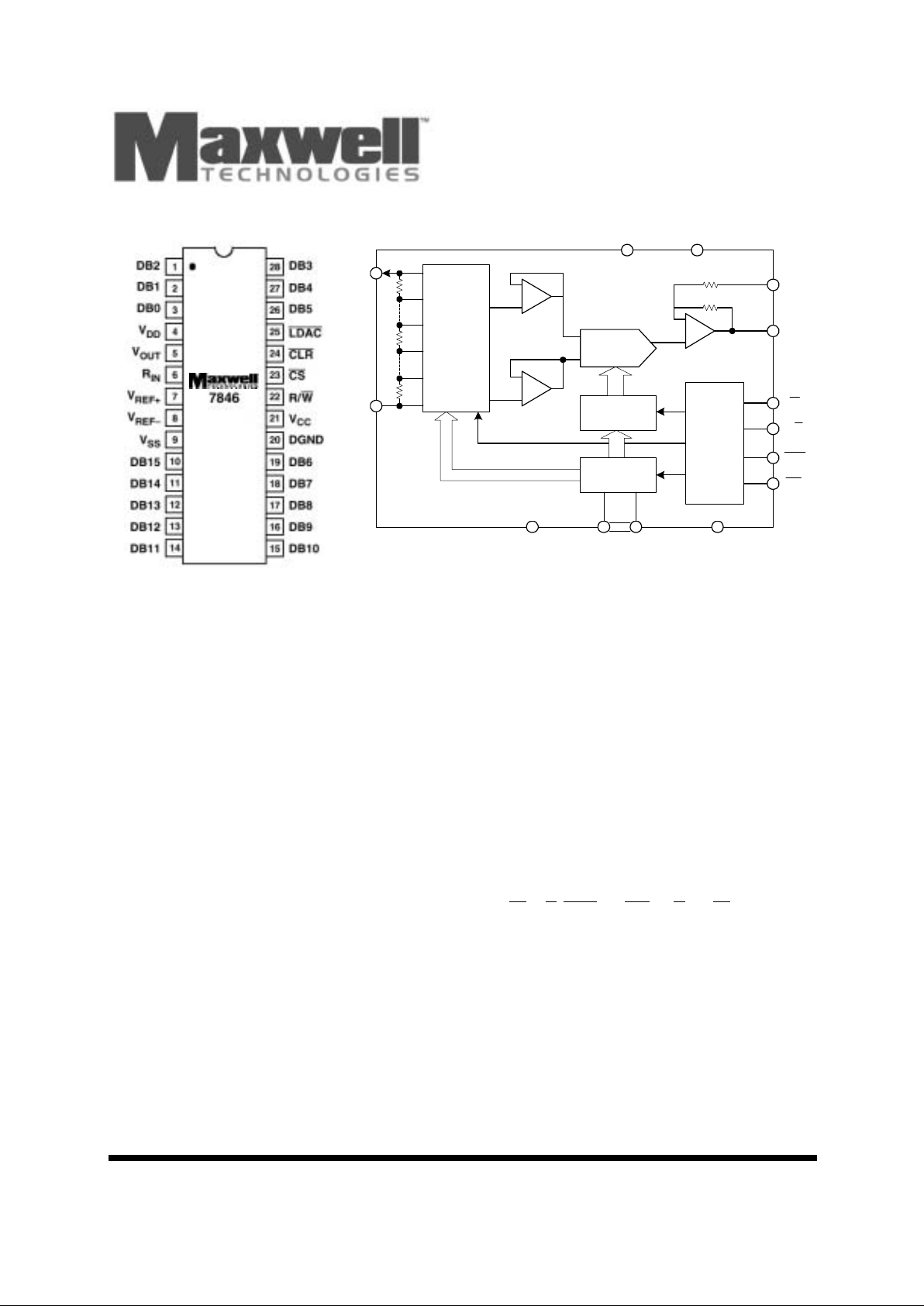
Maxwell T echnologies’ 7846 16-Bit DAC converter microcircuit
features a greater than 100 krad (Si) total dose tolerance,
depending upon space mission. The 7846 has V
REF+
and
V
REF-
reference inputs and an on-chip output amplifier which
gives the option of unipolar or bipolar output. The 7846 uses a
segmented architecture. The 4 MSBs in the DAC latch select
one of the segments in a 16-resistor string. Both taps of the
segment are buffered by amplifiers and fed to a 12-bit DAC,
which provides a further 12 bits of resolution. This architecture
ensures 16-bit monotonicity. Excellent integral linearity results
from tight matching between the input offset voltages of the
two buffer amplifiers. In addition to the excellent accuracy
specifications, the 7846 also offers a comprehensive microprocessor interface. There are 16 data I/O pins, plus control
lines (CS
, R/W, LDAC and CLR). R/W and CS have readback
function which allows writing to and reading from the I/O latch.
Maxwell Technologies' patented R
AD-PAK® packaging technol-
ogy incorporates radiation shielding in the microcircuit package. It eliminates the need for box shielding while providing
the required radiation shielding for a lifetime in orbit or space
mission. In a GEO orbit, R
AD-PAK provides greater than 100
krad (Si) radiation dose tolerance. This product is available
with screening up to Class S.
16
Segment
Switch
Matrix
Control
Logic
A2
A1
A3
I/O Latch
DAC Latch
12-bit DAC
+
+
+
R
R
6
5
23
22
25
24
203109
8
7
21 4
V
DD
V
CC
V
REF+
V
REF-
V
SS
DB15 DB0 DGND
CLR
LDAC
R/W
CS
V
OUT
R
IN
12
12
4
R
R
R
Logic Diagram
Page 2
M
e
m
ory
2All data sheets are subject to change without notice
©2001 Maxwell Technologies
All rights reserved.
16-Bit Digital to Analog Converter
7846
12.19.01 R ev 3
1000602
TABLE 1. 7846 PINOUT DESCRIPTION
PIN SYMBOL DESCRIPTION
1-3 DB2-DB0 Data I/O pins. DB0 is LSB.
4V
DD
Positive supply for analog circuitry. This is +15V nominal.
5V
OUT
DAC output voltage pin.
6R
IN
Input to summing resistor of DAC output amplifier. This is used
to select output voltage ranges.
7V
REF+
V
REF+
Input. The DAC is specified for V
REF+
= +5V.
8V
REF-
V
REF-
Input. For unipolar operation connect V
REF-
to 0V and for
bipolar operation connect it to -5V. The device is specified for
both conditions.
9V
SS
Negative supply for the analog circuitry. This is -15V nominal.
10-19 DB15-DB6 Data I/O pins. DB15 is MSB.
20 DGND Ground pin for digital circuitry.
21 V
CC
Positive supply for digital circuitry . This is +5V nominal.
22 R/W
R/W Input. This can be used to load data to the DAC or to read
back the DAC latch contents.
23 CS
Chip select input. This selects the device.
24 CLR
Clear Input. The DAC can be cleared to 000...000 or
100...000.
25 LDAC
Asynchronous load input to DAC.
26-28 DB5-DB3 Data I/O pins.
Page 3
M
e
m
ory
3All data sheets are subject to change without notice
©2001 Maxwell Technologies
All rights reserved.
16-Bit Digital to Analog Converter
7846
12.19.01 R ev 3
1000602
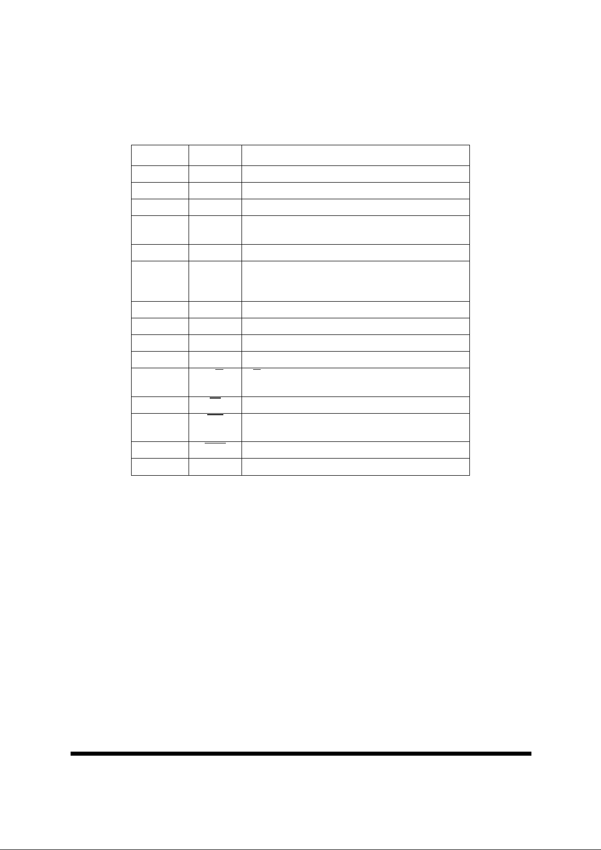
TABLE 2. 7846 A BSOLUTE MAXIMUM RATINGS
1
1. Stresses above those listed under “Absolute Maximum Ratings” may cause permanent damage to the device. This is a stress
rating only and functional operation of the device at these or any other conditions above those i ndicated in the oper ati onal sections of this specification is not implied. Exposure to absolute maximum rating conditions for extended periods of time may
affect device reliability. Only one absolute maximum rating may be applied at any one time.
P
ARAMETER MIN MAX UNIT
VDD to DGND -0.3 +17 V
V
CC
to DGNDp c v c -0.3 VDD +0.3 or 7
(Whichever Is
Lower)
V
V
SS
to DGND -17 +0.3 V
V
REF+
to DGND -25 +2 5 V
V
REF-
to DGND -25 +2 5 V
V
OUT
to DGND
2
2. V
OUT
may be shorted to DGND, VDD, VSS and VCC provided that the power dissipation of the package is not exceeded.
-25 +25 V
R
IN
to DGND -25 +25 V
Digital Input Voltage to DGND -0.3 V
CC
+0.3 V
Digital Output Voltage to DGND -0.3 V
CC
+0.3 V
Power Dissipation (Any Package)
To +75
°
C
Derates above +75
°
C
1000
10
mW
mW/°C
Thermal Inpedance
Θ
JC
2.78 °C
Operating Temperature Range -55 +125
°
C
Storage Temperature Range -65 +150
°
C
TABLE 3. DELTA LIMITS
PARAMETER VARIATION
I
DD
± 10% of value specified in Table 4.
I
EE
± 10% of value specified in Table 4.
I
CC
± 10% of value specified in Table 4.
Page 4

M
e
m
ory
4All data sheets are subject to change without notice
©2001 Maxwell Technologies
All rights reserved.
16-Bit Digital to Analog Converter
7846
12.19.01 R ev 3
1000602
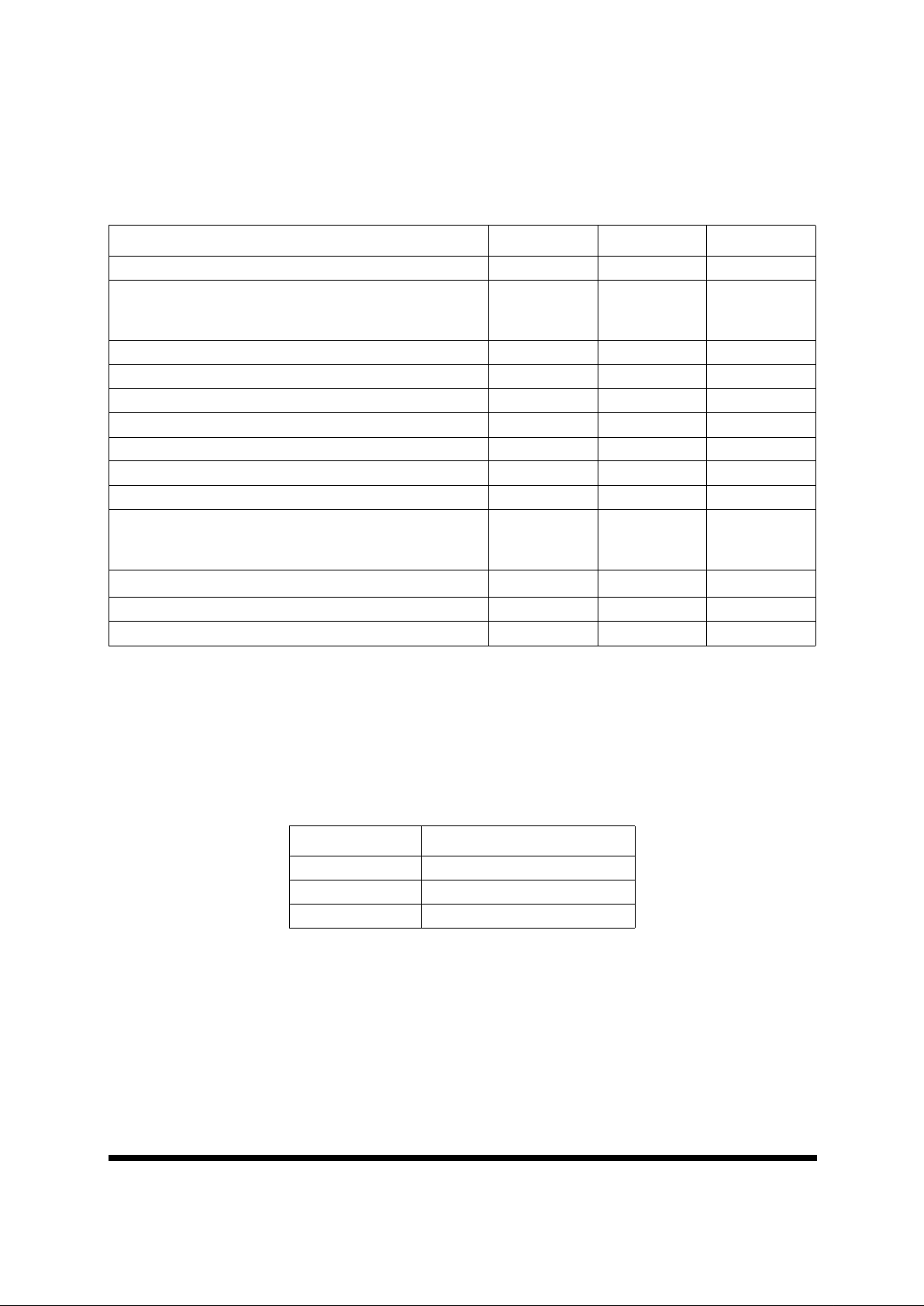
TABLE 4. 7846 ELECTRICAL SPECIFICAT IONS
1
(VCC = +5 V ±5%, TA = -55 TO +125° C )
P
ARAMETER TEST CONDITIONS/COMMENTS
TA=-55 °C TO +125
°
C
U
NIT
Resolution 16 Bits
UNIPOLAR OUTPUT
Relative Accuracy @ 25
°
C
- T
MIN
to T
MAX
Differential Nonlinearity Error
Gain Error @ 25
°
C
- T
MIN
to T
MAX
Offset Error @ 25
°
C
- T
MIN
to T
MAX
Gain TC
2
Offset TC
2
V
REF-
=0V, V
OUT
=0V to +10V
1LSB=153µV
Guaranteed Monotonic
V
OUT
Load= 10MΩ
±16
±16
±1
±12
±24
±12
±24
±2
±2
LSB typ
LSB max
LSB max
LSB typ
LSB max
LSB typ
LSB max
ppm FSR/°C typ
ppm FSR/°C typ
BIPOLAR OUT P UT
Relative Accuracy @ 25
°
C
- T
MIN
to T
MAX
Differential Nonlinearity Error
Gain Error @ 25
°
C
- T
MIN
to T
MAX
Offset Error @ 25
°
C
- T
MIN
to T
MAX
Bipolar Zero Error @ 25 °C
- T
MIN
to T
MAX
Gain TC
2
Offset TC
2
Bipolar Zero TC
2
V
REF-
=-5V, V
OUT
=-10V to +10V
1LSB=305µV
Guaranteed Monotonic
V
OUT
Load=10MΩ
V
OUT
Load=10MΩ
±6
±8
±1
±6
±16
±6
±16
±6
±16
±2
±2
±2
LSB typ
LSB max
LSB max
LSB typ
LSB max
LSB typ
LSB max
LSB typ
LSB max
ppm FSR/
°
C typ
ppm FSR/
°
C typ
ppm FSR/
°
C typ
REFERENCE INPUT
Input Resistance
V
REF+
Range
V
REF-
Range
Resistance from V
REF-
to V
REF+
Typically 30kΩ
20
40
V
SS
+ 6 to VDD - 6
V
SS
+ 6 to VDD - 6
K
Ω min
K
Ω max
V
V
OUTPUT CHARAC T ERISTI CS
Output Voltage Swing
Resistive Load
1
Capacitive Load
3
Output Resistance
Short Circuit Current
To 0V
To 0V
To 0V or Any Power Supply
V
SS
+ 4 to VDD - 3
3
1000
0.3
±25
V max
k
Ω min
pF max
Ω typ
mA typ
DIGITAL INPUTS
V
IH
(Input High Voltage)
V
IL
(Input Low Voltage)
I
IN
(Input Current)
C
IN
(Input Capacitance)
2
2.4
0.8
±10
10
V min
V max
µA max
pF max
DIGITAL OUTPUTS
V
OL
(Output Low Voltage)
V
OH
(Output High Voltage)
Floating State Leakage Current
Floating State Output Capacitance
2
I
SINK
= 1.6mA
I
SOURCE
= 400µA
DB0-DB15 = 0 to V
CC
0.4
4.0
±10
10
V max
V min
µA max
pF max
Page 5

M
e
m
ory
5All data sheets are subject to change without notice
©2001 Maxwell Technologies
All rights reserved.
16-Bit Digital to Analog Converter
7846
12.19.01 R ev 3
1000602
POWER REQUIREMENTS
4
V
DD
V
SS
V
CC
I
DD
I
SS
I
CC
Power Supply Sensitivity
5
Power Dissipation
V
OUT
Unloaded
V
OUT
Unloaded
V
OUT
Unloaded
+11.4/+15.75
-11.4/-15.75
+4.75/+5.25
5
5
1
2
100
V min/V max
V min/V max
V min/V max
mA max
mA max
mA max
LSB/V max
mW typ
1. Minimum load is 3k
Ω.
2. Sample tested to ensure compliance.
3. Maximum load is 1000pF.
4. 7846RP is functional with power supplies of ±12V. See typical performance curves.
5. Sensitivity to Gain Error, Offset Error and Bipolar Zero Error to V
DD
, VSS variations.
6. Guaranteed by design
TABLE 5. 7846 AC PERFORMANCE CHARACTERISTICS
1
(VCC = +5 V ±5%, TA = -55 TO +125° C )
1. Guaranteed by design.
P
ARAMETER TEST CONDITIONS
TA=25°C
T
A=TMIN
TO T
MAX
UNIT
Output Settling Time To 0.006% FSR. V
OUT
loaded. V
REF-
=0V. 7 7 µs max
To 0.003% FSR. V
OUT
loaded. V
REF-
=-5V. 9 9 µs max
Digital-to-Analog Glitch
Impulse
DAC alternately loaded with 10…0000 and
01…1111. V
OUT
unloaded.
400 400 nV-secs typ
AC Feed through V
REF-
=0V, V
REF+
=1V rms, 10kHz sine wave.
DAC loaded with all 0s.
0.5 0.5 mV pk-pk typ
Digital Feed through DAC alternately loaded with all 1s and all
0s. CS High.
10 10 nV-secs typ
Output Noise Voltage Density
(1kHz-100kHz)
Measured at V
OUT
. DAC loaded with
0111011…11.
V
REF+=VREF-
=0V.
50 50 nV/(Hz)
½
typ
TABLE 4. 7846 ELECTRICAL SPECIFICATIONS
1
(VCC = +5 V ±5%, TA = -55 TO +125° C )
P
ARAMETER TEST CONDITIONS/COMMENTS
TA=-55 °C TO +125
°
C
U
NIT
Resolution 16 Bits
Page 6

M
e
m
ory
6All data sheets are subject to change without notice
©2001 Maxwell Technologies
All rights reserved.
16-Bit Digital to Analog Converter
7846
12.19.01 R ev 3
1000602
TABLE 6. 7846 TIMING CHARACT ERISTICS
1,2,3,4
(VDD = +14.25V TO 15.75V; VSS = -14.25V TO -15.75V; VCC = 4.75 TO 5.25V; UNLESS OTHERWISE SPECIFIED)
1. Guaranteed by design. All input control signals are specified with t
R
= tF = 5ns (10% to 90% of +5V) and timed from a voltage
level of 1.6V.
2. t
6
is measured with the load circuits of Figure 1 and defined as the time required for an output to cross 0.8V or 2.4V.
3. t
7
is defined as the time r equir ed for an output to change 0.5V when loaded with the circuits of Figure 2. Specifications subject to
change without notice.
4. See Figure 3 on page 7.
P
ARAMETER TEST CONDITIONS/COMMENTS
LIMIT AT
T
A
=-55 °C TO +125 °C
U
NIT
t
1
R/W to CS Setup Time 50 ns min
t
2
CS Pulse Width (Write Cycle) 190 ns min
t
3
R/W to CS Hold Time 50 ns min
t
4
Data Setup Time 120 ns min
t
5
Data Hold Time 0 ns min
t
6
Data Access Time 320 ns max
t
7
Bus Relinquish Time 10 ns min
90 ns max
t
8
CLR Setup Time 20 ns min
t
9
CLR Pulse Width 150 ns min
t
10
CLR Hold Time 0 ns min
t
11
LDAC Pulse Width 100 ns min
t
12
CS Pulse Width (Read Cycle) 330 ns min
Page 7

M
e
m
ory
7All data sheets are subject to change without notice
©2001 Maxwell Technologies
All rights reserved.
16-Bit Digital to Analog Converter
7846
12.19.01 R ev 3
1000602
FIGURE 1. LOAD CIRCUITS FOR ACCESS TIME (t6)
F
IGURE 2. LOAD CIRCUITS FOR BUS RELINQUISH TIME (t
7
)
FIGURE 3. 16-BIT DIGITAL TO ANALOG CONVERTER
Data Valid
Data Va lid
t
1
t
2
t
t
3
t
12
t
t
t
5
t
6
t
t
t10t
8
t
t
10
t
11
CS
DATA
CLR
LDAC
5V5V0V
Page 8

M
e
m
ory
8All data sheets are subject to change without notice
©2001 Maxwell Technologies
All rights reserved.
16-Bit Digital to Analog Converter
7846
12.19.01 R ev 3
1000602
Page 9

M
e
m
ory
9All data sheets are subject to change without notice
©2001 Maxwell Technologies
All rights reserved.
16-Bit Digital to Analog Converter
7846
12.19.01 R ev 3
1000602
F28-02
Note: All dimensions in inches
28 PIN RAD-PAK® FLAT PACKAGE
SYMBOL
DIMENSION
MIN NOM MAX
A 0.190 0.207 0.224
b 0.015 0.017 0.022
c 0.004 0.005 0.009
D -- 0.720 0.740
E 0.380 0.410 0.420
E1 -- -- 0.440
E2 0.180 0.250 -E3 0.030 0.080 --
e 0.050 BSC
L 0.360 0.370 0.380
Q 0.062 0.073 0.081
S1 0.000 0.027 --
N28
Page 10

M
e
m
ory
10All data sheets are subject to change without notice
©2001 Maxwell Technologies
All rights reserved.
16-Bit Digital to Analog Converter
7846
12.19.01 R ev 3
1000602
Important Notice:
These data sheets are created using the chip manufacturers published specifications. Maxwell Technologies verifies
functional it y by testing key parameters either by 100% testing, sample testing or char acterization.
The specifications presented within these data sheets represent the latest and most accurate information available to
date. However, these specifications are subject to change without notice and Maxwell Technologies assumes no
responsibility for the use of this information.
Maxwell Technologies’ products are not authorized for use as critical components in life support devices or systems
without express written approval from Maxwell Technologies.
Any claim against Maxwell Technologies must be made within 90 days from the date of shipment from Maxwell Technologies. Maxwell Technologies’ liabilit y shall be limited to replacement of defecti ve parts.
Page 11

M
e
m
ory
11All data sheets are subject to change without notice
©2001 Maxwell Technologies
All rights reserved.
16-Bit Digital to Analog Converter
7846
12.19.01 R ev 3
1000602
Product Ordering Options
Model Number
Feature
Option Deta ils
7846
RP
F X
Screening Flow
Package
Radiation Feature
Base Product
Nomenclature
Monolithic
S = Maxwell Class S
B = Maxwell Class B
E = Engineering (testing @ +25°
C)
I = Industrial (testing @ -55°C,
+25°C, +125°C)
F = Flat Pack
RP = R
AD-PAK® package
16-Bit Digital to Analog Converte
r
 Loading...