

Page 1
7820
Microprocessor-compatible
8-Bit ADC
FEATURES:
• 1.36 µs Conversion Time
• Built-in-Track-and-Hold Function
• Single +5 Volt Supply
• No External Clock Required
• Tri-State Output Buffered
• Total Ionization Dose:
- > 50 krads (Si), depending upon space mission.
• Excellent Single Event Effects
- SEL > 80 MeV/mg/cm
• Package:
- 20 pin Rad-Pak DIP
2
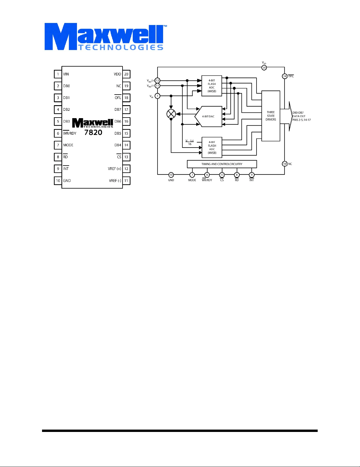
Logic Diagram
DESCRIPTION:
The 7820 is a microprocessor compatible 8-bit Analog-to-Digital Converter with a 0V to +5V input supply range with a single
+5 Volt supply.
The 7820 incorporates internal sample-and-hold circuitry
which eliminates the need for an external S/H for signals with
slew rates less than 100 mV/µs.
The 7820 was designed to be easiliy interfaced with microprocessors, appearing as either a memory location or I/O port
without the need for external interfacing. All outputs are
latched and tri-state buffered.
Maxwell Technologies' patented R
ogy incorporates radiation shielding in the microcircuit package. It eliminates the need for box shielding while providing
the required radiation shielding for a lifetime in orbit or space
mission. In a GEO orbit, R
krad (Si) radiation dose tolerance. This product is available
with screening up to Class S.
AD-PAK® packaging technol-
AD-PAK provides greater than 100
Memory
1000564
(858) 503-3300 - Fax: (858) 503-3301 - www.maxwell.com
12.19.01 Rev2
All data sheets are subject to change without notice
©2001 Maxwell Technologies
All rights reserved.
1
Page 2
Microprocessor-compatible 8-Bit ADC
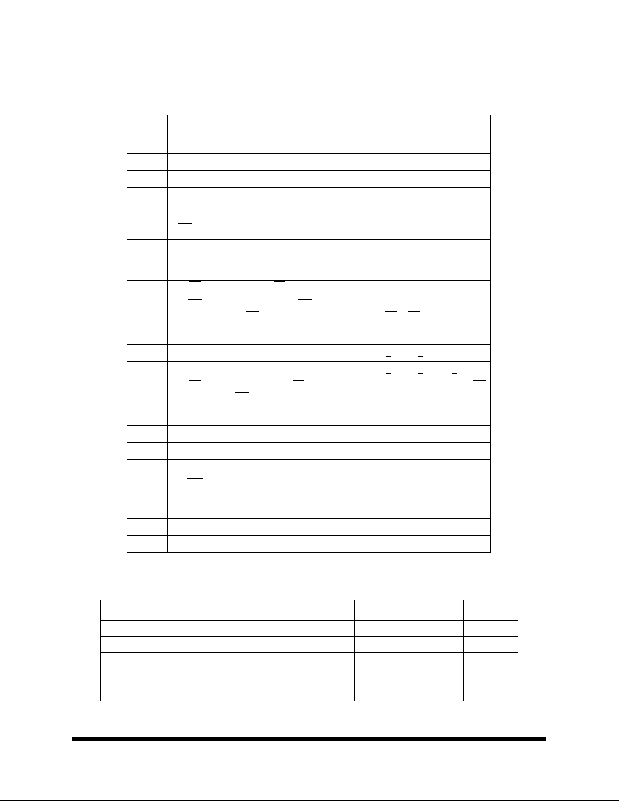
TABLE 1. PIN DESCRIPTION
PIN SYMBOL DESCRIPTION
7820
1VINAnalog Input Range: V
REF(-)
to V
REF(+)
.
2 DB0 Data Output. Three State Output, bit 0 (LSB)
3 DB1 Data Output. Three State Output, bit 1
4 DB2 Data Output. Three State Output, bit 2
5 DB3 Data Output. Three State Output, bit 3
6WR
/RDY WRITE control input/READY status output.
7 Mode Mode Selection Input. It determines whether the device operates in the
WR-RD or RD mode. It is internally tied to GND through a 50 µA current
source.
8RD
9INT
READ Input. RD must be low to access data from the part.
INTERUPT Output. INT going low indicates that the conversion is complete INT
returns high on rising the edge of RD or CS.
10 GND Ground
11 V
12 V
REF-
REF+
Lower limit of reference span. Range: GND < V
Upper limit of reference span. Range: GND < V
REF(-)
REF(-)
< V
< V
REF(+)
REF(+)
< V
DD
13 CS Chip Select Input. CS, the decoded device address, must be low for RD
or WR
to be recognized by the converter.
14 DB4 Data Output. Three State Output, bit 4
15 DB5 Data Output. Three State Output, bit 5
Memory
16 DB6 Data Output. Three State Output, bit 6
17 DB7 Data Output. Three State Output, bit 7 (MSB)
18 OFL
Overflow Output. If the analog input is higher than (V
REF(+)
OFL will be low at the end of conversion. It is a non three state output
which can be used to cascade 2 or more devices to increase resolution.
19 NC No Connection.
20 V
DD
Power supply voltage, +5V
TABLE 2. 7820 ABSOLUTE MAXIMUM RATINGS
1
PARAMETER MIN MAX UNIT
VDD to GND -0 7.0 V
Digital Input Voltage to GND (Pins 6-80, 13) -0.3 V
Digital Output Voltage to GND (Pins 2-5, 9, 14-18) 0.3 V
V
(+) to GND 0 VDD +0.3 V
REF
V
(-) to GND VSS -0.3 V
REF
1000564
12.19.01 Rev2
All data sheets are subject to change without notice
DD
DD
REF
- 1/2LSB),
+0.3 V
+0.3 V
(+) V
2
©2001 Maxwell Technologies
All rights reserved.
Page 3
Microprocessor-compatible 8-Bit ADC
7820
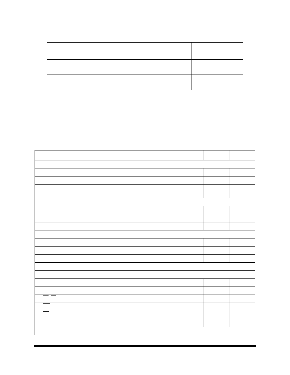
TABLE 2. 7820 ABSOLUTE MAXIMUM RATINGS
1
PARAMETER MIN MAX UNIT
VIN to GND -0.3 VDD +0.3 V
Operating Temperature -55 125 °C
Storage Temperature Range -65 150 °C
Power Dissipation to 75°C -- 450 mW
Derates above +75°C -- 6 mW/°C
1. CAUTION: ESD (electrostatic discharge) sensitive device. The digital control inputs are diode protected; however, permanent damage may occur on unconnected devices subject to high energy electrostatic fields. Unused
devices must be stored in conductive foam or shunts. The protective foam should be discharged to the destination socket before devices are inserted.
TABLE 3. 7820 DC ELECTRICAL CHARACTERISTICS
(VDD = +5V; VREF(+) = +5V; VREF(-) = GND = 0V, UNLESS OTHERWISE SPECIFIED) (RD MODE (PIN 7 = 0V))
(T
= -55 TO 125 °C UNLESS OTHERWISE SPECIFIED)
A
P
ARAMETER TEST CONDITIONS MIN TYP MAX UNIT
Accuracy
Resolution -- 8 -- -- Bits
Total Unadjusted Error
1
-- -- -- ±1.0 LSB
Memory
Minimum Resolution for which No
-- -- -- 8 Bits
Missing Codes are Guaranteed
Reference Input
Input Resisitance -- 1.0 -- 4.0 k
V
(+) Input Voltage Range -- V
REF
V
(-) Input Voltage Range -- GND -- V
REF
(-) -- V
REF
DD
(+) V
REF
Ω
V
Analog Input
Input Voltage Range -- V
(-) -- V
REF
(+) V
REF
Input Leakage Current -- -- -- ±3 µA
Input Capacitance
2
-- -- 45 -- pF
Logic Inputs
CS
, WR, RD
V
INH
V
INH
I
(CS, RD)------1µA
INH
I
(WR)------3µA
INH
I
(WR)-------1µA
INL
Input Capacitance
2
-- 2.4 ----V
-- -- -- 0.8 V
-- -- 5 8 pF
Mode
1000564
12.19.01 Rev2
All data sheets are subject to change without notice
©2001 Maxwell Technologies
All rights reserved.
3
Page 4
Microprocessor-compatible 8-Bit ADC
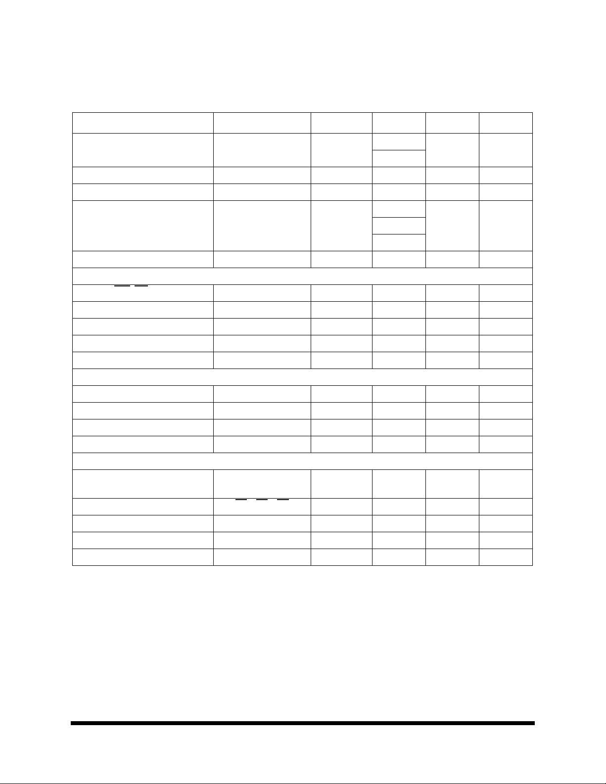
TABLE 3. 7820 DC ELECTRICAL CHARACTERISTICS
(VDD = +5V; VREF(+) = +5V; VREF(-) = GND = 0V, UNLESS OTHERWISE SPECIFIED) (RD MODE (PIN 7 = 0V))
(T
= -55 TO 125 °C UNLESS OTHERWISE SPECIFIED)
A
P
ARAMETER TEST CONDITIONS MIN TYP MAX UNIT
7820
V
INH
-- 3.5 ----V
--
V
INH
I
INH
I
INL
-- -- -- 1.5 V
-- -- -- 200 µA
-- -- -- -1 µA
--
--
Input Capacitance
2
-- -- 5 8 pF
Logic Outputs
DB0-DB7, OFL
V
OH
V
OL
I
(DB0-DB7) Floating State Leakage -- -- ±3 µA
OUT
Output Capacitance
, INT --
ISOURCE = 360 µA 4 -- -- V
ISINK = 1.6 mA -- -- 0.4 V
2
-- -- 5 8 pF
RDY
V
I
OL
OUT
ISINK = 2.6mA -- -- 0.4 V
Floating State Leakage -- -- ±3 V
Output Capacitance -- -- 5 8 pF
Slew Rate, Tracking
2
-- -- 0.2 0.1 V/µs
Power Supply
V
DD
±5% for specified perfor-
-- -- 5 V
mance
Memory
I
DD
CS = RD = OV -- -- 20 mA
Power Dissipation -- -- 40 -- mW
Power Supply Sensitivity VDD = 5V ±5% -- ±1/16 ±1/4 LSB
1. Total unadjusted error includes offset, full scale and linearity error.
2. Not tested.
1000564
12.19.01 Rev2
All data sheets are subject to change without notice
©2001 Maxwell Technologies
All rights reserved.
4
Page 5
Microprocessor-compatible 8-Bit ADC
7820
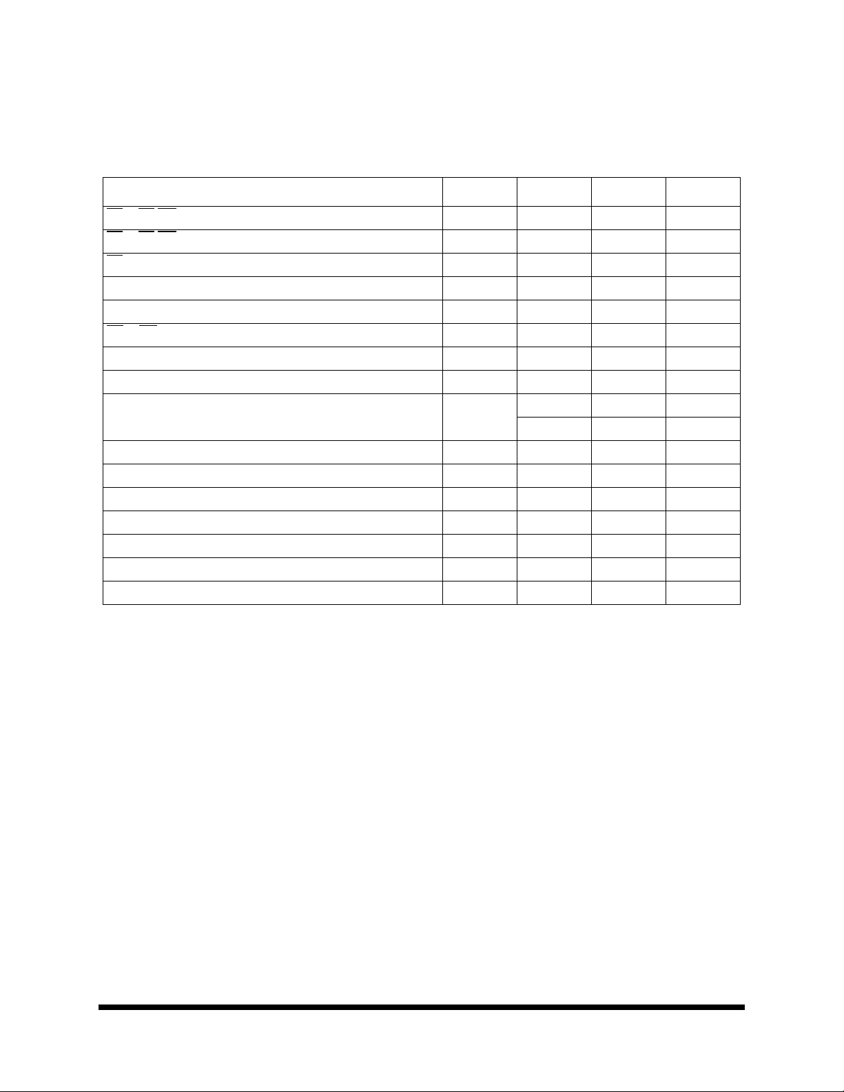
TABLE 4. 7820 AC ELECTRICAL CHARACTERISTICS
1
(VDD = +5V; VREF(+) = +5V; VREF(-) = GND = 0V, UNLESS OTHERWISE SPECIFIED) (RD MODE (PIN 7 = 0V))
(T
= -55 TO 125 °C UNLESS OTHERWISE SPECIFIED)
A
ARAMETER SYMBOL MIN MAX UNIT
P
CS to RD/WR Setup Time t
CS
to RD/WR Hold Time t
CS
to Delay Time (Pull-up Resistor = 5kΩ t
Conversion Time (RD Mode) t
Data Access Time (RD Mode) t
RD
to INT Delay (RD Mode) t
Data Hold Time t
Delay Time Between Conversions t
Write Pulse Width t
CSS
CSH
RDY
CRD
ACCD
INTH
DH
p
WR
0--ns
0--ns
-- 100 ns
-- 2.5 µs
-- t
+ 50 ns
CRD
-- 225 ns
-- 100 ns
600 -- ns
600 -- ns
-- 50 µs
Delay Time Between WR and RD Pulses t
Data Access Time (WR-RD Mode) t
RD to INT Delay t
WR to INT Delay t
Data Access Time (WR-RD Mode) t
WR to INT Delay (Stand-Alone Operation) t
Data Access Time After INT (Stand-Alone Operation t
RD
ACC1
R1
INTL
ACC2
IHWR
ID
700 -- ns
-- 250 ns
-- 225 ns
-- 1700 ns
-- 110 ns
-- 150 ns
-- 75 ns
Memory
1. Sample tested at 25°C to ensure compliance. Only on process design change.
1000564
12.19.01 Rev2
All data sheets are subject to change without notice
5
©2001 Maxwell Technologies
All rights reserved.
Page 6
Microprocessor-compatible 8-Bit ADC
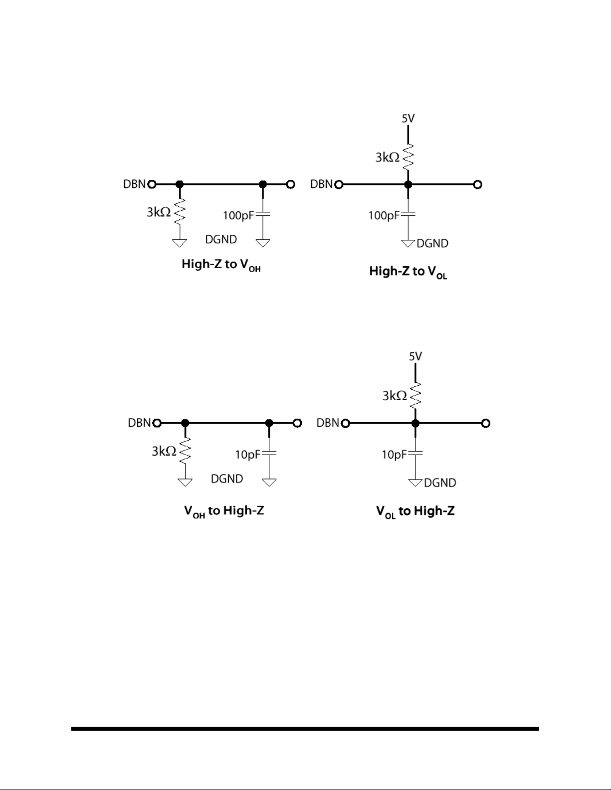
FIGURE 1. LOAD CIRCUITS FOR DATA ACCESS TIME TEST
7820
Memory
FIGURE 2. LOAD CIRCUITS FOR DATA HOLD TIME RESET
1000564
12.19.01 Rev2
All data sheets are subject to change without notice
©2001 Maxwell Technologies
All rights reserved.
6
Page 7
Microprocessor-compatible 8-Bit ADC
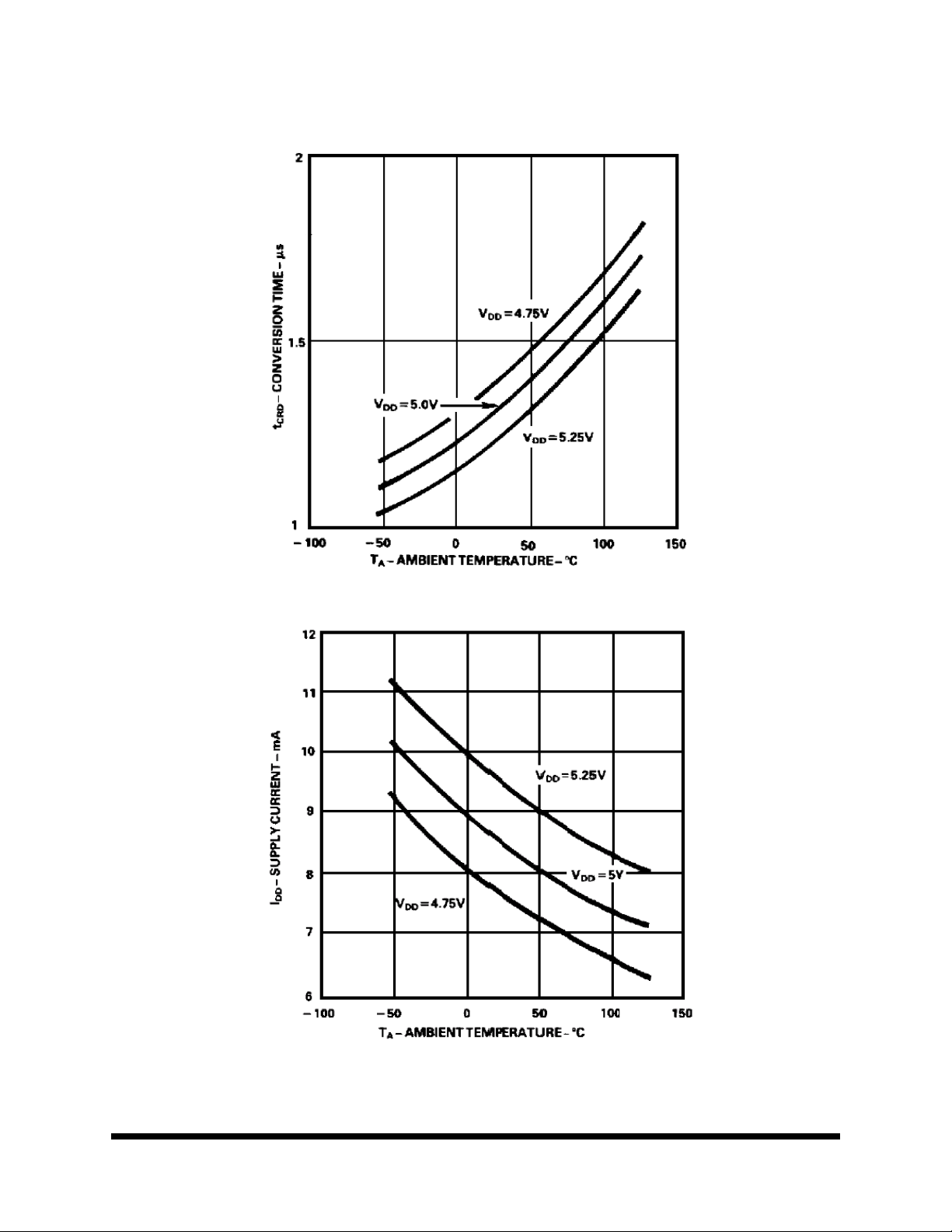
FIGURE 3. LOAD CIRCUIT FOR ACCESS TIME
7820
Memory
FIGURE 4. LOAD CIRCUIT FOR OUTPUT FLOAT DELAY
1000564
12.19.01 Rev2
All data sheets are subject to change without notice
©2001 Maxwell Technologies
All rights reserved.
7
Page 8
Microprocessor-compatible 8-Bit ADC
7820
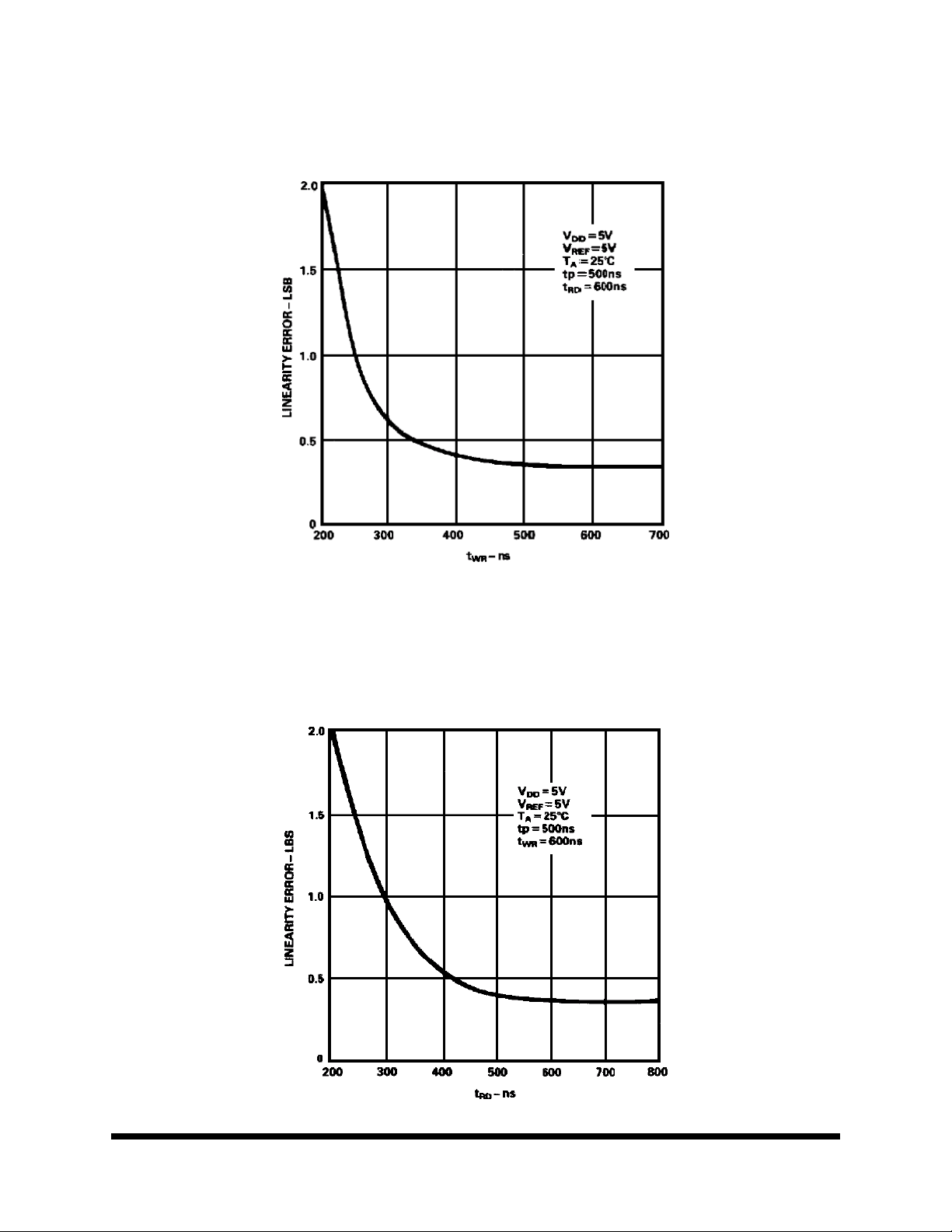
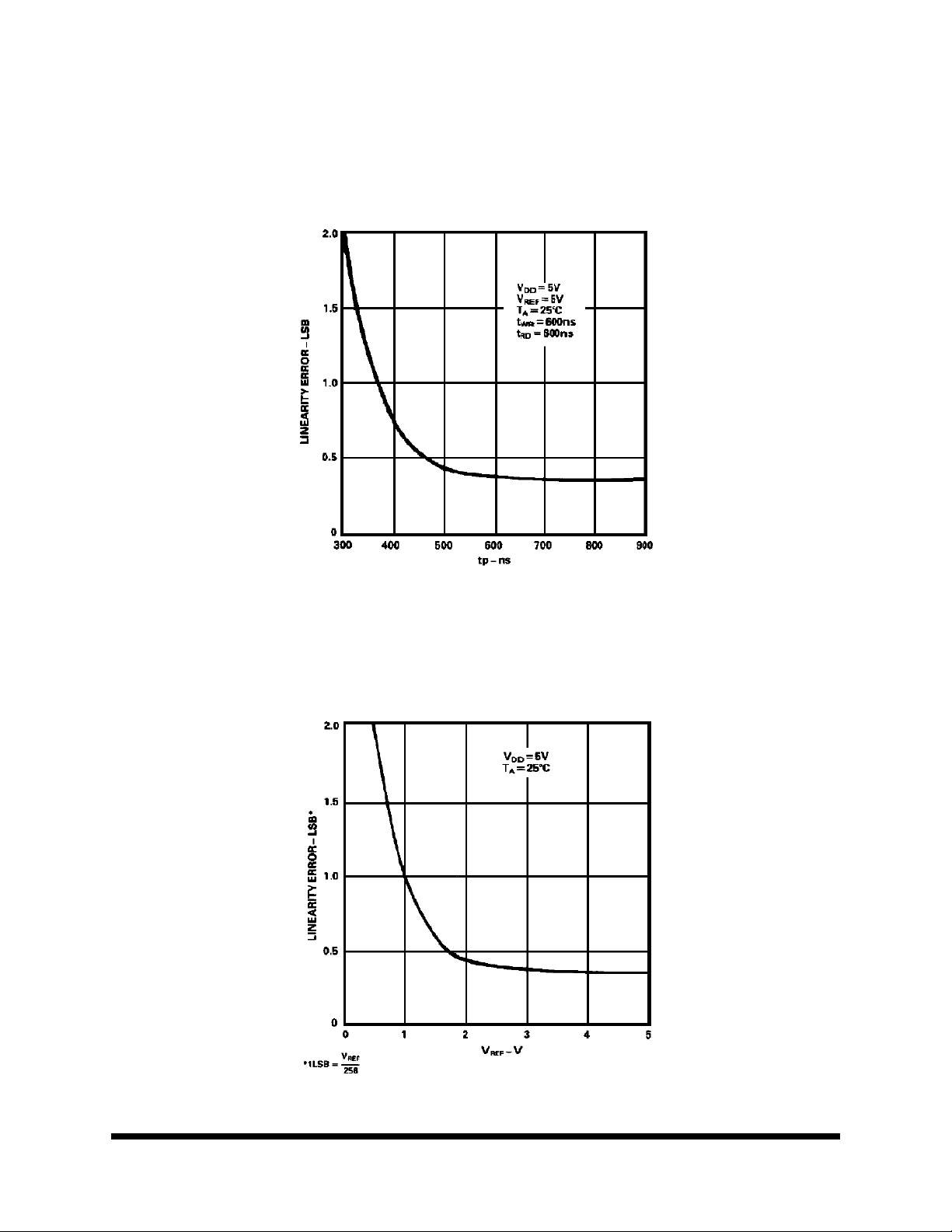
FIGURE 5. ACCURACY VS. T
WR
Memory
1000564
FIGURE 6. ACCURACY VS. T
12.19.01 Rev2
RD
All data sheets are subject to change without notice
8
©2001 Maxwell Technologies
All rights reserved.
Page 9
Microprocessor-compatible 8-Bit ADC
7820
FIGURE 7. ACCURACY VS. T
SP
Memory
FIGURE 8. ACCURACY VS. T
REF [VREF
= V
REF
(+) - V
REF
(-)]
1000564
12.19.01 Rev2
All data sheets are subject to change without notice
©2001 Maxwell Technologies
All rights reserved.
9
Page 10
Microprocessor-compatible 8-Bit ADC
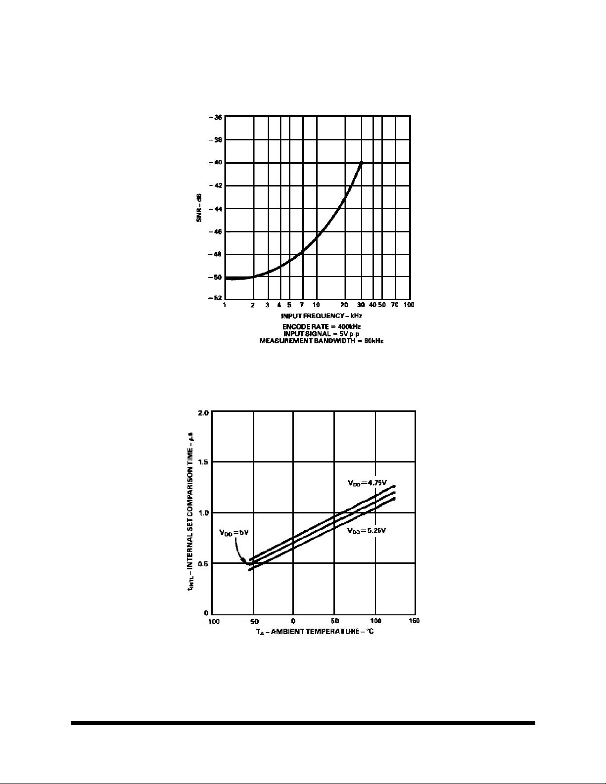
FIGURE 9. SIGNAL-NOISE RATIO VS. INPUT FREQUENCY
7820
Memory
FIGURE 10. T
INTERNAL TIME DELAY VS. TEMPERATURE
INTL
1000564
12.19.01 Rev2
All data sheets are subject to change without notice
©2001 Maxwell Technologies
All rights reserved.
10
Page 11
Microprocessor-compatible 8-Bit ADC
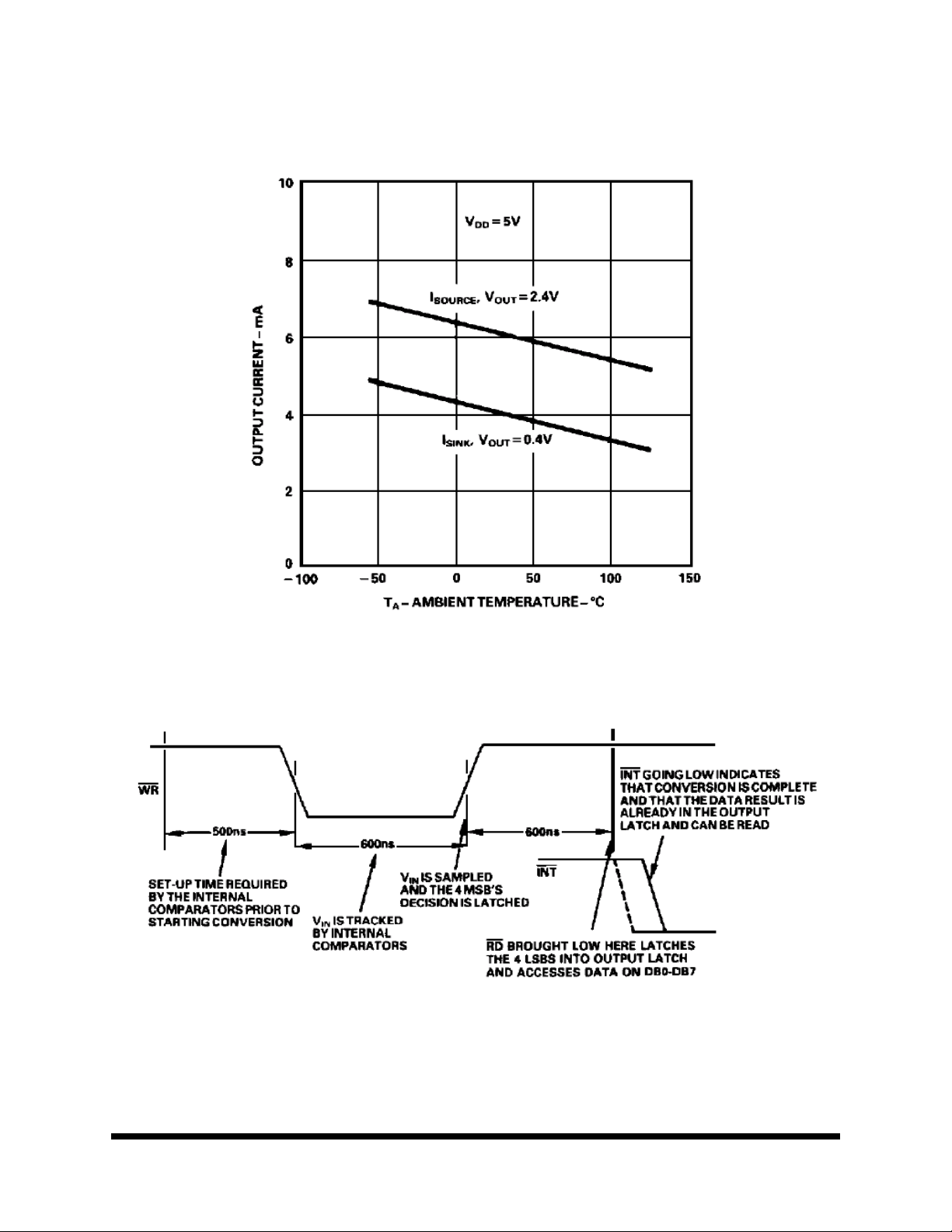
FIGURE 11. OUTPUT CURRENT VS. TEMPERATURE
7820
Memory
FIGURE 12. OPERATING SEQUENCE (WR-RD MODE)
1000564
12.19.01 Rev2
All data sheets are subject to change without notice
©2001 Maxwell Technologies
All rights reserved.
11
Page 12
Microprocessor-compatible 8-Bit ADC
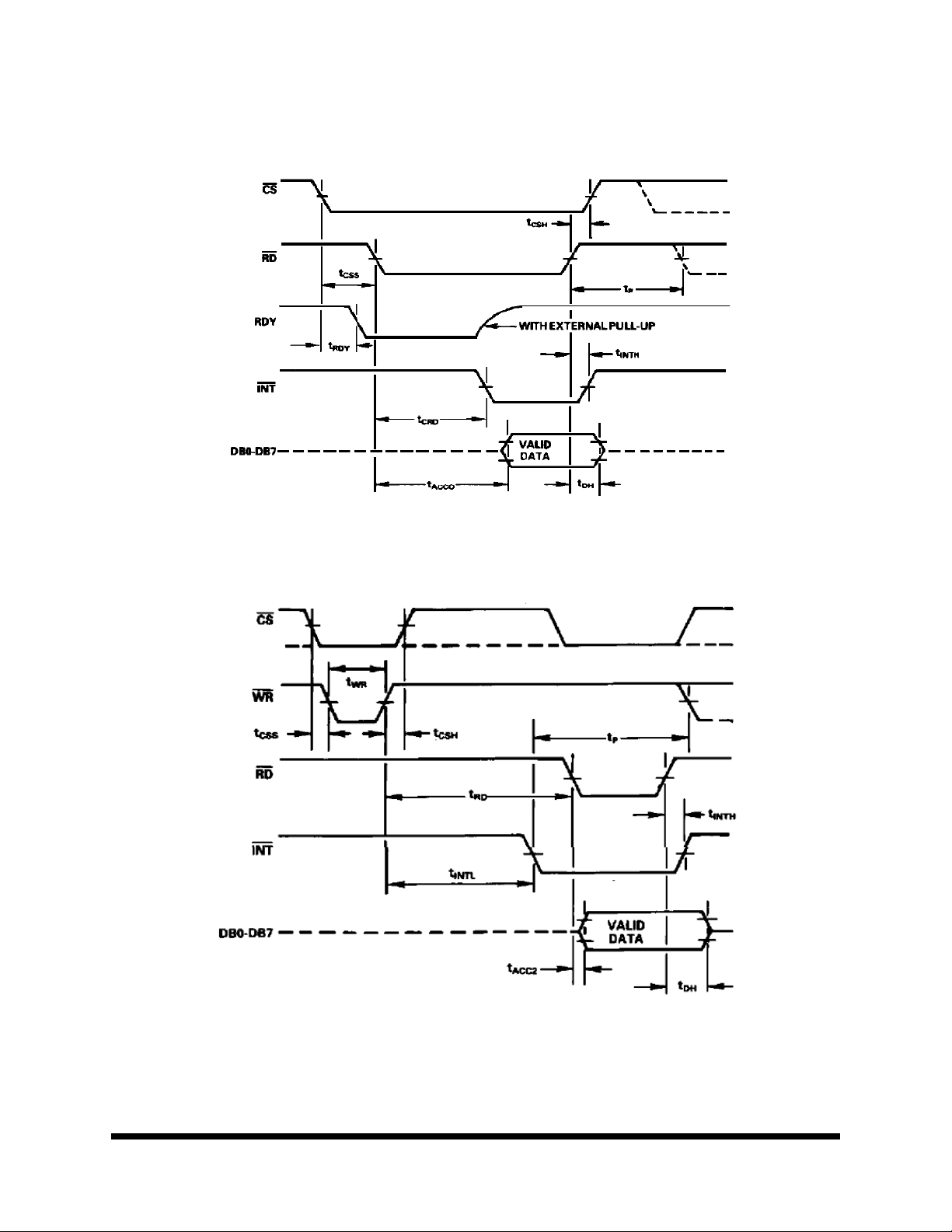
FIGURE 13. RD MODE
7820
Memory
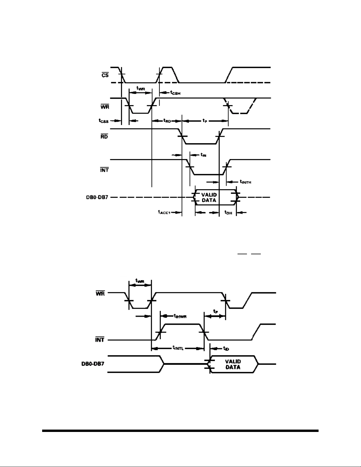
FIGURE 14. WR-RD MODE (TRD>TINTL)
1000564
12.19.01 Rev2
All data sheets are subject to change without notice
©2001 Maxwell Technologies
All rights reserved.
12
Page 13
Microprocessor-compatible 8-Bit ADC
7820
FIGURE 15. WR-RD MODE (TRD<T
INTL
)
Memory
1000564
IGURE 16. WR-RD MODE STAND-ALONE OPERATION (CS=RD=0)
F
12.19.01 Rev2
All data sheets are subject to change without notice
13
©2001 Maxwell Technologies
All rights reserved.
Page 14
Microprocessor-compatible 8-Bit ADC
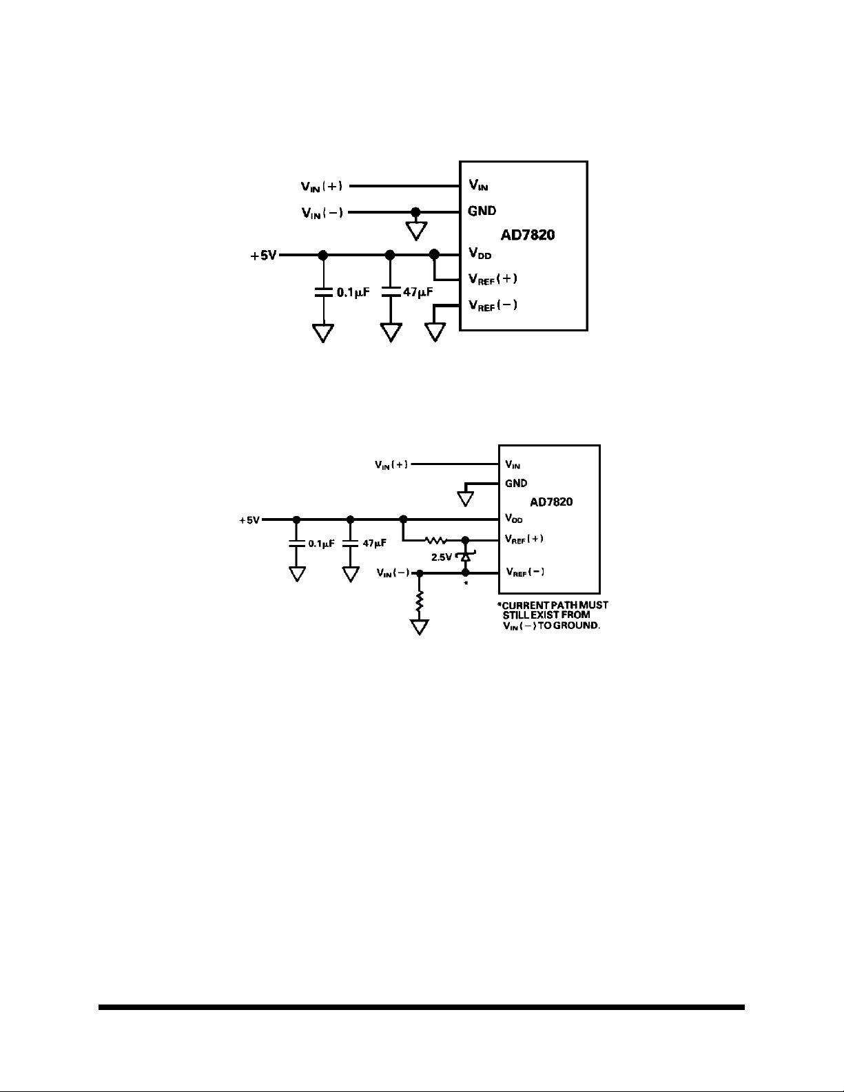
FIGURE 17. POWER SUPPLY AS REFERENCE
FIGURE 18. INPUT NOT REFERENCED TO GND
7820
Memory
1000564
12.19.01 Rev2
All data sheets are subject to change without notice
©2001 Maxwell Technologies
All rights reserved.
14
Page 15
Microprocessor-compatible 8-Bit ADC
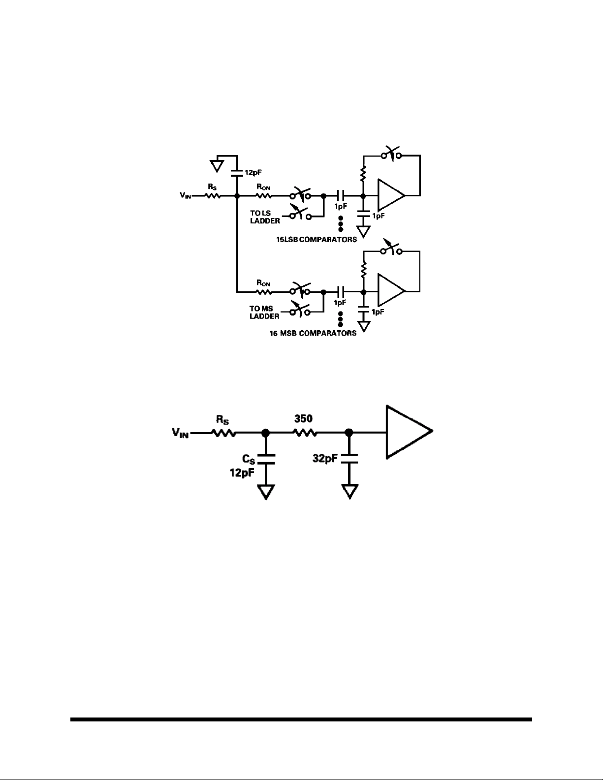
FIGURE 19. EQUIVALENT INPUT CIRCUIT
7820
Memory
FIGURE 20. RC NETWORK MODEL
1000564
12.19.01 Rev2
All data sheets are subject to change without notice
©2001 Maxwell Technologies
All rights reserved.
15
Page 16
Microprocessor-compatible 8-Bit ADC
D
7820
E
N/2
S2
A
Q
S1
e
b2
b
c
L
eA/2
eA
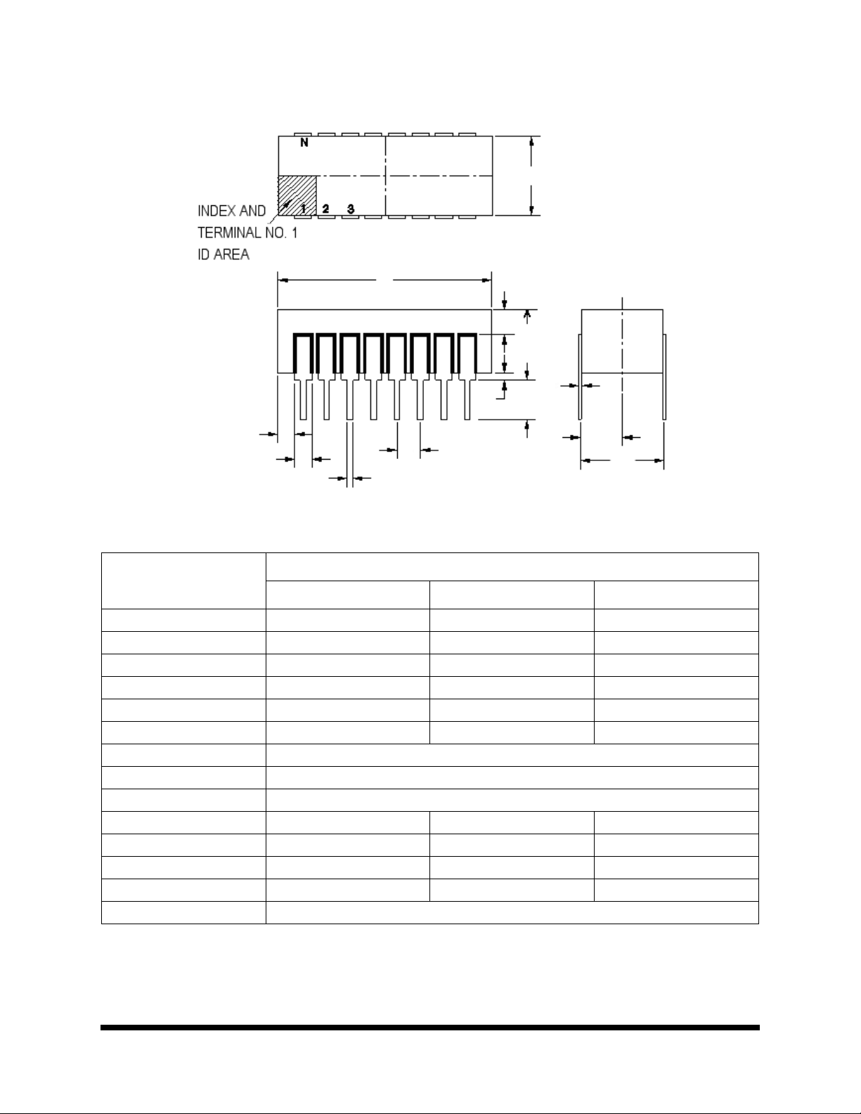
20 PIN RAD-PAK® DUAL IN LINE PACKAGE
SYMBOL
MIN NOM MAX
A -- 0.202 0.230
b 0.014 0.018 0.026
b2 0.045 0.050 0.065
c 0.008 0.010 0.018
D -- 1.000 1.060
E 0.220 0.295 0.310
eA 0.300 BSC
eA/2 0.150 BSC
e 0.100 BSC
L 0.135 0.145 0.155
Q 0.015 0.045 0.070
S1 0.005 0.025 --
S2 0.005 -- --
N20
DIMENSION
Memory
1000564
D16-01
Note: All dimensions in inches
12.19.01 Rev2
All data sheets are subject to change without notice
16
©2001 Maxwell Technologies
All rights reserved.
Page 17

Microprocessor-compatible 8-Bit ADC
Important Notice:
These data sheets are created using the chip manufacturer’s published specifications. Maxwell Technologies verifies
functionality by testing key parameters either by 100% testing, sample testing or characterization.
The specifications presented within these data sheets represent the latest and most accurate information available to
date. However, these specifications are subject to change without notice and Maxwell Technologies assumes no
responsibility for the use of this information.
Maxwell Technologies’ products are not authorized for use as critical components in life support devices or systems
without express written approval from Maxwell Technologies.
Any claim against Maxwell Technologies must be made within 90 days from the date of shipment from Maxwell Technologies. Maxwell Technologies’ liability shall be limited to replacement of defective parts.
7820
Memory
1000564
12.19.01 Rev2
All data sheets are subject to change without notice
©2001 Maxwell Technologies
All rights reserved.
17
Page 18

Microprocessor-compatible 8-Bit ADC
)
Product Ordering Options
Model Number
7820
7820
RP
D X
Feature
Screening Flow
Package
Option Details
Monolithic
S = Maxwell Class S
B = Maxwell Class B
E = Engineering (testing @ +25°C
I = Industrial (testing @ -55°C,
+25°C, +125°C)
Memory
D = Dual In-line Package (DIP)
1000564
Radiation Feature
Base Product
Nomenclature
12.19.01 Rev2
RP = R
AD-PAK® package
Microprocessor-Compatible 8-Bit
ADC
All data sheets are subject to change without notice
18
©2001 Maxwell Technologies
All rights reserved.
 Loading...