

Datasheet 7805ALPRPFS, 7805ALPRPFI, 7805ALPRPFE, 7805ALPRPFB, 7805ALPRPDS Datasheet (MAXWELL)
...Page 1
1
Memory
All data sheets are subject to change without notice
(858) 503-3300 Fax: (858) 503-3301- www.maxwell.com
PRELIMINARY
16-Bit Latchup Protected ADC
7805ALP
©2001 Maxwell Technologies
All rights reserved.
12.19.01 Rev 6
1000583
FEATURES:
• 16-bit organization
• Latchup Protection Technology™
•R
AD-PAK® radiation-hardened against natural space radia-
tion
• Total dose hardness:
- > 50 krads(Si), depending upon space mission
• Latchup converted to reset.
- Rate based on cross section and mission.
• Package:
- 28 pin R
AD-PAK® flat pack
- 28 pin R
AD-PAK® DIP
• 100 kHz min sampling rate
• Standard ± 10V input range
• Advance CMOS technology
- 86 dB min SINAD with 20 kHz input
- Single 5V supply operation
- Utilizes internal or external reference
- Full parallel data output
- Power dissipation: 132 mW max
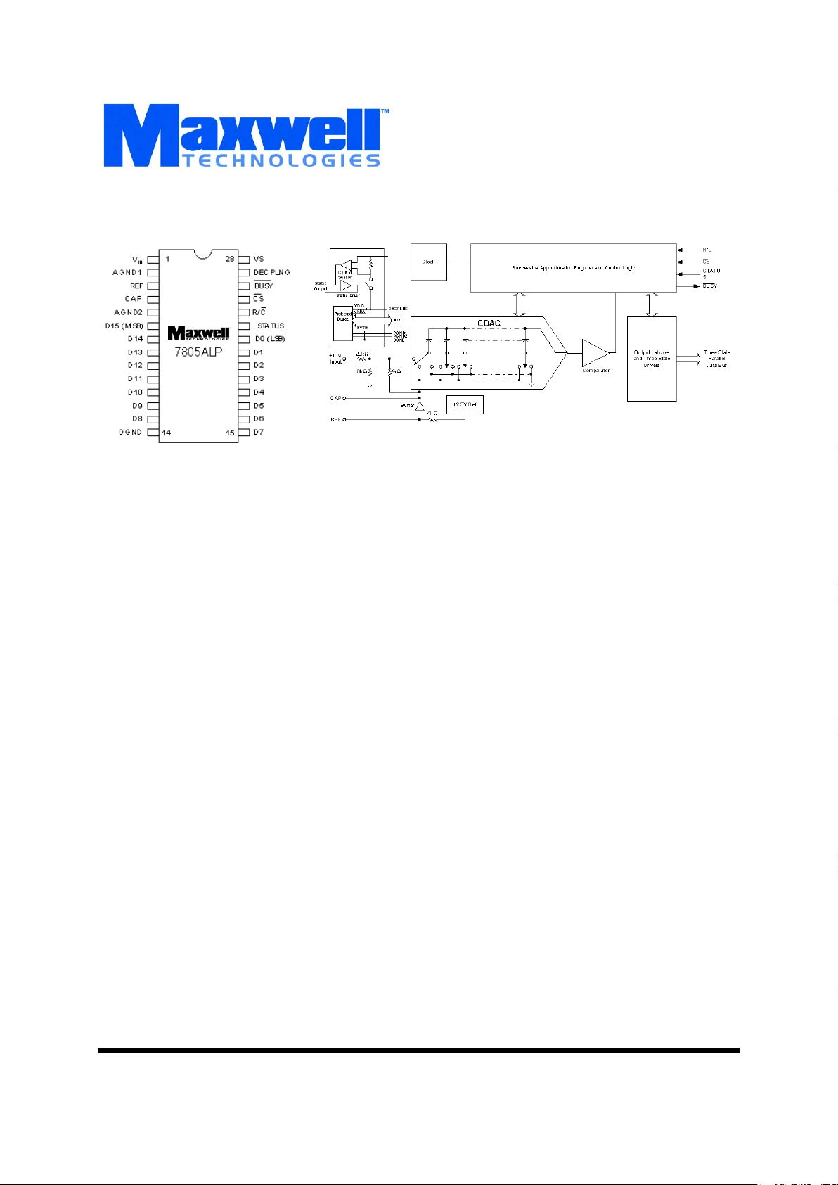
DESCRIPTION:
Maxwell Technologies’ 7805ALP high-speed analog-to-digital
converter features a greater than 50 krad (Si) total dose tolerance, depending upon space mission. Using Mawell’s radiation-hardened R
AD-PAK® packaging technology, the 7805ALP
incorporates the commercial ADS 7805 from Burr Brown. This
device is latchup protected by Maxwell Technologies’ LPT™
technology. The 7805ALP, 16-bit sampling A/D using state-ofthe-art CMOS structure. The device contains a complete 16bit capacitor-based SAR A/D with S/H, reference, clock, interface for microprocessor use, and three-state output drivers.
The 7805ALP is specified at a 100 kHz sampling rate, and
guaranteed over the full temperature range. Laser-trimmed
scaling resistors provide an industry-standard ± 10V input
range, while the innovative design allows operation from a single 5V supply, with power dissipation of under 132 mW.
Maxwell Technologies' patented R
AD-PAK® packaging technol-
ogy incorporates radiation shielding in the microcircuit package. It eliminates the need for box shielding while providing
the required radiation shielding for a lifetime in orbit or space
mission. In a GEO orbit, R
AD-PAK provides greater than 100
krad (Si) radiation dose tolerance. This product is available
with screening up to Class S.
Logic Diagram
Page 2

Memory
PRELIMINARY
2
All data sheets are subject to change without notice
©2001 Maxwell Technologies
All rights reserved.
16-Bit Latchup Protected ADC
7805ALP
12.19.01 Rev 6
1000583
TABLE 1. 7805ALP PINOUT DESCRIPTION
PIN NUMBER NAME DIGITAL I/O DESCRIPTION
1V
IN
Analog input.
2 AGND1 Analog ground. Used internally as ground reference point.
3 REF Reference input/output. 2.2 µF tantalum capacitor to ground
4 CAP Reference buffer capacitor. 2.2 µF tantalum capacitor to ground.
5 AGND2 Analog ground.
6 D15 (MSB) 0 Data bit 15. Most Significant Bit (MSB) of conversion results. When STATUS is
HIGH*, D15 must not be driven high.
7 D14 0 Data bit 14. When STATUS is HIGH*, D14 must not be driven high.
8 D13 0 Data bit 13. When STATUS is HIGH*, D13 must not be driven high.
9 D12 0 Data bit 12. When STATUS is HIGH*, D12 must not be driven high.
10 D11 0 Data bit 11. When STATUS is HIGH*, D11 must not be driven high.
11 D10 0 Data bit 10. When STATUS is HIGH*, D10 must not be driven high.
12 D9 0 Data bit 9. When STATUS is HIGH*, D9 must not be driven high.
13 D8 0 Data bit 8. When STATUS is HIGH*, D8 must not be driven high.
14 DGND Digital Ground
15 D7 0 Data bit 7. When STATUS is HIGH*, D7 must not be driven high.
16 D6 0 Data bit 6. When STATUS is HIGH*, D6 must not be driven high.
17 D5 0 Data bit 5. When STATUS is HIGH*, D5 must not be driven high.
18 D4 0 Data bit 4. When STATUS is HIGH*, D4 must not be driven high.
19 D3 0 Data bit 3. When STATUS is HIGH*, D3 must not be driven high.
20 D2 0 Data bit 2. When STATUS is HIGH*, D2 must not be driven high.
21 D1 0 Data bit 1. When STATUS is HIGH*, D1 must not be driven high.
22 D0 (LSB) 0 Data bit 0. Least Significant Bit (LSB) of conversion results. When STATUS is
HIGH*, D0 must not be driven high.
23 STATUS* 0 STATUS when HIGH indicates latchup protection is active and output data is
invalid. Capacitive loading should not exceed 1000 pF.
24 R/C
IWith CS LOW and BUSY HIGH, a falling edge of R/C initiates a new conversion.
When STATUS is HIGH*, CS
and R/C must not be driven high.
25 CS
I Internally OR’d with R/C. If R/C LOW, a falling edge on CS initiates a new conver-
sion. When STATUS is HIGH*, CS
and R/C must not be driven high.
26 BUSY
0 At the start of a conversion, BUSY goes LOW and stays LOW until the conversion
is completed and the digital outputs have been updated.
27 DECPLNG Supply voltage high speed decoupling pin. Decouple to ground with 1.0 µF ceramic
capacitor.
28 V
S
Supply input. Nominally 5V. Decouple to ground with 10 µF tantalum capacitor.
Page 3
Memory
PRELIMINARY
3
All data sheets are subject to change without notice
©2001 Maxwell Technologies
All rights reserved.
16-Bit Latchup Protected ADC
7805ALP
12.19.01 Rev 6
1000583
TABLE 2. 7805ALP ABSOLUTE MAXIMUM RATINGS
PARAMETER SYMBOL MIN TYP MAX UNIT
Analog Inputs V
IN
CAP
REF
-25
V
S
9
--
--
--
25
AGND2 - 0.3
--
V
Ground Voltage Difference DGND
AGND1
AGND2
-0.3
-0.3
-0.3
--
--
--
0.3
0.3
0.3
V
Supply Input V
S
-- 7 V
Digital Inputs -0.3 -- VS + 0.3 V
Internal Power Dissipation -- -- 825 mW
Maximum Junction Temperature T
J
-- -- 165
°
C
TABLE 3. 7805ALP DC ACCURACY SPECIFICATIONS
PARAMETER CONDITIONS MIN TYP MAX UNIT
Integral Linearity Error -- -- ±3 LSB
Differential Linearity Error -- -- 4, -1 LSB
No Missing Codes
1
1. Not tested.
15 -- -- Bits
Transition Noise
2
2. Typical rms noise at worst case transitions and temperatures.
-- 1.3 -- LSB
Full Scale Error
3,4
3. Measured with various fixed resistors.
4. Full scale error is worst case - Full Scale or +Full Scale untrimmed deviation from ideal first and last code transitions, divided
by the transition voltage (not divided by the full-scale range) and included the effect of offset error.
-- -- ±0.5 %
Full Scale Error Drift -- ±7 -- ppm/
°
C
Bipolar Zero Error
3
-- -- ±10 mV
Bipolar Zero Error Drift -- ±2 -- ppm/
°
C
Power Supply Sensitivity 4.8V < V
S
< 5.25V -- -- ±8 LSB
TABLE 4. 7805ALP DIGITAL INPUTS
PARAMETER MIN TYP MAX UNIT
V
IL
-0.3 -- 0.8 V
V
IH
2.0 -- VS +0.3 V
I
IL
, I
IH
-- -- ±10 µA
Page 4
Memory
PRELIMINARY
4
All data sheets are subject to change without notice
©2001 Maxwell Technologies
All rights reserved.
16-Bit Latchup Protected ADC
7805ALP
12.19.01 Rev 6
1000583
TABLE 5. 7805ALP ANALOG INPUTS
PARAMETER MIN TYP MAX UNIT
Voltage Ranges
1
1. Tested by application of signal.
-10 ±10 10 V
Impedance -- 23 -- k
Ω
Capacitance -- 35 -- pF
TABLE 6. 7805ALP THROUGHPUT SPEED
PARAMETER MIN TYP MAX UNIT
Conversion Time -- 7.6 8 µs
Complete Cycle (Acquire and Convert) -- -- 10 µs
Throughput Rate
1
1. Not tested.
100 -- -- kHz
TABLE 7. 7805ALP AC ACCURACY SPECIFICATIONS
PARAMETER TEST CONDITIONS MIN TYP MAX UNIT
Spurious-Free Dynamic Range
1,2
1. All specifications in dB are referred to a full-scale 10V input.
2. Guaranteed by design.
f
IN
= 45 kHz 90 -- -- dB
Total Harmonic Distortion
1,2
f
IN
= 45 kHz -- -- -90 dB
Signal-to-(Noise + Distortion)
1,2
f
IN
= 45 kHz 83 -- -- dB
-60dB Input -- 30 --
Signal-to-Noise
1,2
f
IN
= 45 kHz 83 -- -- dB
Full-Power Bandwidth
3
3. Full-power bandwidth defined as full-scale input frequency at which signal-to-(noise + distortion) degrades to 60 dB or 10 bits
of accuracy.
-- 250 -- kHz
TABLE 8. 7805ALP SAMPLING DYNAMICS
PARAMETER TEST CONDITIONS MIN TYP MAX UNIT
Aperture Delay -- 40 -- nS
Transient Response FS Step -- 2 -- µS
Overvoltage Recovery
1
1. Recovers to specified performance after 2 x fS input overvoltage.
-- 150 -- nS
Page 5
Memory
PRELIMINARY
5
All data sheets are subject to change without notice
©2001 Maxwell Technologies
All rights reserved.
16-Bit Latchup Protected ADC
7805ALP
12.19.01 Rev 6
1000583
TABLE 9. 7805ALP REFERENCE
PARAMETER MIN TYP MAX UNIT
Internal Reference Voltage 2.48 2.5 2.52 V
Internal Reference Source Current (Must use external buffer) -- 1 -- µA
Internal Reference Drift -- 8 -- ppm/
°
C
External Reference Voltage Range for Specified Linearity
1
1. Tested by application of signal.
-- 2.5 -- V
External Reference Current Drain
2
2. Not tested.
-- -- 100 µA
TABLE 10. 7805ALP DIGITAL OUTPUTS
PARAMETER TEST CONDITIONS MIN TYP MAX UNIT
Data Formatting (Parallel 16-bits Binary Two’s Complement)
Data Coding Binary Two’s Complement
V
OL
(I
SINK
= 1.6mA) 4.0 -- -- 0.4 V
V
OH
(I
SOURCE
= -400 µA) 4.0 -- -- V
Leakage Current High-Z State, V
OUT
= 0V
to V
S
-- -- ±5 µA
Output Capacitance High-Z State -- 10 -- pF
TABLE 11. 7805ALP POWER SUPPLIES
PARAMETER TEST CONDITIONS MIN TYP MAX UNIT
V
S
4.8 5 5.25 V
I
S
-- 20.3 -- mA
Power Dissipation f
S
= 100 kHz -- 102 132.0 mW
TABLE 12. 7805ALP DIGITAL TIMING
PARAMETER MIN TYP MAX UNIT
Bus Access Time -- -- 83 nS
Bus Relinquish Time -- -- 83 nS
Page 6
Memory
PRELIMINARY
6
All data sheets are subject to change without notice
©2001 Maxwell Technologies
All rights reserved.
16-Bit Latchup Protected ADC
7805ALP
12.19.01 Rev 6
1000583
TABLE 13. 7805ALP TEMPERATURE
PARAMETER MIN TYP MAX UNIT
Specified Performance -40 -- 85
°
C
Derated Performance
1
1. Tested by application of signal.
-55 -- 125
°
C
Storage -65 -- 150
°
C
TABLE 14. 7805ALP CONVERSION TIMING
1
1. Tested by application of signal.
D
ESCRIPTION SYMBOL MIN TYP MAX UNIT
Convert pulse width t
1
40 -- 7000 ns
Data valid delay after R/C
low t
2
-- -- 8 µs
BUSY
delay from R/C low t
3
-- -- 85 ns
BUSY
low t
4
-- -- 8 µs
BUSY
delay after end-of-conversion t
5
-- 220 -- ns
Aperture time t
6
-- 40 -- ns
Conversion time t
7
-- 7.6 8 µs
Acquisition time t
8
-- -- 2 µs
Bus relinquish time t
9
10 35 83 ns
BUSY
delay after data valid t
10
50 200 -- ns
Previous data valid delay after R/C
low t
11
-- 7.4 -- µs
Throughput time t
7
+ t
8
-- 9 10 µs
R/C
to CS setup time t
12
10 -- -- ns
Time between conversions t
13
10 -- -- µs
Bus access time t
14
10 -- 83 ns
TABLE 15. 7805ALP CONTROL LINE FUNCTION FOR READ AND CONVERT
CS R/C BUSY OPERATION
1 X X None. Databus is in Hi-Z state.
↓ 0 1 Initiates conversion "n". Databus remains in Hi-Z state.
0
↓ 1 Initiates conversion "n". Databus enters Hi-Z state.
01
↓ Conversion "n" completed. Valid data from conversion "n" on the databus.
↓ 1 1 Enables databus with valid data from conversion "n".
↓ 1 0 Enables databus with valid data from conversion "n-1". Conversion "n" in progress.
Page 7

Memory
PRELIMINARY
7
All data sheets are subject to change without notice
©2001 Maxwell Technologies
All rights reserved.
16-Bit Latchup Protected ADC
7805ALP
12.19.01 Rev 6
1000583
FIGURE 1. CONVERSION TIMING WITH OUTPUTS ENABLED AFTER CONVERSION (CS TIED LOW)
0 ↓ 0 Enables databus with valid data from conversion "n-1". Conversion "n" in
progress."
00
↓ New conversion initiated without acquisition of a new signal. Data will be invalid.
CS
and/or R/C must be HIGH when BUSY goes HIGH.
X X 0 New convert commands ignored. Conversion "n" in progress.
TABLE 15. 7805ALP CONTROL LINE FUNCTION FOR READ AND CONVERT
CS R/C BUSY OPERATION
Page 8
Memory
PRELIMINARY
8
All data sheets are subject to change without notice
©2001 Maxwell Technologies
All rights reserved.
16-Bit Latchup Protected ADC
7805ALP
12.19.01 Rev 6
1000583
FIGURE 2. USING CS TO CONTROL CONVERSION AND READ TIMING
LPT™ Operation
Latchup Protection Technology (LPT
™) automatically detects an increase in the supply current of the 7805ALP con-
verter due to a single event effect and internally cycles the power to the converter off, then on, which restores the
steady state operation of the device. A simplified block diagram of the 7805ALP circuitry is shown in Figure 1. The circuitry consists of a protected device, the ADS7805 die, a current sensor, a power switch, and a status output driver.
FIGURE 3. LATCHUP PROTECTION DIAGRAM
VS
I/Os
POWER
SWITCH
PROTECTED
DEVICE
STATUS
OUTPUT
DECPLNGVDIG
VANA
BYTE
ADS7805
7805ALPRP
DGND
AGND2
AGND1
CURRENT
SENSOR
STATUS
DRIVER
Page 9

Memory
PRELIMINARY
9
All data sheets are subject to change without notice
©2001 Maxwell Technologies
All rights reserved.
16-Bit Latchup Protected ADC
7805ALP
12.19.01 Rev 6
1000583
Differences Between the7805A and the ADS7805
Because the 7805A uses the ADS7805 die to perform the analog to digital conversion function its operation and performance is very similar to the ADS7805 packaged part from Burr-Brown. In general the operation and application will
be the same for both parts. There are two primary differences: the operation of the supply pins and the operation of the
BYTE and STATUS pins.
The ADS7805 provides separate analog and digital supply pins. The 7805A provides a single supply input V
S
pin in
place of the V
DIG
pin which powers both the analog and digital circuitry through the LPT™ current sensor and power
switch. The V
S
power supply should be treated as an analog supply and isolated from noise on the system digital
power supply. The low side of the power switch connects to the ADS7805 die power pads and to the package DECPLNG pin which replaces the VANA pin. The DECPLNG pin allows low ESR ceramic capacitors to directly decouple
the ADS7805 die. CAUTION: The DECPLNG pin must not be connected to the power supply since this will defeat the
LPT
™ power switch and could result in latchup of the device during operation in a radiation environment. Electrolytic
capacitors should not be connected to the DECPLNG pin because the large capacitance will increase the recovery
time of the 7805A.
The primary functional difference between the ADS7805 and the 7805A is that the BYTE signal of the ADS7805 is
internally grounded and the pin function is replaced by the STATUS output. Grounding the BYTE signal permanently
assigns the data output signal bits 15:0 as shown in the 7805A pinout diagram where bit15 is the MSB and bit 0 is the
LSB.
A high level STATUS signal indicates that a single event induced latchup current was detected by the LPT
™ circuitry
causing power to be removed from the protected device. CAUTION: During the time that power is removed from the
protected device, it is critical that external circuitry driving the device I/O pins does not backdrive the device supply.
Backdriving the supply could contribute to an extended or even a permanent latchup condition.
In order to prevent backdriving the supply, the STATUS signal should be used in the system to tri-state or gate external
I/O drive circuits to a low state. Similarly, if the data outputs are connected to a bus with other bus driver circuits, all
external data bus drivers must be tri-stated and individual pull up resistors to the supply voltage (if used on the data
bus) must not be less than 10 K
Ω typical to assure proper single event effect recovery. Tri-stating of inputs should
occur within 100 nsec after the rise of the status pin. The BYTE signal can be made available in place of the STATUS
signal at customer request.
STATUS can also be used to generate an input to the system data processor indicating that an LPT
™ cycle has
occurred, and the protected device output accuracy may not be met until after the respective recovery time to the
event. The STATUS signal is generated from an advanced CMOS logic gate output. This output may not exhibit a
monotonic falltime and may even oscillate briefly while power is being restored to the protected device and the decoupling capacitance is charged. Loading on the STATUS output should be minimized because this signal is used internally by the 7805A. It is recommended that load current not exceed 2 mA and load capacitance be kept well below
1000 pF.
A summary of the pin differences between the ADS7805 and 7805A is provided below.
TABLE 16. PIN DIFFERENCES
PIN NUMBER ADS7805 7805A PIN DIFFERENCE DESCRIPTION
23 BYTE STATUS A high level STATUS signal indicates that power is removed from the ADS7805 die.
I/O pins must not be driven high while this signal is active. The BYTE signal of the
ADS7805 die is internally grounded but can also be made available in place of the
STATUS pin at customer request.
Page 10
Memory
PRELIMINARY
10
All data sheets are subject to change without notice
©2001 Maxwell Technologies
All rights reserved.
16-Bit Latchup Protected ADC
7805ALP
12.19.01 Rev 6
1000583
Example Circuits for Using the 7805A
Figure 2 shows a typical application circuit for using the 7805A as an input to a digital data processor. This circuit
shows the use of the STATUS pin to tri-state the control inputs when the latchup protection circuit cycles the power to
the protected ADS7805 die.
Figure 3 shows a typical application circuit for connecting the 7805A to a 16-bit data bus with multiple drivers on the
bus. Tri-state buffers are used to isolate the 7805A data outputs from the data bus. Figure 4 shows the typical application circuit for connecting the 7805A to an 8-bit data bus.
FIGURE 4. TYPICAL 7805A APPLICATION CIRCUIT
27 VANA DECPLNG The ADS7805 VANA and V
DIG
die pads are connected together and are available
at the DECPLNG pin. This pin allows external ceramic capacitors to directly decouple the power inputs to the ADS7805 die-to-analog ground. Decoupling capacitance should not exceed 0.2 uF typical. This pin must not be connected to a power
supply directly since this will defeat the latchup protection circuitry. Electrolytic filter
capacitors should not be connected to this pin but should be connected between
the V
S
pin and ground.
28 V
DIG
V
S
This is the power supply input for the LPT circuitry and the protected ADS7805 die.
This supply should be treated as an analog supply with filtering and/or isolation
from the noisy system digital power supply. The LPT latchup current sense and
power switch circuitry is located between this pin and the DECPLNG pin.
TABLE 16. PIN DIFFERENCES
PIN NUMBER ADS7805 7805A PIN DIFFERENCE DESCRIPTION
Page 11

Memory
PRELIMINARY
11
All data sheets are subject to change without notice
©2001 Maxwell Technologies
All rights reserved.
16-Bit Latchup Protected ADC
7805ALP
12.19.01 Rev 6
1000583
FIGURE 5. TYPICAL 7805A CIRCUIT WITH 16-BIT BUS INTERFACE
FIGURE 6. TYPICAL 7805A CIRCUIT WITH 8-BIT BUS INTERFACE
Testing the 7805A Latchup Protection Circuitry
The DECPLNG pin provides direct access to the 7805ALP converter supply pins for attaching external decoupling
capacitor(s) to ground. This pin can also be used to test the LPT
™ operation by sinking a pulsed current load to
ground as shown in the test circuit in Figure 5 and as described in the LPT Operating Characteristics Table (Table 17)
Page 12

Memory
PRELIMINARY
12
All data sheets are subject to change without notice
©2001 Maxwell Technologies
All rights reserved.
16-Bit Latchup Protected ADC
7805ALP
12.19.01 Rev 6
1000583
and LPT Timing diagram (Figure 7). This test approximates the operation of the 7805A in response to a single event
latchup and recovery.
During the time that the power is cycled, output signals and data from the 7805A are invalid. The STATUS signal HIGH
indicates that power is removed from the ADS7805 die. All input pins must be driven low or tri-stated. When this signal
is low, power is applied to the ADS7805 die. The STATUS signal can be used to measure the supply recovery time.
The status signal can exhibit multiple transitions when power is re-applied and the decoupling capacitors are charged.
The duration and number of transitions is dependent on the amount of capacitance used. The supply recovery time
interval starts when the supply current rises (causing STATUS to go high) and ends when the STATUS signal stabilizes low again.
Within the functional recovery time interval (typically 25 µsec after the LPT circuit reapplies power), the normal functional operation of the converter is restored with less than 5% full scale error. Additional settling time is then required to
return to full accurate operation. Defined recovery time intervals indicate that time to recover first is within 8-bit accuracy, then within 12 bit accuracy, and finally full 16-bit accuracy. These recovery times are primarily due to the single
event and power cycling effects on the reference circuits and the settling times of their respective filter capacitors.
FIGURE 7. LPT™ TEST CIRCUIT
TABLE 17. LPT™ OPERATING CHARACTERISTICS
PARAMETER MIN TYP MAX UNITS
Supply threshold current - ITHR 56 77 99 mA
Protection time (IS Peak = .2A) - TPT -- 1 -- µsec
Input tri-state time - TIOFF -- -- 100 nsec
Status instability time - TINST -- -- 10 µsec
Supply recovery time (IS Peak = .2A) - TSR 25 50 100 µsec
Functional recovery time (IS Peak = .2A) - TFR -- TSR + 25 -- µsec
8-Bit accuracy recovery time (IS Peak = .2A) - T8R -- 75 -- msec
12-Bit accuracy recovery time (IS Peak = .2A) - T12R -- 250 -- msec
Full accuracy recovery time (IS Peak - .2A) - TFAR -- 425 -- msec
Page 13

Memory
PRELIMINARY
13
All data sheets are subject to change without notice
©2001 Maxwell Technologies
All rights reserved.
16-Bit Latchup Protected ADC
7805ALP
12.19.01 Rev 6
1000583
FIGURE 8.
FIGURE 9. SEU AND SEL CROSS SECTION
Page 14

Memory
PRELIMINARY
14
All data sheets are subject to change without notice
©2001 Maxwell Technologies
All rights reserved.
16-Bit Latchup Protected ADC
7805ALP
12.19.01 Rev 6
1000583
AD7805/AD7809 INTERFACE SECTION
The 7805 is a parallel data input device and contains both control registers and data registers. The system control register has global control over all DACs in the package while the channel control register allows control over individual
DACs in the package. Two data registers are also available, one for the 10-bit Main DAC and the second for the 8-bit
Sub DAC. In the parallel mode, CS and WR, in association with the address pins, control the loading of data. Data is
transferred from the data register to the DAC register under the control of the LDAC signal. Only data contained in the
DAC register determines the analog output of any DAC. The timing diagram for 10-bit parallel loading is shown in Figure 2. The MODE pin on the device determines whether writing is to the data registers or to the control registers.
When MODE is at a logic one, writing is to the data registers. In the next write to the data registers a bit in the channel
control register determines whether the Main DAC or the Sub DAC is addressed. This means that to address either
the Main or the Sub DAC the Main/Sub bit in the control register has to be set appropriately before the data register
write. A logic zero on the mode pin enables writing to the control register. Bit MD0 determines whether writing is to the
system control register or to the addressed channel control register.
Bringing the CLR line low resets the DAC registers to one of two known conditions depending on the coding scheme
selected. The hardware clear affects both the Main and Sub DAC registers. With offset binary coding a clear sets the
output of the Main DAC to the bottom of the transfer function, VBIAS/16. With twos complement coding the output of
the DAC is cleared to midscale which is VBIAS. A hardware clear always clears the output of the Sub DAC to midscale
thus the output of the Sub DAC makes zero contribution to the output of the channel.
FIGURE 10. 7805ALP INTERNAL REGISTERS
Page 15

Memory
PRELIMINARY
15
All data sheets are subject to change without notice
©2001 Maxwell Technologies
All rights reserved.
16-Bit Latchup Protected ADC
7805ALP
12.19.01 Rev 6
1000583
7805ALP CONTROL REGISTERS
Access to the control registers of the 7805ALP is achieved by taking the mode pin to a logic low. The control register
of these DACs are configured as in Figures 11 and 12. There are two control registers associated with the part. System control register which looks after the input coding, data format, power down, system clear and system standby.
The channel control register contains bits that affect the operation of the selected DAC. The external address bits are
used to select the DACs. These registers are eight bits wide and the last two bits are control bits. The mode pin must
be low to have access to the control registers.
FIGURE 11. 7805ALP SYSTEM CONTROL REGISTER CONFIGURATION
FIGURE 12. 7805ALP CHANNEL CONTROL REGISTER CONFIGURATION
The external mode pin must be taken high to allow data to be written to the DAC data registers. Figure 13 shows the
bit allocations when 10-bit parallel operation is selected in the system control register.
FIGURE 13. 7805ALP MAIN DAC DATA REGISTER (TOP) AND SUB DAC DATA REGISTER (BOTTOM) CONFIGURATION
(MODE = 1, 10 /8 = 0)
Figure 14 shows the bit allocations when 8-bit parallel operation is selected in the system control register. DB9 to DB2
are retained as data bits. DB1 acts as a high byte or low byte enable. When DB1 is low, the eight MSBs of the data
word are loaded to the input register. When DB1 is high, the low byte consisting of the two LSBs are loaded to the
input register. DB0 is used to select either the Main or Sub DAC when in the byte mode.
Page 16

Memory
PRELIMINARY
16
All data sheets are subject to change without notice
©2001 Maxwell Technologies
All rights reserved.
16-Bit Latchup Protected ADC
7805ALP
12.19.01 Rev 6
1000583
FIGURE 14. 7805ALP MAIN DAC DATA REGISTER CONFIGURATION (MODE = 1, 10 /8 = 1, MAIN/SUB = 0))
Figure 15 shows the bit allocations for writing to the Sub DAC.
FIGURE 15. 7805ALP SUB DAC DATA REGISTER CONFIGURATION (MODE = 1, MAIN /SUB = 1)
Each DAC has a separate channel control register. The following is a brief discussion on the bits in each of the control
registers.
DAC Selection (A2, A1, A0)
The external address pins in conjunction with CS, WR and MODE are used to address the various DAC data and control registers. Table 18 shows how these DAC registers can be addressed on the 7805ALP. Refer to Figures 11 to 15
for information on the registers.
Page 17

Memory
PRELIMINARY
17
All data sheets are subject to change without notice
©2001 Maxwell Technologies
All rights reserved.
16-Bit Latchup Protected ADC
7805ALP
12.19.01 Rev 6
1000583
TABLE 18. 7805ALP DAC DATA/CONTROL REGISTER SELECTION TABLE
7805ALP SYSTEM OR CHANNEL CONTROL REGISTER SELECTION
MD0
0 This enables writing to the system control register. The contents of this are shown in Figure 11. Mode must be
low to access this control register.
1 This enables writing to the channel control register. The contents of this are shown in Figure 12. Mode must
also be low to access this control register.
7805ALP SYSTEM CONTROL REGISTER
The bits in this register allow control over all DACs in the package. The control bits include data format (10/8), power
down (PD
), DAC input coding select (BIN/COMP), system standby (SSTBY) and a system clear (SCLR). The function
of these bits is as follows:
Data Format
10
/8
0 10-bit parallel loading structure.
1 Byte loading structure. (8+2 loading).
Input Coding
BIN/COMP
0 Twos complement coding.
Page 18

Memory
PRELIMINARY
18
All data sheets are subject to change without notice
©2001 Maxwell Technologies
All rights reserved.
16-Bit Latchup Protected ADC
7805ALP
12.19.01 Rev 6
1000583
1 Offset Binary Coding.
Power Down
PD
0 Complete power-down of device.
1 Normal operation (default on power-up).
System Standby
SSTBY
0 Normal operation.
1 All DACs in the package put in standby mode (defaulton power-up).
System Clear
SCLR
0 Normal operation.
1 All DACs in the package are cleared to a known state depending on the coding scheme selected. The SCLR
bit clears the Main DACs only; the Sub DACs are unaffected by the system clear function. The main DAC is
cleared to different levels depending on the coding scheme. With offset binary coding the Main DAC output is
cleared to the bottom of the transfer function VBIAS/16. With twos complement coding the Main DAC output
is cleared to midscale VBIAS. The channel output will be the sum of the Main DAC and Sub DAC contributions.
7805ALP CHANNEL CONTROL REGISTER
This register allows the user to have control over individual DACs in the package. The control bits in this register
include multiplexer output selection (MX1 and MX0), Main or Sub DAC selection (MAIN
/SUB), standby (STBY) and
individual DAC clear (CLR). The function of these bits is as follows.
Multiplexer Selection (MX1, MX0)
Table 19 shows the VBIAS selection using MX1 and MX0 bits in the channel control register.
Page 19

Memory
PRELIMINARY
19
All data sheets are subject to change without notice
©2001 Maxwell Technologies
All rights reserved.
16-Bit Latchup Protected ADC
7805ALP
12.19.01 Rev 6
1000583
TABLE 19. VBIAS SELECTION TABLE
Main DAC or Sub DAC Selection
MAIN
/SUB
0 Writing a 0 to this bit means that the data in the next data register write is transferred to the selected Main
DAC.
1 Writing a 1 to this bit means that the data in the next data register write is transferred to the selected Sub
DAC.
This applies to the 10-bit parallel load feature. In byte load mode, (Figure 15) DB0 selects the Main or Sub
DAC data registers.
Standby
STBY
0 Places the selected DAC and its associated linear circuitry in Standby Mode.
1 Normal operation (default on power-up).
Clear
CLR
0 Normal operation.
1 Clears the output of the selected Main DAC to one of two conditions depending on the input coding selected.
With offset binary coding the Main DAC output is cleared to the bottom of the transfer function, VBIAS/16 and
with twos complement coding the Main DAC output is cleared to midscale VBIAS. The Sub DAC is unaffected
by a clear operation. An LDAC signal has to be applied to the DAC for a channel clear to be implemented.
Page 20

Memory
PRELIMINARY
20
All data sheets are subject to change without notice
©2001 Maxwell Technologies
All rights reserved.
16-Bit Latchup Protected ADC
7805ALP
12.19.01 Rev 6
1000583
POWER-UP CONDITIONS (POWER-ON RESET)
When power is applied to the 7805ALP the device powers up in a known condition. The device powers up in system
standby (SSTBY) mode where all DACs in the package are in low power mode, the reference is active and the outputs
of the DACs are connected internally through a high impedance to ground. Figure 16 show the default conditions for
the system control register. Since a write to the system control register is required to remove the standby condition,
relevant default conditions are only applicable for PD and SSTBY in the system control register. The following are the
bits in the channel control register for which default conditions are applicable, STBY, CLR, MX1 and MX0. Figure 17
shows the default conditions for the channel control register.
FIGURE 16. DEFAULT CONDITIONS FOR THE 7805ALP SYSTEM CONTROL REGISTER ON POWER-UP
FIGURE 17. DEFAULT CONDITIONS FOR THE 7805ALP CHANNEL CONTROL REGISTER ON POWER-UP
The flowchart in Figure 18 shows the steps necessary to control the 7805ALP following power-on. This flowchart
details the necessary steps when using the 7805ALP in its 10-bit parallel mode. The first step is to write to the system
control register to clear the SSTBY bit and to configure the part for 10-bit parallel mode and select the required coding
scheme. The next step is to determine whether writing is to the Main or Sub DAC. This is achieved by writing to the
channel control register. Other bits that need to be configured in the channel control register are MX1 and MX0 which
determine the source of the VBIAS for the selected DAC and the channel STBY and channel CLR bits need to be configured as desired. Once writing to the channel control register is complete, data can now be written to the selected
Main or Sub DAC. Parallel data can also be written to the device in 8+2 format to allow interface to 8-bit processors.
Eight-bit mode is invoked by writing a one to the 10/8 bit in the system control register.
When in the 8-bit mode the two unused data bits (DB1 and DB0) are used as hardware control bits and have the same
timing characteristics as the address inputs. DB1 is a don’t care bit when writing to both the system and channel control registers; DB0 acts as the mode select bit and must be low to enable writing to the system control register and
when high enables access to the channel control register. When in the 8-bit data write mode, DB1 acts as a low byte
and high byte enable, when low data is written to the 8 MSBs of the DAC and when high data is written to the two
LSBs. DB0 acts as a bit to select writing to the Main or Sub DAC. When DB0 is low, writing is to the Main DAC, and
when high, writing is to the Sub DAC data register. In the 8+2 mode the channel control register does not have to be
accessed to switch between writing to the Main and Sub DACs as in the 10-bit parallel
Page 21

Memory
PRELIMINARY
21
All data sheets are subject to change without notice
©2001 Maxwell Technologies
All rights reserved.
16-Bit Latchup Protected ADC
7805ALP
12.19.01 Rev 6
1000583
FIGURE 18. FLOWCHART FOR CONTROLLING THE 7805ALP
DACs in 10-Bit Parallel Mode Following Power-Up mode as the selection can be made using the hardware bit DB0
and this will reduce the software overheads when accessing the DACs.
CLEAR FUNCTIONS
There are three methods of clearing the output of the Main DAC in these devices. The first is the external hardware
clear. An active low logic signal applied to this pin clears all the DACs in the package. The voltage to which the output
is cleared will depend on the input coding selected. The Main DAC outputs are cleared to midscale (VBIAS) in twos
complement format and to the bottom of the transfer function (VBIAS/16) in offset binary format. The second way of
clearing the main DACs is a software clear by asserting the SCLR bit in the system control register of the part. Writing
a one to this bit clears all DACs in the package. The third method of clearing a DAC is to write a one to the CLR bit in
the channel control register. This differs from that of the system control register in that only the selected DACs output
is cleared. The channel clear requires an LDAC pulse to activate it.
There is only one way of clearing the output of the Sub DAC and that is to use the external hardware clear. The output
of the Sub DAC is cleared to midscale (0 V) regardless of the input coding being used. Figure 19 shows a simplified
diagram of the implementation of the clear functions for a single DAC in the package.
Page 22

Memory
PRELIMINARY
22
All data sheets are subject to change without notice
©2001 Maxwell Technologies
All rights reserved.
16-Bit Latchup Protected ADC
7805ALP
12.19.01 Rev 6
1000583
FIGURE 19. CLR FUNCTIONS FOR MAIN AND SUB DACS
POWER-DOWN AND STANDBY FUNCTIONS
There are two distinct low power modes on the device, powerdown mode and standby mode. When in power-down
mode all circuitry including the reference are put into low power mode and power dissipation from the package is at its
minimum.
FIGURE 20. IMPLEMENTATION OF POWER-DOWN AND STANDBY FUNCTIONS
The standby functions allow either the selected DAC or all DACs in the package to be put into low power mode. The
reference is not switched off when any of the standby functions are invoked.
The PD
bit in the system control register is used to shut down the complete device. With a 0 in this position the reference and all DACs are put into low power mode. Writing a 1 to this bit puts the part in the normal operating mode.
When in power-down mode the contents of all registers are retained and are valid when the device is taken out of
power down. The SSTBY bit which resides in the system control register can be used to put all DACs and their associated linear circuitry into standby mode, the SSTBY function does not power down the reference. The STBY
bit in the
channel control register can be used to put a selected DAC and its associated linear circuitry into standby mode. Figure 18 shows a simplified diagram of how the power-down and standby functions are implemented for a single DAC in
the package.
Page 23

Memory
PRELIMINARY
23
All data sheets are subject to change without notice
©2001 Maxwell Technologies
All rights reserved.
16-Bit Latchup Protected ADC
7805ALP
12.19.01 Rev 6
1000583
LDAC FUNCTION
LDAC input is a logic input that allows all DAC registers to be simultaneously updated with the contents of the DAC
data registers. LDAC
input has two operating modes, a synchronous mode and an asynchronous mode. The LDAC
input condition is sampled on the rising edge of write. If LDAC is low on the sixteenth falling clock edge or on the rising
edge of WR
, an automatic or synchronous update will take place. LDAC input can be tied permanently low or have
timing similar to that of the data inputs to operate in the synchronous mode.
If LDAC
is high during the sample period, the 7805ALPassumes an asynchronous update. When in the asynchronous
mode, an LDAC
setup time has to be allowed following the sixteenth falling clock edge or the rising edge of WR before
the LDAC
can be activated.
ANALOG OUTPUTS
The 7805ALP’s DAC contains four independent voltage output Main DACs with 10-bit resolution. Each Main DAC has
an associated Sub DAC with 8-bit resolution which can be used to offset the complete transfer function of the Main
DAC around the VBIAS point. These DACs produce an output voltage in the form of VBIAS ±VSWING where
VSWING is 15/16 of VBIAS.
The digital input code to these DACs can be in twos complement or offset binary form. All DACs will be configured with
the same input coding scheme which is programmed through the system control register. The default condition on
power-up is for offset binary coding.
TWOS COMPLEMENT CODING
Table 20 shows the twos complement transfer function for the Main DAC.
TABLE 20. TWOS COMPLEMENT CODE TABLE FOR MAIN DAC DIGITAL INPUT ANALOG OUTPUT
Page 24

Memory
PRELIMINARY
24
All data sheets are subject to change without notice
©2001 Maxwell Technologies
All rights reserved.
16-Bit Latchup Protected ADC
7805ALP
12.19.01 Rev 6
1000583
Figure 21 shows the Main DAC transfer function for twos complement coding. Any Main DAC output voltage can be
expressed as:
VOUT' = VBIAS + 1.875 X VBIAS X NA/1024
where NA is the decimal equivalent of the twos complement input code. NA ranges from –512 to +511.
FIGURE 21. MAIN DAC OUTPUT VOLTAGE VS. DAC INPUT CODES (HEX) FOR TWOS COMPLEMENT CODING
Table 21 shows the twos complement transfer function for the Sub DAC. Figure 22 shows the Sub DAC transfer function for twos complement coding. Any Sub DAC output voltage can be expressed as:
VOUT" = VBIAS/16 x (NB/256)
where NB is the decimal equivalent of the twos complement input code. NB ranges from –128 to +127.
Page 25

Memory
PRELIMINARY
25
All data sheets are subject to change without notice
©2001 Maxwell Technologies
All rights reserved.
16-Bit Latchup Protected ADC
7805ALP
12.19.01 Rev 6
1000583
TABLE 21. TWOS COMPLEMENT CODE TABLE FOR SUB DAC
F
IGURE 22. SUB DAC OUTPUT VOLTAGE VS. DAC INPUT CODES (HEX) FOR TWOS COMPLEMENT CODING
The total output for a single channel when using twos complement coding is the sum of the voltage from the Main DAC
and the Sub DAC.
VOUT = VOUT' + VOUT"
= VBIAS + 1.875 x VBIAS x (NA/1024) + VBIAS/16 x (NB/256)
= VBIAS x (1 + 1.875 x NA/1024 + NB/4096)
where NA ranges from –512 to +511 and NB ranges from –128 to +127. Figure 28 shows a pictorial view of the transfer function for any DAC.
Page 26

Memory
PRELIMINARY
26
All data sheets are subject to change without notice
©2001 Maxwell Technologies
All rights reserved.
16-Bit Latchup Protected ADC
7805ALP
12.19.01 Rev 6
1000583
Configuring the 7805ALP for Twos Complement Coding
Figure 23 shows a typical configuration for the 7805ALP. The circuit can be used for either 3.3 V or 5 V operation and
uses the internal VDD/2 as the reference for the part and 10-bit parallel interfacing is used. The following are the steps
required to operate the Main DACs in this part.
FIGURE 23. TYPICAL CONFIGURATION FOR 7805ALP
System Control Register Write:
MODE = 0, address inputs (A2, A1, A0) are don’t cares.
Write 020 Hex Configure part for 10-bit parallel, twos complement coding, normal operation Channel
Control Register Write:
MODE = 0, address inputs (A2, A1, A0) select desired channel.
Write 011 Hex Internal VDD/2 selected as VBIAS for DAC, and any DAC data writes that follow are to
the Main DAC.
DAC Data Register Write:
Page 27

Memory
PRELIMINARY
27
All data sheets are subject to change without notice
©2001 Maxwell Technologies
All rights reserved.
16-Bit Latchup Protected ADC
7805ALP
12.19.01 Rev 6
1000583
MODE = 1, address inputs (A2, A1, A0) select desired channel.
Write XXX Hex With MODE = 1 all data writes are to the selected DAC. XXX is the required data. 200
Hex will give zero scale and 1FF Hex will give full scale from the DAC.
Table 20 and Figure 21 show the analog outputs available for the above configuration. The following is the procedure
required if the complete transfer function needs to be offset around the VBIAS point. Table 21 and Figure 22 show the
analog output variations available from the Sub DAC.
System Control Register Write:
MODE = 0, address inputs (A2, A1, A0) are don’t cares.
Write 020 Hex Configure part for 10-bit parallel, twos complement coding, normal operation
Channel Control Register Write:
MODE = 0, address inputs (A2, A1, A0) select desired channel.
Write 091 Hex Internal VDD/2 selected as VBIAS for DAC, and any DAC data writes that follow are to
the Sub DAC.
DAC Data Register Write:
MODE = 1, address inputs (A2, A1, A0) select desired channel.
Write XX Hex With MODE = 1 all data writes are to the selected DACs Sub DAC. XX is the required data.
7F Hex will give zero scale and 80 Hex will give full scale from the Sub DAC.
Channel Control Register Write:
MODE = 0, address inputs (A2, A1, A0) select desired channel.
Write 011 Hex Internal VDD/2 selected as VBIAS for DAC, and any DAC data writes that follow are to
the Main DAC.
DAC Data Register Write:
MODE = 1, address inputs (A2, A1, A0) select desired channel.
Write XXX Hex With MODE = 1 all data writes are to the selected Main DAC. XXX is the required data.
1FF Hex will give zero scale and 200 Hex will give full scale from the DAC.
OFFSET BINARY CODING
Table 22 shows the offset binary transfer function for the Main DAC.
Page 28

Memory
PRELIMINARY
28
All data sheets are subject to change without notice
©2001 Maxwell Technologies
All rights reserved.
16-Bit Latchup Protected ADC
7805ALP
12.19.01 Rev 6
1000583
TABLE 22. OFFSET BINARY CODE TABLE FOR MAIN DAC
NOTE: The span range is (30/16) x VBIAS = 1.875 x VBIAS
FIGURE 24. MAIN DAC OUTPUT VOLTAGE VS. DAC INPUT CODES (HEX) FOR OFFSET BINARY CODING
Figure 24 shows the Main DAC transfer function when offset binary coding is used. With offset binary coding selected
the output voltage can be calculated as follows:
VOUT' = VBIAS + 1.875 x VBIAS x ((NA-512)/1024)
where NA is the decimal equivalent of the offset binary input code. NA ranges from 0 to 1023.
Table 23 shows the offset binary transfer function for the Sub DAC. Figure 26 shows the Sub DAC transfer function for
offset binary coding. Any Sub DAC output voltage can be expressed as:
Page 29

Memory
PRELIMINARY
29
All data sheets are subject to change without notice
©2001 Maxwell Technologies
All rights reserved.
16-Bit Latchup Protected ADC
7805ALP
12.19.01 Rev 6
1000583
VOUT" = VBIAS/16 x [(NB-128)/256]
where NB is the decimal equivalent of the offset binary input code. NB ranges from 0 to 255.
TABLE 23. OFFSET BINARY CODE TABLE FOR SUB DAC
Digital Input Analog Output
FIGURE 25. SUB DAC OUTPUT VOLTAGE VS. DAC INPUT CODES (HEX) FOR OFFSET BINARY CODING
Page 30

Memory
PRELIMINARY
30
All data sheets are subject to change without notice
©2001 Maxwell Technologies
All rights reserved.
16-Bit Latchup Protected ADC
7805ALP
12.19.01 Rev 6
1000583
FIGURE 26. PICTORIAL VIEW OF TRANSFER FUNCTION FOR ANY DAC CHANNEL
Grounding and Layout Techniques
To obtain optimum performance from the 7805ALP care should be taken with the layout. Causes for concern would be
feedthrough from the interface bus onto the analog circuitry particularly the reference pins and ground loops. The
board should be designed such that the analog anddigital sections are separated as much as possible. Ground planing and shielding should be used as much as possible. Digital and analog ground planes should only be joined in one
place to avoid ground loops. The ideal place to join the ground planes is at the analog and digital ground pins of the
DAC. Alternatively a star ground should be established on the board to which all other grounds are returned. Good
decoupling is important in achieving optimum performance. All supplies, analog or digital, should be decoupled with 10
mF tantalum and 0.1 mF ceramic capacitors to their respective grounds, and should be as close as possible to the
pins of the device. The main aim of the bypassing element is to maximize the charge stored in the bypass loop while
simultaneously minimizing the inductance of this loop. Inductance in the loop acts as an impedance to high frequency
transients and results in power supply spiking. By keeping the decoupling as close as possible to the device, the loop
area is kept to a minimum thus reducing the possibility of power supply spikes.
On the 7805ALP the REFOUT pin of the device is located next to the DB9 of the data bus, to reduce the risk of digital
feedthrough and noise being coupled from the digital section onto the reference, the REFOUT pin and any trace connected to it should be shielded with analog ground. To reduce the noise on this reference it should be decoupled with
a 0.01 mF capacitor to analog ground, keeping the capacitor as close as possible to the device. The comp pin which is
the output from the internal VDD/2 reference is located next to VOUTD on the DAC and is sensitive to noise pickup
and feedthrough from the DAC output and thus should be shielded with analog ground to keep this reference point as
quiet as possible. The comp pin should be decoupled both to AVDD and AGND with 1–10 nF ceramic capacitors. The
external REFIN pin should also be shielded with analog ground from the digital pins located next to it.
Reference Settling Time
With the REFOUT on the 7805ALP decoupled with a 0.01 mF capacitor to AGND it takes the REFOUT approximately
2 ms to fully settle after taking the device out of power down. When this capacitor is reduced to 1 nF the settling time
reduces to 150 ms. The size of the capacitor required on the REFOUT depends to a large extent on the layout, if the
REFOUT is well shielded with AGND the size of the capacitor can be reduced thus reducing the settling time for the
reference. The internal VDD/2 reference provided at the comp pin when decoupled with a 1 nF capacitor to both AVDD
and AGND has very fast settling time, typically less than 500 ns.
Page 31

Memory
PRELIMINARY
31
All data sheets are subject to change without notice
©2001 Maxwell Technologies
All rights reserved.
16-Bit Latchup Protected ADC
7805ALP
12.19.01 Rev 6
1000583
F28-09
Note: All dimensions in inches
28 PIN RAD-PAK® FLAT PACKAGE
SYMBOL DIMENSION
MIN NOM MAX
A 0.177 0.192 0.207
b 0.015 0.017 0.022
c 0.004 0.005 0.009
D -- 0.800 0.808
E 0.400 0.410 0.420
E1 -- -- 0.440
E2 0.295 0.300 --
E3 0.000 0.055 --
e 0.050 BSC
L 0.390 0.400 0.410
Q 0.028 0.032 0.036
S1 0.000 0.067 --
N28
Page 32

Memory
PRELIMINARY
32
All data sheets are subject to change without notice
©2001 Maxwell Technologies
All rights reserved.
16-Bit Latchup Protected ADC
7805ALP
12.19.01 Rev 6
1000583
D28-08
Note: All dimensions in inches
28-PIN RAD-PAK® DUAL IN LINE PACKAGE
SYMBOL DIMENSION
MIN NOM MAX
A -- 0.185 0.225
b 0.014 0.018 0.026
b2 0.045 0.050 0.065
c 0.008 0.010 0.018
D -- 1.600 1.616
E 0.585 0.595 0.605
eA 0.600 BSC
eA/2 0.300 BSC
e 0.100 BSC
L 0.165 0.175 0.185
Q 0.015 0.030 0.075
S1 0.005 0.125 --
S2 0.005 -- --
N28
Page 33

Memory
PRELIMINARY
33
All data sheets are subject to change without notice
©2001 Maxwell Technologies
All rights reserved.
16-Bit Latchup Protected ADC
7805ALP
12.19.01 Rev 6
1000583
Important Notice:
These data sheets are created using the chip manufacturer’s published specifications. Maxwell Technologies verifies
functionality by testing key parameters either by 100% testing, sample testing or characterization.
The specifications presented within these data sheets represent the latest and most accurate information available to
date. However, these specifications are subject to change without notice and Maxwell Technologies assumes no
responsibility for the use of this information.
Maxwell Technologies’ products are not authorized for use as critical components in life support devices or systems
without express written approval from Maxwell Technologies.
Any claim against Maxwell Technologies must be made within 90 days from the date of shipment from Maxwell Technologies. Maxwell Technologies’ liability shall be limited to replacement of defective parts.
Page 34

Memory
PRELIMINARY
34
All data sheets are subject to change without notice
©2001 Maxwell Technologies
All rights reserved.
16-Bit Latchup Protected ADC
7805ALP
12.19.01 Rev 6
1000583
Product Ordering Options
Model Number
Feature
Option Details
7805ALP
RP
X X
Screening Flow
Package
Radiation Feature
Base Product
Nomenclature
Monolithic
S = Maxwell Class S
B = Maxwell Class B
E = Engineering (testing @ +25°C
)
I = Industrial (testing @ -55°C,
+25°C, +125°C)
D = Dual In-line Package (DIP)
F = Flat Pack
RP = RAD-PAK® package
16-Bit Latchup Protected ADC
 Loading...