

Page 1

UNISONIC TECHNOLOGIES CO., LTD
7524
LINEAR INTEGRATED CIRCUIT
POWER FACTOR
CONTROLLER
DESCRIPTION
The UTC 7524 provides the necessary features to implement
the Electronic BALLAST control and S.M.P.S application for
designing active power factor correction circuit
FEATURES
* Internal self-starting
* Micro power start up mode
* Included under voltage lockout circuit
* Internal 2% reference
* High output current: peak 500mA
ORDERING INFORMATION
Ordering Number
Normal Lead Free Plating
7524-D08-T 7524L-D08-T DIP-8 Tube
7524-S08-R 7524L-S08-R SOP-8 Tape Reel
7524-S08-T 7524L-S08-T SOP-8 Tube
Package Packing
*Pb-free plating product number: 7524L
DIP-8
SOP-8
7524L-D08-T
(1)Packing Type
(2)Package Type
(3)Lead Plating
(1) T: Tube, R: Tape Reel
(2) D08: DIP-8, S08: SOP-8
(3) L: Lead Free Plating, Blank: Pb/Sn
www.unisonic.com.tw
Copyright © 2005 Unisonic Technologies Co., Ltd
1 of 5
QW-R114-002.D
Page 2
7524
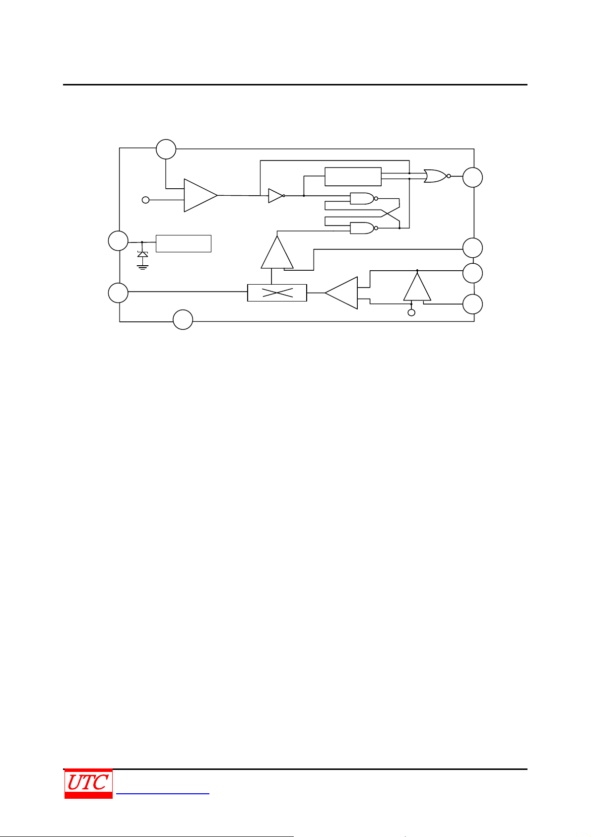
BLOCK DIAGRAM
I
DET
5
LINEAR INTEGRATED CIRCUIT
V
V
I(M 1)
CC
8
3
1.3V
(∆200mV)
+
UVNL
6
GND
Self-Starter
-
C
OMP
MULT
-
+
OP-AMP
+
-
V
REF
(2.5V )
-
+
V
OUT
7
4
V
CS
V
COMP
2
V
IN
1
UNISONIC TECHNOLOGIES CO., LTD
www.unisonic.com.tw
QW-R114-002.D
2 of 5
Page 3

7524
LINEAR INTEGRATED CIRCUIT
ABSOLUTE MAXIMUM RATINGS
(Ta = 25℃)
PARAMETER SYMBOL RATINGS UNIT
Supply Voltage VCC 20 V
Peak Driver Output Current I
Detect Clamping Diode Current I
Output Clamping Diode Current I
O(PEAK)
10 mA
DET
10 mA
O(CD)
500 mA
Junction Temperature TJ +125 °C
Operating Temperature T
Storage Temperature T
-20~+85 °C
OPR
-40~+150 °C
STG
Note 1. Absolute maximum ratings are those values beyond which the device could be permanently damaged.
Absolute maximum ratings are stress ratings only and functional device operation is not implied.
2. The device is guaranteed to meet performance specification within 0℃~+70℃ operating temperature range
and assured by design from -20℃~+85℃.
ELECTRICAL CHARACTERISTICS
(Ta = 25℃, All voltage referenced to GND unless otherwise
specified)
PARAMETER SYMBOL TEST CONDITIONS MIN TYP MAX UNIT
Under Voltage Lockout Section
Start Threshold Voltage V
UV lockout Hysteresis V
THR(ST)
HYS(UV)
9.2 10 10.8 V
1.8 2.0 2.2 V
Supply Zener Voltage VZ 17 V
Supply Current Section
Start-up Supply Current Istart VCC<V
0.25 0.5 mA
I(THR)
Operating Supply Current ICC VCC=12V,No load 6 12 mA
Dynamic Operating Current I
Reference Section (Note 1)
Reference Voltage V
Line Regulation
Load Regulation
ΔV
ΔV
CC(D)
C
=1000pF
GS
2.45 2.5 2.55 V
REF
OUT
OUT
12V< V
0< I
<16V 0.1 10 mV
CC
<2mA 0.1 10 mV
REF
CC
10 20 mA
V
=12V,f=50KHZ,
Temperature Stability STT 20 mV
Error Amplifier Section
Input Offset Voltage V
Input Bias Current I
-15 15 mV
I(OFF)
-1 -0.1 1 µA
I(BIAS)
Large Signal Open Loop gain Gv 60 100 dB
Power Supply Rejection Ratio RR 60 86 dB
I
2 mA
Output Current
Output Voltage range V
SOURCE
I
-2 mA
SINK
1.2 4 V
O(P)
Unity Gain Bandwidth UBW 1.0 MHZ
Phase Margin MPH 57 °C
Multiplier Section
M1 Input Voltage Range V
M2 Input Voltage Range V
Input Bias Current I
Multiplier Gain (Note2) Gv V
0 2 V
I(M1)
V
I(M2)
-2 -0.5 2 µA
I(BIAS)
I(M1)
=0.5V,V
=3V 0.8 /V
I(M2)
V
REF
+1 V
REF
Multiplier Gain Stability STT -0.2 %/°C
Current Detect Section
Input Voltage Threshold V
Hysteresis V
1.0 1.3 1.6 V
I(THR)
200 mV
HYS
UNISONIC TECHNOLOGIES CO., LTD
www.unisonic.com.tw
QW-R114-002.D
3 of 5
Page 4

7524
LINEAR INTEGRATED CIRCUIT
ELECTRICAL CHARACTERISTICS(Cont.)
PARAMETER SYMBOL TEST CONDITIONS MIN TYP MAX UNIT
Input Low Clamp Voltage V
Input High Clamp Voltage V
Input Current IIN 0.8V<V
Input Clamp Diode Current I
Output Section
Output Voltage(High) V
Output Voltage(low) V
Rising Time tR CL=1000pF 100 200 ns
Failing Time tF CL=1000pF 90 200 ns
Self-Start Section
Self Starting Time tSS 12 µs
Note: 1.Reference can not be tested on the PKG
2.Gv=V
O(M)
/(V
I(M1)
*(V
I(M2)-VREF
))
IC(L)
IC(H)
V
I(CD)
O(H)
I
O(L)
I
DET
I
DET
DET
I
OUT
OUT
=0mA 0.95 V
=3mA 6.1 7.1 V
<6V 5 µA
DET
<0.9V,V
>6V 3 mA
DET
=-10mA,VCC=12V 7 9 V
=10mA,VCC=12V 0.8 1.8 V
UNISONIC TECHNOLOGIES CO., LTD
www.unisonic.com.tw
QW-R114-002.D
4 of 5
Page 5

7524
LINEAR INTEGRATED CIRCUIT
APPLICATION CIRCUIT
2A
H
TNR
F.G
N
C5
L1
C1
R3
R1 R4
C6 C7R2
C2
R5
D1
8
3
NTC
C3
C4
5
7
2
1
4
C9
6
BDI
R14
T1
D2
Q1
R6
C8
R13
R7
R8
R10
R11
C10 C11
R9
R12
VR1
Q3
R16
T2
D9
DIAC
R18
T2
D5
D3
R17
T2
Q2
D6
D4
R19
LAMP TUBE 1
L2
C12
D7 C14
L3
C13
LAMP TUBE 1
D8 C15
PART LIST
Resistor Capacitor Semiconductor Magnetics
R1 1.8M C1 0.1µF IC1 UTC 7524 T1 E1-25(PC30):P=70T,S=4T,Gap=0.5mm
R2 10K C2 0.1µF Q1 IRF830 T2 D15(GP-5):P=3T,S=13T
R3 100K C3 4700pF Q2 2SC5039 L1 EE-25(Iron Power),80mH
R4 3.3Ω C4 4700pF Q3 2SC5039 L2 EI-25(PC30):150T,Gap=0.4mm
R5 22K C5 0.1µF D1 1N4004
R7 2.2K C6 0.01µF D2 1N4937
R8 2.2M C7 100µF D3 1N4148
R9 150K C8 0.1µF D4 1N4148
R10 330Ω C9 3300pF D5 FR107
R11 0.75Ω C10 47µF/450V D6 FR107
R12 5.1K C11 0.1µF D7 FR107
R13 1M C12 3300pF D8 FR107
R14 390K C13 3300pF BD1 PBP204
R15 3.9M C14 0.01µF TNR 12G471
R16 5.1Ω C15 0.01µF DIAIC 32V
R17 27Ω
R18 5.1Ω
R19 27Ω
VR1 5K
NTC 10Ω
UTC assumes no responsibility for equipment failures that result from using products at values that
exceed, even momentarily, rated values (such as maximum ratings, operating condition ranges, or
other parameters) listed in products specifications of any and all UTC products described or contained
herein. UTC products are not designed for use in life support appliances, devices or systems where
malfunction of these products can be reasonably expected to result in personal injury. Reproduction in
whole or in part is prohibited without the prior written consent of the copyright owner. The information
presented in this document does not form part of any quotation or contract, is believed to be accurate
and reliable and may be changed without notice.
UNISONIC TECHNOLOGIES CO., LTD
www.unisonic.com.tw
QW-R114-002.D
5 of 5
 Loading...