

Page 1
74VHCT74A
DUAL D-TYPE FLIP FLOP WITH PRESET AND CLEAR
■ HIGH SPEED:
f
= 160 MHz (TYP.) at VCC = 5V
MAX
■ LOW POWER DISSIPATION:
I
= 2 µA (MAX.) at TA=25°C
CC
■ COMPA TIBLE WITH TTL OU TP U TS:
V
= 2V (MIN.), V
IH
■ POWER DOWN PROTECTION ON INPUTS
= 0.8V (MAX)
IL
& OUTPUTS
■ SYMMETRICAL OUTPUT IMPEDANCE:
|I
| = IOL = 8 mA (MIN)
OH
■ BALANCED PROPAGATION DELAYS:
t
≅ t
PLH
■ OPERATING VOLTAGE RANGE:
V
CC
■ PIN AND FUNCTION COMPATIBLE WITH
PHL
(OPR) = 4.5V to 5.5V
74 SERIES 74
■ IMPROVED LATCH-UP IMMUNITY
DESCRIPTION
The 74VHCT74A is an advanced high-speed
CMOS DUAL D-TYPE FLIP FLOP WITH PRESET
AND CLEAR fabricated with sub-micron silicon
gate and double-layer metal wiring C
2
MOS
technology.
A signal on the D INPUT is transferred to the Q
OUTPUT during the positive going transition of the
clock pulse.
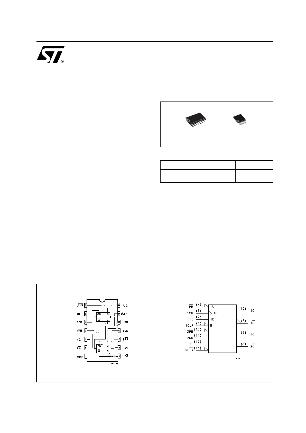
TSSOPSOP
ORDER CODES
PACKAGE TUBE T & R
SOP 74VHCT74AM 74VHCT74AMTR
TSSOP 74VHCT74ATTR
CLR
and PR are independent of the clock and
accomplished by a l ow setting on the app ropriate
input.
Power down protection is provided on all inputs
and outputs and 0 to 7V can be accepted on
inputs with no regard to the supply voltage. This
device can be us ed to interf ac e 5V to 3V since al l
inputs are equipped with TTL threshold.
All inputs and outputs are equipped with
protection circuits against stat ic discharge, giving
them 2KV ESD immunity and transient excess
voltage.
PIN CONNECTION AND IEC LOGIC SYMBOLS
1/11June 2001
Page 2
74VHCT74A
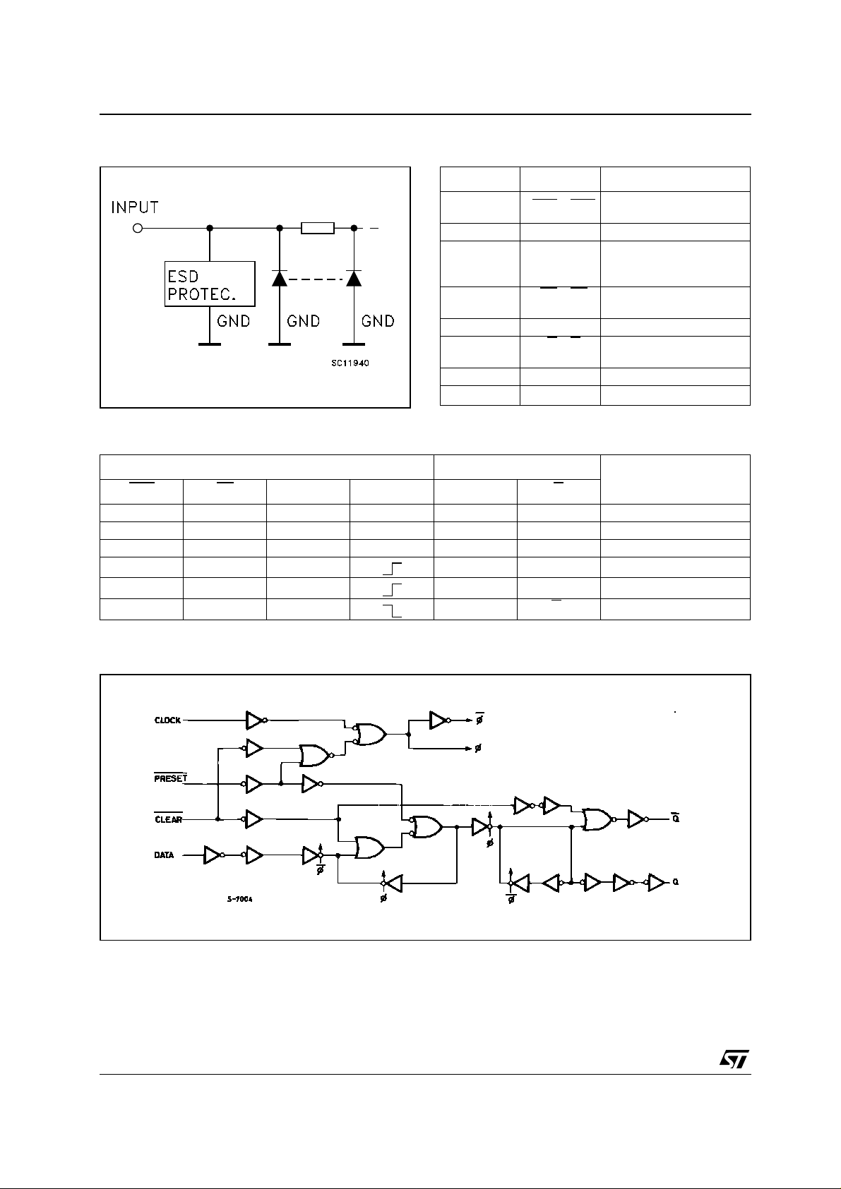
INPUT EQUIVALENT CIRCUIT PIN DESCRIPTION
PIN No SYMBOL NAME AND FUNCTION
1, 13 1CLR
2, 12 1D, 2D Data Inputs
3, 11 1CK, 2CK Clock Input
4, 10 1PR
5, 9 1Q, 2Q True Flip-Flop Outputs
6, 8 1Q
7 GND Ground (0V)
14 V
TRUTH TABLE
, 2CLR
, 2PR Asyncronous Set - Direct
, 2Q Complement Flip-Flop
CC
Asyncronous Reset Direct Input
(LOW to HIGH, Edge
Triggered)
Input
Outputs
Positive Supply Voltage
INPUTS OUTPUTS
CLR
PR DCKQ Q
L H X X L H CLEAR
H L X X H L PRESET
LLXXHH
HHL LH
HHH HL
HHX
X : Don’t Care
Q
n
Q
n
LOGIC DIAGRAM
FUNCTION
NO CHANGE
This log i c diagram has not be used to estimat e propagation del ays
2/11
Page 3
74VHCT74A
ABSOLUTE MAXIMUM RATINGS
Symbol Parameter Value Unit
V
V
V
V
I
I
OK
I
I
or I
CC
T
T
Absolute Maximum Ratings are those values beyond which damage to the device may occur. Functional operation under these conditions is
not implied
1) V
CC
2) High or Low State
RECOMMENDED OPERATING CONDITIONS
Symbol Parameter Value Unit
V
V
V
V
T
dt/dv
1) V
CC
2) High or Low State
3) VIN from 0.8V to 2V
Supply Voltage
CC
DC Input Voltage
I
DC Output Voltage (see note 1)
O
DC Output Voltage (see note 2) -0.5 to VCC + 0.5
O
DC Input Diode Current
IK
DC Output Diode Current
DC Output Current
O
DC VCC or Ground Current
GND
Storage Temperature
stg
Lead Temperature (10 sec)
L
= 0V
Supply Voltage
CC
Input Voltage
I
Output Voltage (see note 1)
O
Output Voltage (see note 2) 0 to V
O
Operating Temperature
op
Input Rise and Fall Time (see note 3) (V
= 0V
= 5.0 ± 0.5V)
CC
-0.5 to +7.0 V
-0.5 to +7.0 V
-0.5 to +7.0 V
- 20 mA
± 20 mA
± 25 mA
± 50 mA
-65 to +150 °C
300 °C
4.5 to 5.5 V
0 to 5.5 V
0 to 5.5 V
CC
-55 to 125 °C
0 to 20 ns/V
V
V
3/11
Page 4
74VHCT74A
DC SPECIFICATIONS
Symbol Parameter
V
V
V
V
I
I
OPD
High Level Input
IH
Voltage
Low Level Input
IL
Voltage
High Level Output
OH
Voltage
Low Level Output
OL
Voltage
I
Input Leakage
I
Current
Quiescent Supply
CC
Current
I
Additional Worst
CC
Case Supply
Current
Output Leakage
Current
Test Condition Value
T
= 25°C
V
CC
(V)
4.5 to
5.5
A
Min. Typ. Max. Min. Max. Min. Max.
222V
4.5 to
5.5
4.5
4.5
4.5
4.5
0 to
5.5
5.5
IO=-50 µA
I
=-8 mA
O
IO=50 µA
=8 mA
I
O
V
= 5.5V or GND
I
= VCC or GND
V
I
4.4 4.5 4.4 4.4
3.94 3.8 3.7
0.0 0.1 0.1 0.1
One Input at 3.4V,
other input at V
5.5
CC
or GND
= 5.5V
0
V
OUT
-40 to 85°C -55 to 125°C
Unit
0.8 0.8 0.8 V
V
0.36 0.44 0.55
V
± 0.1 ± 1.0 ± 1.0 µA
22020µA
1.35 1.5 1.5 mA
0.5 5.0 5.0 µA
AC ELECTRICAL CHARACTERISTICS (Input t
Test Condition Value
Symbol Parameter
t
Propagation Delay
PLH
t
t
t
t
REM
f
MAX
(*) Vol tage range is 5.0V ± 0.5V
Time CK to Q or Q
PHL
Propagation Delay
PLH
Time PR
PHL
Q or Q
t
CK Pulse Width
W
HIGH or LOW
t
PR or CLR Pulse
W
Width LOW
t
Setup Time D to CK
s
HIGH or LOW
t
Hold Time D to CK
h
HIGH or LOW
Removal Time
PR
Maximum Clock
Frequency
or CLR to
or CLR to CK
5.0
5.0
5.0
5.0
5.0
5.0
5.0
5.0
5.0
5.0
5.0
C
V
CC
(V)
L
(pF)
(*)
15 5.8 7.8 1.0 9.0 1.0 9.0
(*)
50 6.3 8.8 1.0 10.0 1.0 10.0
(*)
15 7.6 10.4 1.0 12.0 1.0 12.0
(*)
50 8.1 11.4 1.0 13.0 1.0 13.0
(*)
(*)
(*)
(*)
(*)
(*)
15 100 160 80 80
(*)
50 80 140 65 65
= tf = 3ns)
r
T
= 25°C
A
-40 to 85°C -55 to 125°C
Min. Typ. Max. Min. Max. Min. Max.
5.0 5.0 5.0 ns
5.0 5.0 5.0 ns
5.0 5.0 5.0 ns
0.0 0.0 0.0 ns
3.5 3.5 3.5 ns
Unit
ns
ns
MHz
4/11
Page 5

74VHCT74A
CAPACITIVE CHARACTERISTICS
Test Condition Value
= 25°C
Symbol Parameter
T
A
Min. Typ. Max. Min. Max. Min. Max.
C
C
Input Capacitance
IN
Power Dissipation
PD
Capacitance
6101010pF
21 pF
(note 1)
1) CPD is defined as the value of the IC’s internal equivalent capacitance which is calculated from the operating current consumption without
load. (Refer to Test Circuit). Average operating current can be obtained by the following equation. I
TEST CIRCUIT
-40 to 85°C -55 to 125°C
= CPD x VCC x fIN + ICC/2 (per gate)
CC(opr)
Unit
CL =15/50pF or equivalent (inc l udes jig and probe capacitanc e)
R
= Z
of pulse generator (typically 50Ω)
T
OUT
5/11
Page 6

74VHCT74A
WAVEFORM 1: PROPAGATION DELAYS, SETUP AND HOLD TIMES (f=1MHz; 50% duty cycle)
6/11
Page 7

74VHCT74A
WAVEFORM 2: PROPAGATION DELAYS (f=1MHz; 50% duty cycle)
WAVEFOR M 3: REMOVAL TI MES (f=1MHz; 50% duty cycl e)
7/11
Page 8

74VHCT74A
WAVEFORM 4: PULSE WIDTH
8/11
Page 9

SO-14 MECHANICAL DATA
74VHCT74A
DIM.
A 1.75 0.068
a1 0.1 0.2 0.003 0.007
a2 1.65 0.064
b 0.35 0.46 0.013 0.018
b1 0.19 0.25 0.007 0.010
C 0.5 0.019
c1 45° (typ.)
D 8.55 8.75 0.336 0.344
E 5.8 6.2 0.228 0.244
e 1.27 0.050
e3 7.62 0.300
F 3.8 4.0 0.149 0.157
G 4.6 5.3 0.181 0.208
L 0.5 1.27 0.019 0.050
M 0.68 0.026
S8° (max.)
MIN. TYP MAX. MIN. TYP. MAX.
mm. inch
PO13G
9/11
Page 10

74VHCT74A
TSSOP14 MECHANICAL DATA
mm. inch
DIM.
MIN. TYP MAX. MIN. TYP. MAX.
A 1.2 0.047
A1 0.05 0.15 0.002 0.004 0.006
A2 0.8 1 1.05 0.031 0.039 0.041
b 0.19 0.30 0.007 0.012
c 0.09 0.20 0.004 0.0089
D 4.9 5 5.1 0.193 0.197 0.201
E 6.2 6.4 6.6 0.244 0.252 0.260
E1 4.3 4.4 4.48 0.169 0.173 0.176
e 0.65 BSC 0.0256 BSC
K0° 8°0° 8°
L 0.45 0.60 0.75 0.018 0.024 0.030
A2
A
A1
b
e
c
K
L
E
D
E1
PIN 1 IDENTIFICATION
10/11
1
0080337D
Page 11

74VHCT74A
Information furnished is bel ieved to be accurate and reliable. However, STMicroe lectronics assumes no responsibility for the
consequences of use of such information nor for any infringement of patents or other rights of third parties which may result from
its use. No li cense is granted by implication or otherwise under any pat ent or patent rights of STMicroelec tronics. Specifications
mentioned in this publication ar e subject to change without notice. This publication supersedes and replaces all information
previously supplied. S TMicroelectronics products are not authorized for use as critica l components in life suppo rt devices or
systems without express written approval of STMicroelectronics.
Australi a - Brazil - China - Finland - Fra nce - Germany - Ho ng Kong - India - Italy - Japan - Mal aysia - Malta - Mo rocco
© The ST logo is a registered trademark of STMicroelectronics
© 2001 STM icroelectr o n ics - Printed in Italy - All Rights Reserved
STMicr o el ectronics GROU P OF COM P ANIES
Singapo re - Spain - Sweden - Switzerland - United K i ngdom
© http://www.st.com
11/11
 Loading...