

Page 1
74VHCT373A
OCTAL D-TYPE LATCH
WITH 3 STATE OUTPUT NON INVERTING
■ HIGHSPEED:t
■ LOW POWER DISSIPATION:
=4 µA (MAX.) at TA=25oC
I
CC
■ COMPATIBLEWITH TTLOUTPUTS:
=2V(MIN),VIL=0.8V(MAX)
V
IH
■ POWERDOWNPROTECTIONON INPUTS&
=6.4ns(TYP.)atVCC=5V
PD
OUTPUTS
■ SYMMETRICALOUTPUTIMPEDANCE:
|I
|=IOL=8 mA(MIN)
OH
■ BALANCEDPROPAGATIONDELAYS:
t
≅ t
PLH
PHL
■ OPERATINGVOLTAGERANGE:
(OPR)= 4.5Vto5.5V
V
CC
■ PINANDFUNCTIONCOMPATIBLEWITH
74SERIES373
■ IMPROVEDLATCH-UPIMMUNITY
■ LOWNOISE:V
= 0.9V(Max.)
OLP
DESCRIPTION
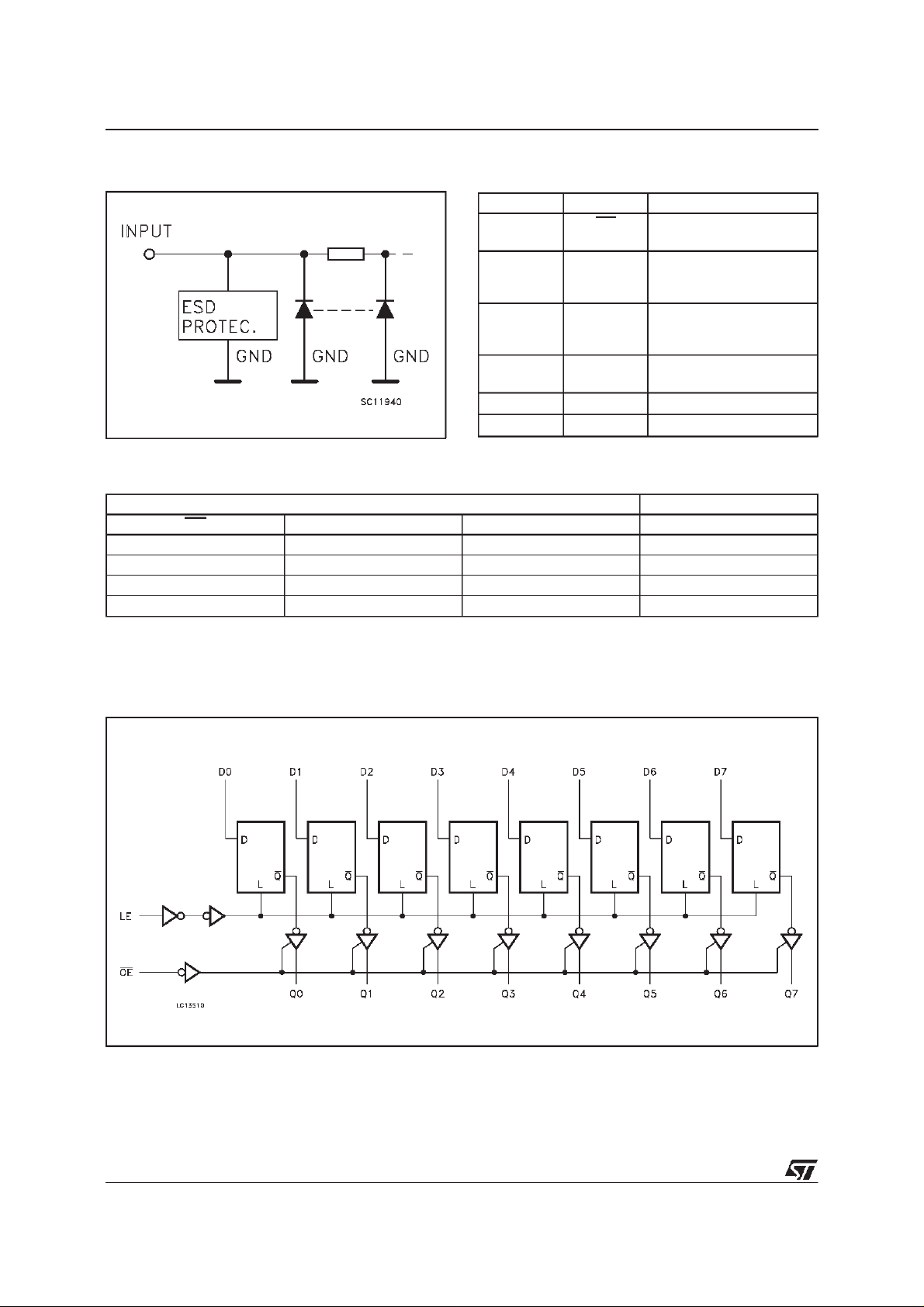
The 74VHCT373A is an advanced high-speed
CMOS OCTAL D-TYPE LATCH with 3 STATE
OUTPUT NON INVERTING fabricated with
sub-micron silicon gate and double-layer metal
wiringC
2
MOStechnology.
This 8 bit D-Type latch is controlled by a latch
enable input (LE) and an output enable input
M
(Micro Package)
(TSSOPPackage)
T
ORDERCODES :
74VHCT373AM 74VHCT373AT
(OE).
While the LE input is held at a high level, the Q
outputswill follow the data inputs precisely. When
the LE is taken low, the Q outputs will be latched
precisely at the logic level of D input data. While
the (OE) input is low, the 8 outputs will be in a
normal logic state (high or low logic level) and
while high level the outputs will be in a high
impedancestate.
Power down protection is provided on all inputs
and outputs and 0 to 7V can be accepted on
inputs with no regard to the supply voltage. This
devicecan be used to interface5V to 3V.
All inputs and outputs are equipped with
protection circuits against static discharge, giving
them 2KV ESD immunity and transient excess
voltage.
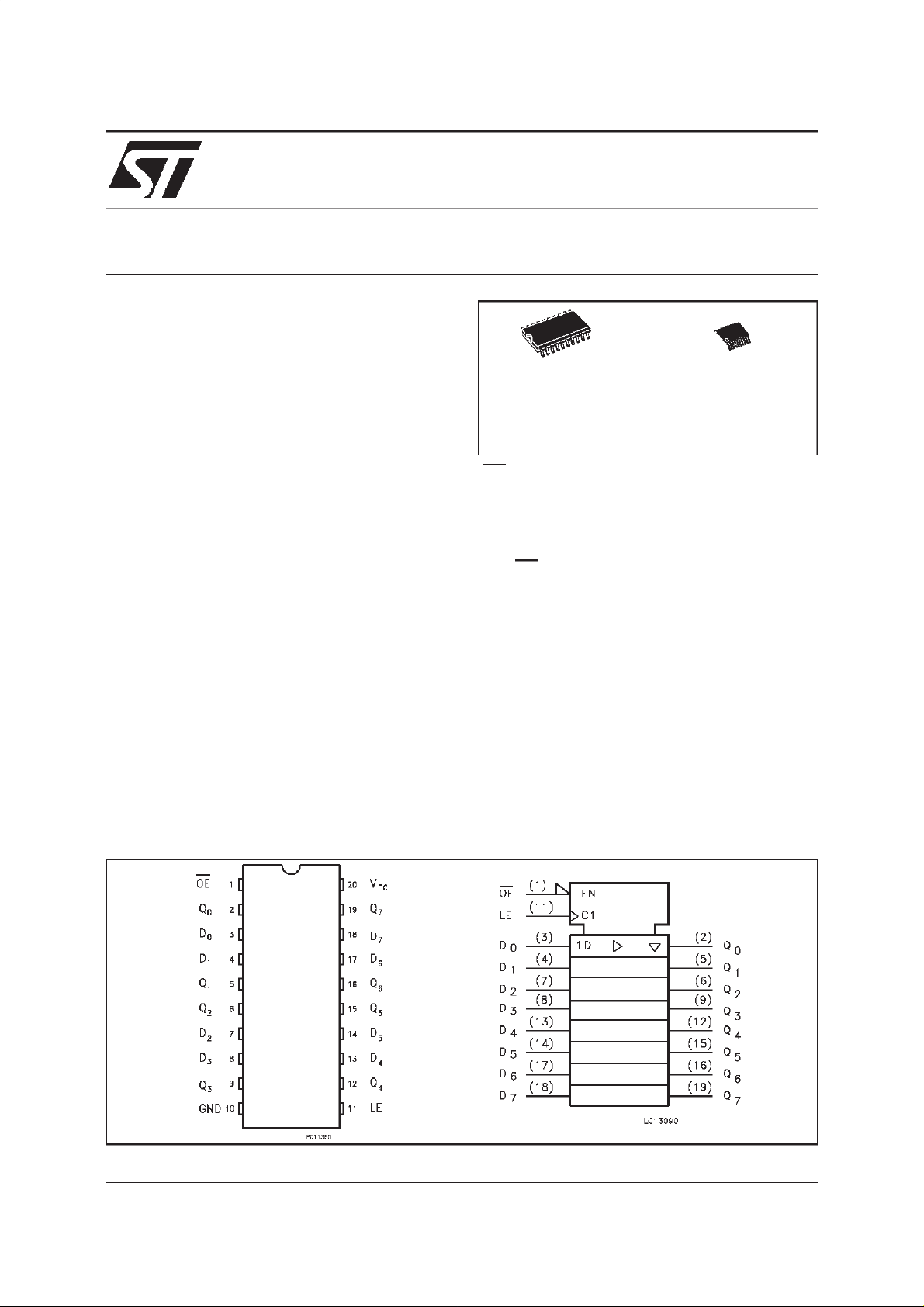
PIN CONNECTION AND IECLOGIC SYMBOLS
November 1999
1/10
Page 2
74VHCT373A
INPUT EQUIVALENTCIRCUIT PIN DESCRIPTION
PI N No SYMB OL NAME AND FUNCTION
1 OE 3 State Output Enable
2, 5, 6,
9, 12, 15,
16, 19
3, 4, 7,
8, 13, 14,
17, 18
11 LE Latch Enable
10 GND Ground (0V)
20 V
TRUTH TABLE
INPUTS OUTPUTS
OE LE D Q
HXXZ
L L X NO CHANGE *
LHLL
LHHH
X:DON’TCARE
Z:HIGHIMPEDANCE
*:QOUTPUTSARELATCHEDATTHETIMEWHENTHELEINPUTISTAKENLOWLOGICLEVEL.
Q0 to Q7 3 State Outputs
D0 to D7 Data Inputs
CC
Input (Active LOW)
Input
Positive Supply Voltage
LOGICDIAGRAM
2/10
Page 3
74VHCT373A
ABSOLUTE MAXIMUM RATINGS
Symb o l Paramet er Value U n i t
V
V
V
V
I
I
OK
I
or I
I
CC
T
T
AbsoluteMaximumRatingsarethosevaluesbeyond whichdamage tothedevicemayoccur.Functionaloperationunderthese conditionisnotimplied.
1)Output inOFFState
2)HighorLowState
RECOMMENDEDOPERATINGCONDITIONS
Symb o l Paramet er Value Unit
V
V
V
V
T
dt/dv
1)Output inOFFState
2)HighorLowState
from0.8Vto 2 V
3)V
IN
Supply Voltage -0.5 to +7.0 V
CC
DC Input Voltage -0.5 to +7.0 V
I
DC Output Voltage (see note 1) -0.5 to +7.0 V
O
DC Output Voltage (see note 2) -0.5 to VCC+ 0.5 V
O
DC Input Diode Current - 20 mA
IK
DC Output Diode Current
DC Output Current
O
DC VCCor Ground Current ± 50 mA
GND
Storage Temperature -65 to +150
stg
Lead Temperature (10 sec) 300
L
Supply Voltage 4.5 to 5.5 V
CC
Input Voltage 0 to 5.5 V
I
Output Voltage (see note 1) 0 to 5.5 V
O
Output Voltage (see note 2) 0 to V
O
Operating Temperature -40 to +85
op
Input Rise and Fall Time (see note 3) (V
=5.0±0.5V)
CC
20 mA
±
25 mA
±
CC
0 to 20 ns/V
o
C
o
C
V
o
C
3/10
Page 4

74VHCT373A
DC SPECIFICATIONS
Symb o l Para met er Test C o n ditio ns Val u e Uni t
T
=25oC -40 to 85oC
A
±0.25 ±2.5 µA
1.35 1.5 mA
V
V
V
V
I
I
∆I
I
OPD
V
CC
High Level Input
IH
(V)
4.5 to 5.5 2 2 V
Min. Typ. Max. Min. Max.
Voltage
Low Level Input
IL
4.5 to 5.5 0.8 0.8 V
Voltage
High Level Output
OH
Voltage
Low Level Output
OL
Voltage
High Impedance
OZ
Output Leakage
4.5 IO=-50 µA 4.4 4.5 4.4
4.5 I
=-8 mA 3.94 3.8
O
4.5 IO=50µA 0.0 0.1 0.1
4.5 I
4.5 to 5.5 VI=VIHor V
=8 mA 0.36 0.44
O
IL
VO= 0V to 5.5V
Current
Input Leakage Current 0 to5.5 VI= 5.5V or GND ±0.1 ±1.0 µA
I
I
Quiescent Supply
CC
5.5 VI=VCCorGND 4 40 µA
Current
Additional Worst Case
CC
Supply Current
5.5 One Input at 3.4V,
other inputat V
CC
or
GND
Output Leakage
0V
= 5.5V 0.5 5.0 µA
OUT
Current
V
V
AC ELECTRICAL CHARACTERISTICS
(Inputt
r=tf
=3 ns)
Symbol Parameter Test Condition Value Unit
t
Propagation Delay
PLH
Time LE to Q
t
PHL
Propagation Delay
t
PLH
t
Time D to Q
PHL
Output EnableTime 5.0
t
PZL
t
PZH
t
Output Disable Time 5.0
PLZ
t
PHZ
t
Pulse Width (LE)
w
V
(V)
5.0
5.0
5.0
5.0
5.0
5.0
CC
C
L
(pF)
(*)
15 5.4 12.3 1.0 13.5
(*)
(*)
(*)
(*)
(*)
(*)
(*)
50 6.0 13.3 1.0 14.5
15 6.4 8.5 1.0 9.5
50 7.1 9.5 1.0 10.5
15
50 6.9 11.9 1.0 13.5
R
L
=1KΩ
50 RL=1KΩ 6.7 11.2 1.0 12.0 ns
Min. Typ. Max. Min. Max.
=25oC -40 to 85oC
T
A
6.2 10.9 1.0 12.5
6.5 8..5 ns
ns
ns
ns
HIGH
Setup Time D to LE
t
s
5.0
(*)
1.5 1.5 ns
HIGH or LOW
Hold Time D toLE
t
h
5.0
(*)
3.5 3.5 ns
HIGH or LOW
t
t
(*) Voltagerangeis5V ± 0.5V
Note1:Parameterguaranteedbydesign.t
Output to Output Skew
OSLH
Time (note 1)
OSHL
soLH
5.0
=|t
pLHm-tpLHn
(*)
50 1.0 1.0 ns
|,t
soHL
=|t
pHLm-tpHLn
|
4/10
Page 5

74VHCT373A
CAPACITIVE CHARACTERISTICS
Symb o l Para met er Test C o n ditio ns Val u e Uni t
=25oC -40 to 85oC
T
A
Min. Typ. Max. Min. Max.
Input Capacitance 4 10 10
C
IN
C
Output Capacitance 9
OUT
Power Dissipation
C
PD
14 pF
Capacitance (note 1)
1)CPDisdefinedasthevalueoftheIC’sinternalequivalentcapacitance whichiscalculatedfromtheoperatingcurrentconsumption without load.(Referto
TestCircuit).Average operatingcurrentcanbeobtainedbythefollowingequation.I
(opr)= CPD• VCC• fIN+ICC/8(per Latch)
CC
DYNAMICSWITCHING CHARACTERISTICS
Symb o l Para met er Test C o n ditio ns Val u e Uni t
T
V
CC
(V)
V
V
V
Dynamic Low Voltage
OLP
Quiet Output (note 1, 2)
OLV
Dynamic High Voltage
IHD
5.0
5.0 2.0
C
L
=50pF
Min. Typ. Max. Min. Max.
Input (note 1, 3)
V
Dynamic Low Voltage
ILD
5.0 0.8
Input (note 1, 3)
1)Worst casepackage.
2)Maxnumberofoutputsdefinedas(n).Datainputsaredriven 0Vto3.0V,(n-1)outputsswitching andoneoutputatGND.
3)Maxnumberofdatainputs(n)switching.(n-1)switching0Vto3.0V. Inputsunder testswitching:3.0Vtothreshold (V
=25oC -40 to 85oC
A
0.6 0.9
-0.9 -0.6
),0Vtothreshold(V
ILD
),f=1MHz.
IHD
pF
pF
V
TESTCIRCUIT
TEST SWITCH
t
PLH,tPHL
t
PZL,tPLZ
t
PZH,tPHZ
CL= 15/50 pForequivalent (includes jig and probecapacitance)
=1KΩorequivalent
R
L=R1
R
ofpulsegenerator (typically50Ω)
T=ZOUT
Open
V
CC
GND
5/10
Page 6

74VHCT373A
WAVEFORM1: LE TO Qn PROPAGATIONDELAYS, LEMINIMUM PULSE WIDTH,
Dn TO LE SETUP AND HOLDTIMES(f=1MHz;50% dutycycle)
6/10
Page 7

74VHCT373A
WAVEFORM2: OUTPUT ENABLE AND DISABLE TIMES
(f=1MHz;50% duty cycle)
WAVEFORM3: PROPAGATIONDELAY TIME(f=1MHz; 50% dutycycle)
7/10
Page 8

74VHCT373A
SO-20 MECHANICALDATA
DIM.
MIN. TYP. MAX. MIN. TYP. MAX.
A 2.65 0.104
a1 0.10 0.20 0.004 0.007
a2 2.45 0.096
b 0.35 0.49 0.013 0.019
b1 0.23 0.32 0.009 0.012
C 0.50 0.020
c1 45 (typ.)
D 12.60 13.00 0.496 0.512
E 10.00 10.65 0.393 0.419
e 1.27 0.050
e3 11.43 0.450
F 7.40 7.60 0.291 0.299
L 0.50 1.27 0.19 0.050
M 0.75 0.029
S 8 (max.)
mm inch
8/10
P013L
Page 9

TSSOP20 MECHANICAL DATA
74VHCT373A
DIM.
mm inch
MIN. TYP. MAX. MIN. TYP. MAX.
A 1.1 0.433
A1 0.05 0.10 0.15 0.002 0.004 0.006
A2 0.85 0.9 0.95 0.335 0.354 0.374
b 0.19 0.30 0.0075 0.0118
c 0.09 0.2 0.0035 0.0079
D 6.4 6.5 6.6 0.252 0.256 0.260
E 6.25 6.4 6.5 0.246 0.252 0.256
E1 4.3 4.4 4.48 0.169 0.173 0.176
e 0.65 BSC 0.0256 BSC
K0
o
o
4
o
8
o
0
o
4
L 0.50 0.60 0.70 0.020 0.024 0.028
o
8
A2
A
A1
PIN 1 IDENTIFICATION
b
e
K
c
L
E
D
E1
1
9/10
Page 10

74VHCT373A
Information furnished isbelieved to be accurate andreliable.However, STMicroelectronics assumes no responsibility for the consequences
of use of such information nor for any infringement of patents or other rights of third parties which may result from its use. No license is
granted by implication or otherwise under any patent or patent rights of STMicroelectronics. Specification mentioned in this publication are
subject tochange without notice. This publication supersedes andreplaces all informationpreviously supplied. STMicroelectronics products
are not authorized for use as critical components in lifesupport devices or systems withoutexpress written approval of STMicroelectronics.
The ST logo is a registered trademark of STMicroelectronics
1999 STMicroelectronics – Printedin Italy– All Rights Reserved
STMicroelectronics GROUP OF COMPANIES
Australia - Brazil- China - Finland - France -Germany - Hong Kong - India - Italy - Japan- Malaysia - Malta - Morocco
Singapore - Spain- Sweden- Switzerland - United Kingdom - U.S.A.
http://www.st.com
.
10/10
 Loading...