

Page 1

74VHCT240A
OCTAL BUS BUFFER
WITH 3 STATE OUTPUTS (INVERTED)
■ HIGHSPEED:t
■ LOW POWER DISSIPATION:
=4 µA (MAX.)at TA=25oC
I
CC
■ COMPATIBLEWITH TTLOUTPUTS:
=2V(MIN),VIL=0.8V(MAX)
V
IH
■ POWERDOWNPROTECTIONON INPUTS&
=5ns (TYP.)atVCC=5V
PD
OUTPUTS
■ SYMMETRICALOUTPUT IMPEDANCE:
|I
|=IOL=8 mA(MIN)
OH
■ BALANCEDPROPAGATIONDELAYS:
t
≅ t
PLH
PHL
■ OPERATINGVOLTAGERANGE:
(OPR)= 4.5Vto 5.5V
V
CC
■ PINANDFUNCTION COMPATIBLEWITH
74SERIES 240
■ IMPROVEDLATCH-UP IMMUNITY
■ LOWNOISE:V
= 0.9V(Max.)
OLP
DESCRIPTION
The 74VHCT240A is an advanced high-speed
CMOS OCTAL BUS BUFFER (3-STATE)
fabricated with sub-micron silicon gate and
double-layermetal wiringC
2
MOS technology.
M
(Micro Package)
(TSSOPPackage)
T
ORDERCODES :
74VHCT240AM 74VHCT240AT
G output enablegoverns four BUS BUFFERs.
This device is designed to be used with 3 state
memoryaddress drivers, etc.
Power down protection is provided on all inputs
and outputs and 0 to 7V can be accepted on
inputs with no regard to the supply voltage. This
devicecan be used to interface5V to 3V.
All inputs and outputs are equipped with
protection circuits against static discharge, giving
them 2KV ESD immunity and transient excess
voltage.
PIN CONNECTION AND IEC LOGIC SYMBOLS
August 1999
1/8
Page 2
74VHCT240A
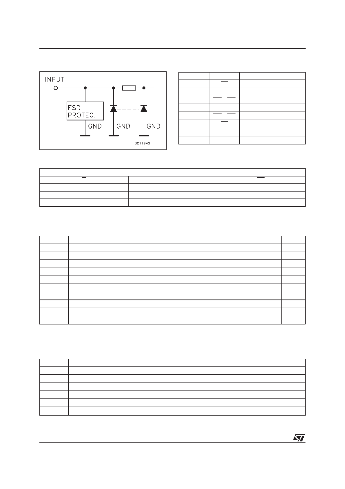
INPUT EQUIVALENTCIRCUIT
TRUTH TABLE
INPUT OUTPU T
GAnYn
LLH
LHL
HXZ
X:”H” or”L”
Z:Highimpedance
ABSOLUTE MAXIMUM RATINGS
PIN DESCRIPTION
PI N No SYM BO L NAM E AN D F UNCT I ON
1 1G Output Enable Input
2,4,6,8 1A1to1A4 Data Inputs
9,7,5,3 2Y1to2Y4 Data Outputs
11,13,15,17 2A1to2A4 Data Inputs
18,16,14,12 1Y1to1Y4 Data Outputs
19 2G Output Enable Input
10 GND Ground (0V)
20 V
Positive Supply Voltage
CC
Symb o l Para met er Value U n i t
V
V
V
V
I
I
OK
I
orI
I
CC
T
T
AbsoluteMaximum Ratingsarethosevaluesbeyond whichdamagetothedevicemayoccur. Functional operationunderthese condition isnotimplied.
1)Outputin OFFState
2)HighorLowState
Supply Voltage -0.5to+7.0 V
CC
DC Input Voltage -0.5to+7.0 V
I
DC Output Voltage (see note 1) -0.5to+7.0 V
O
DC Output Voltage (see note 2) -0.5toVCC+0.5 V
O
DC Input Diode Current -20 mA
IK
DC Output Diode Current
DC Output Current ±25 mA
O
DC VCCor Ground Current ±50 mA
GND
Storage Temperature -65to+150
stg
Lead Temperature (10 sec) 300
L
20 mA
±
o
C
o
C
RECOMMENDEDOPERATINGCONDITIONS
Symb o l Para met er Value Unit
V
V
V
V
T
dt/dv
1)Outputin OFFState
2)HighorLowState
3)V
from0.8Vto 2V
IN
2/8
Supply Voltage 4.5to5.5 V
CC
Input Voltage 0to5.5 V
I
Output Voltage (see note 1) 0to5.5 V
O
Output Voltage (see note 2) 0toV
O
Operating Temperature -40to+85
op
Input Rise and Fall Time (see note 3) (V
=5.0±0.5V)
CC
CC
0to20 ns/V
V
o
C
Page 3

74VHCT240A
DC SPECIFICATIONS
Symb o l Para met er Test Con dit io ns Val u e Un i t
T
V
CC
High Level Input
V
IH
(V)
4.5to5.5 2 2 V
Min. Typ. Max. Min. Max.
Voltage
Low Level Input
V
IL
4.5to5.5 0.8 0.8 V
Voltage
High Level Output
V
OH
Voltage
Low Level Output
V
OL
Voltage
High Impedance
I
OZ
Output Leakage
4.5 IO=-50µA4.44.5 4.4
4.5 I
=-8mA 3.94 3.8
O
4.5 IO=50µA 0.0 0.1 0.1
4.5 I
4.5to5.5 VI=VIHorV
=8mA 0.36 0.44
O
IL
VO=0Vto5.5V
Current
Input Leakage Current 0to5.5 VI=5.5Vor GND ±0.1 ±1.0 µA
I
I
Quiescent Supply
I
CC
5.5 VI=VCCorGND 2 20
Current
Additional Worst Case
∆I
CC
Supply Current
5.5 One Inputat 3.4V,
other input at V
CC
or
GND
I
Output Leakage
OPD
0V
=5.5V 0.5 5.0
OUT
Current
=25oC -40 t o 85oC
A
±0.25 ±2.5 µA
1.35 1.5 mA
µ
µ
V
V
A
A
AC ELECTRICAL CHARACTERISTICS (Input tr=tf=3 ns)
Symbol Parameter Test Co ndition Value Unit
t
Propagation Delay
PLH
t
Time
PHL
Output Disable Time 5.0
t
PLZ
t
PHZ
t
Output Enable Time 5.0
PZL
t
PZH
(*) Voltagerangeis5.0V± 0.5V
V
(V)
5.0
5.0
5.0
CC
C
L
(pF)
(*)
(*)
(*)
(*)
(*)
15 5.6 7.8 1.0 9.0
50 6.1 8.8 1.0 10.0
15 RL=1K
50 8.2 11.4 1.0 13.0
50 RL=1K
Min. Typ. Max. Min. Max.
Ω
Ω
=25oC -40 t o 85oC
T
A
7.7 10.4 1.0 12.0
8.8 11.4 1.0 13.0
ns
ns
ns
3/8
Page 4

74VHCT240A
CAPACITIVE CHARACTERISTICS
Symb o l Para met er Test Con dit io ns Val u e Un i t
=25oC -40 t o 85oC
T
A
Min. Typ. Max. Min. Max.
Input Capacitance 4 10 10
C
IN
C
Output Capacitance 9
OUT
Power Dissipation
C
PD
19 pF
Capacitance (note 1)
1)CPDisdefinedasthevalueoftheIC’sinternalequivalent capacitance whichis calculated fromtheoperatingcurrentconsumption withoutload.(Referto
TestCircuit).Average operatingcurrent canbeobtainedbythefollowingequation.I
(opr)=CPD• VCC• fIN+ICC/8(per Circuit)
CC
DYNAMICSWITCHING CHARACTERISTICS
Symb o l Para met er Test Con dit io ns Val u e Un i t
T
V
CC
(V)
V
V
Dynamic Low Voltage
OLP
Quiet Output (note 1, 2)
OLV
Dynamic High Voltage
V
IHD
5.0
5.0 2.0
=50pF
C
L
Min. Typ. Max. Min. Max.
Input (note 1, 3)
Dynamic Low Voltage
V
ILD
5.0 0.8
Input (note 1, 3)
1)Worstcasepackage.
2)Maxnumber ofoutputsdefined as(n).Datainputs aredriven0Vto 5.0V,(n-1)outputs switching andoneoutput atGND.
3)Maxnumber ofdatainputs(n)switching.(n-1)switching0Vto5.0V. Inputsunder testswitching: 5.0Vtothreshold (V
=25oC -40 t o 85oC
A
0.9 1.1
-1.1 -0.9
),0Vtothreshold (V
ILD
),f=1MHz.
IHD
pF
pF
V
TESTCIRCUIT
TEST SWITCH
t
PLH,tPHL
t
PZL,tPLZ
t
PZH,tPHZ
CL= 15/50 pF or equivalent (includes jig and probe capacitance)
=1KΩorequivalent
R
L=R1
R
ofpulse generator (typically50Ω)
T=ZOUT
Open
V
CC
GND
4/8
Page 5

74VHCT240A
WAVEFORM 1: PROPAGATIONDELAYS
(f=1MHz;50% duty cycle)
WAVEFORM 2: OUTPUT ENABLE AND DISABLE TIME (f=1MHz; 50%duty cycle)
5/8
Page 6

74VHCT240A
SO-20 MECHANICAL DATA
DIM.
MIN. TYP. MAX. MIN. TYP. MAX.
A 2.65 0.104
a1 0.10 0.20 0.004 0.007
a2 2.45 0.096
b 0.35 0.49 0.013 0.019
b1 0.23 0.32 0.009 0.012
C 0.50 0.020
c1 45 (typ.)
D 12.60 13.00 0.496 0.512
E 10.00 10.65 0.393 0.419
e 1.27 0.050
e3 11.43 0.450
F 7.40 7.60 0.291 0.299
L 0.50 1.27 0.19 0.050
M 0.75 0.029
S 8 (max.)
mm inch
6/8
P013L
Page 7

TSSOP20 MECHANICAL DATA
74VHCT240A
DIM.
mm inch
MIN. TYP. MAX. MIN. TYP. MAX.
A 1.1 0.433
A1 0.05 0.10 0.15 0.002 0.004 0.006
A2 0.85 0.9 0.95 0.335 0.354 0.374
b 0.19 0.30 0.0075 0.0118
c 0.09 0.2 0.0035 0.0079
D 6.4 6.5 6.6 0.252 0.256 0.260
E 6.25 6.4 6.5 0.246 0.252 0.256
E1 4.3 4.4 4.48 0.169 0.173 0.176
e 0.65 BSC 0.0256 BSC
K0
o
o
4
o
8
o
0
o
4
L 0.50 0.60 0.70 0.020 0.024 0.028
o
8
A2
A
A1
PIN 1 IDENTIFICATION
b
e
K
c
L
E
D
E1
1
7/8
Page 8

74VHCT240A
Information furnished is believed to beaccurate and reliable. However, STMicroelectronics assumes no responsibility forthe consequences
of use of such information nor for any infringement of patents or other rights of third parties which may result from its use. No license is
granted by implication or otherwise under any patent or patent rights of STMicroelectronics. Specification mentioned in this publication are
subject tochange without notice. Thispublication supersedes and replaces all information previously supplied. STMicroelectronics products
are not authorized for use as critical components in life support devices or systems without express written approval of STMicroelectronics.
The ST logo is a trademark of STMicroelectronics
1999 STMicroelectronics – Printed in Italy – All Rights Reserved
STMicroelectronics GROUP OF COMPANIES
Australia - Brazil - Canada - China - France - Germany - Italy - Japan - Korea - Malaysia - Malta - Mexico -Morocco - The Netherlands -
Singapore - Spain - Sweden - Switzerland - Taiwan - Thailand - UnitedKingdom - U.S.A.
http://www.st.com
.
8/8
 Loading...