

Datasheet 74VHCT138AMTC, 74VHCT138AM, 74VHCT138ACW, 74VHCT138ASJX, 74VHCT138ASJ Datasheet (Fairchild Semiconductor)
...Page 1
June 1997
Revised April 1999
74VHCT138A 3-to-8 Decoder/Demultiplexer
© 1999 Fairchild Semiconductor Corporation DS500014.prf www.fairchildsemi.com
74VHCT138A
3-to-8 Decoder/Demultiplexer
General Description
The VHCT138A is an ad vanced high speed C MOS 3-to-8
DECODER fabricated with silic on gate CMOS technology.
It achieves the high speed operation similar to equivalent
Bipolar Schottky TTL while maintaining the CMOS low
power dissipation.
When the device is enab led, 3 Binary Select inputs ( A
0
, A
1
and A2) determine which one of the outputs (O0–O7) will go
LOW. When enable input E
3
is held LOW or either E1 or E
2
is held HIGH, decoding function is inhib ited and all outputs
go HIGH. E
3
, E1 and E2 inputs are provided to ease cas-
cade connection and for use as an address decoder f or
memory systems. Protection circuit s ensure that 0V to 7V
can be applied to the input pins without r egard to the sup-
ply voltage and to the output pins with V
CC
= 0V. These cir-
cuits prevent device destruction due to m isma tche d s upp l y
and input/output voltages. This device can be used to interface 3V to 5V systems and two supply system s such as
battery backup.
Features
■ High Speed: tPD = 7.6 ns (typ) at VCC = 5V
■ Low power dissipation: I
CC
= 4 µA (max.) at TA = 25°C
■ Power down protection is provided on all inputs and
outputs
■ Pin and function compatible with 74HCT138
Ordering Code:
Surface mount pack ages are also available on Tape and Reel. Specify by appending the s uffix let te r “X” to the ordering code.
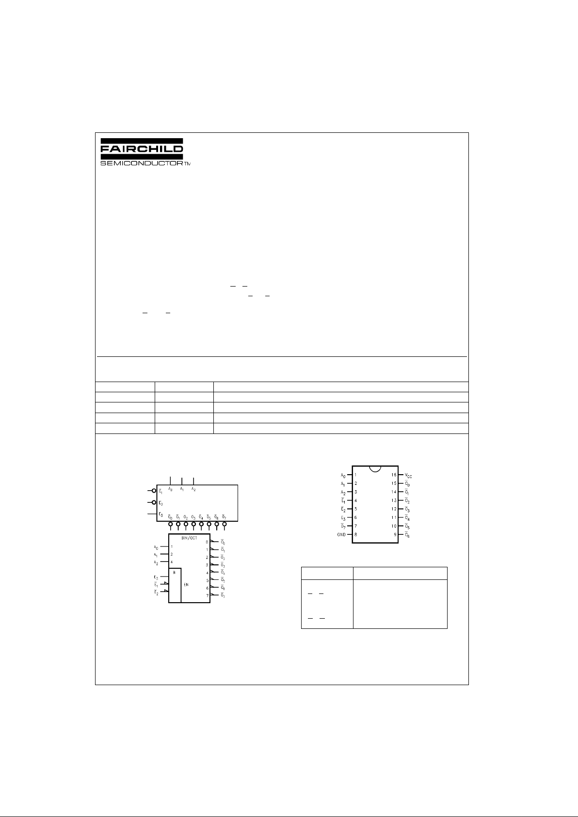
Logic Symbols
IEEE/IEC
Connection Diagram
Pin Descriptions
Order Number Package Number Package Description
74VHCT138AM M16A 16-Lead Small Outline Integrated Circuit (SOIC), JEDEC MS-012, 0.150 Narrow
74VHCT138ASJ M16D 16-Lead Small Outline Package (SOP), EIAJ TYPE II, 5.3mm Wide
74VHCT138AMTC MTC16 16-Lead Thin Shrink Small Outline Package (TSSOP), JEDEC MO-153, 4.4mm Wide
74VHCT138AN N16E 16-Lead Plastic Dual-In-Line Package (PDIP), JEDEC MS-001, 0.300 Wide
Pin Names Description
A
0–A2
Address Inputs
E
1–E2
Enable Inputs
E
3
Enable Input
O
0–O7
Outputs
Page 2
www.fairchildsemi.com 2
74VHCT138A
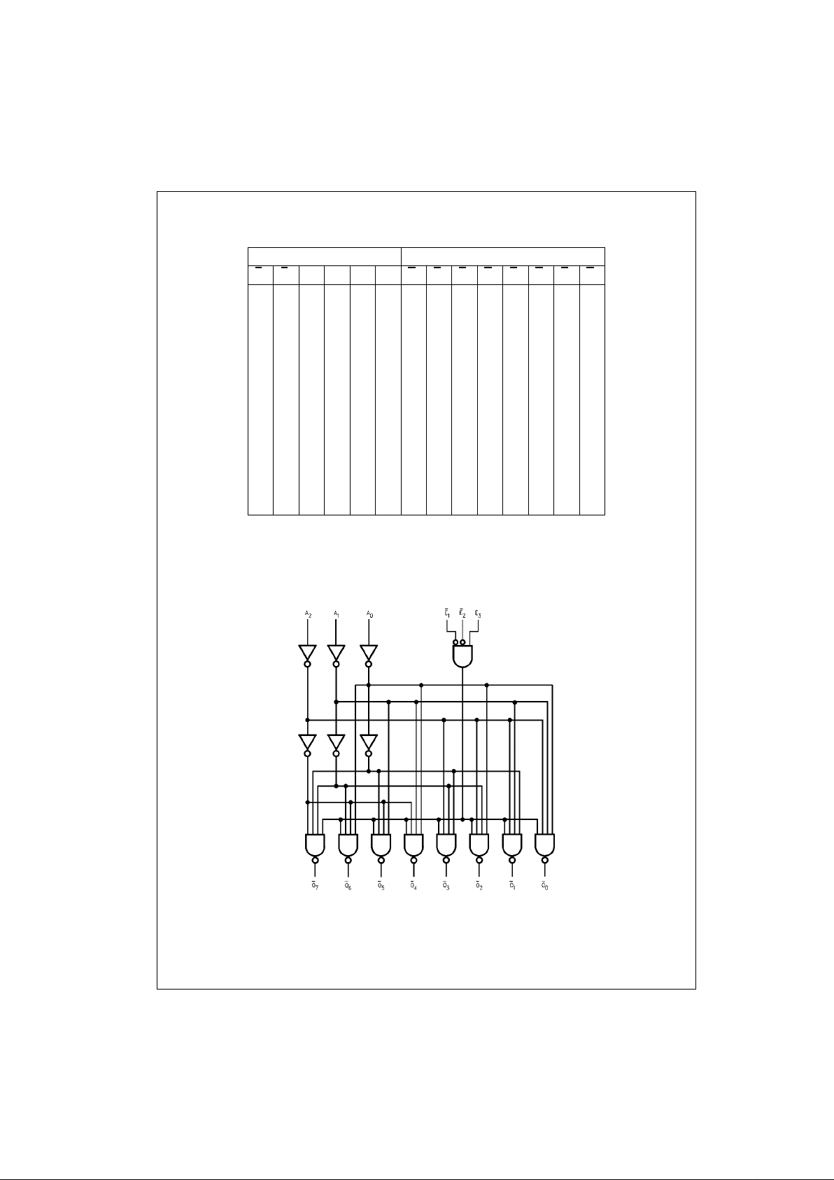
Truth Table
H = HIGH Voltage Level
L = LOW Voltage Level
X = Immaterial
Logic Diagram
Please note that this diagram is provided on ly fo r th e understanding of logic operations and should not be used to est im at e propagation delays.
Inputs Outputs
E
1E2E3A0A1A2O0O1O2O3O4O5O6O7
HXXXXXHHHHHHHH
XHXXXXHHHHHHHH
XXLXXXHHHHHHHH
LLHLLLLHHHHHHH
LLHHLLHLHHHHHH
LLHLHLHHLHHHHH
LLHHHLHHHLHHHH
LLHLLHHHHHLHHH
LLHHLHHHHHHLHH
LLHLHHHHHHHHLH
LLHHHHHHHHHHHL
Page 3
3 www.fairchildsemi.com
74VHCT138A
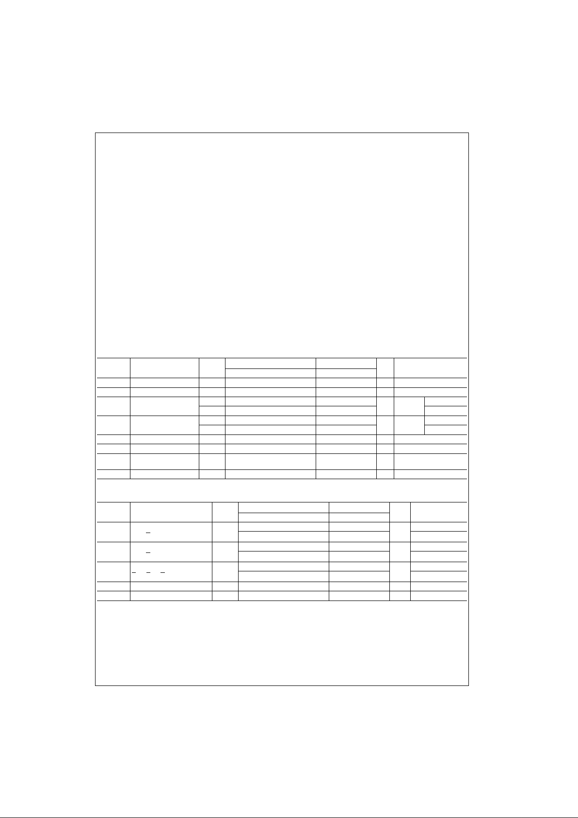
Absolute Maximum Ratings(Note 1) Recommended Operating
Conditions
(Note 5)
Note 1: Absolute Maximum Ratings are valu es beyond whic h the device
may be damaged or ha ve its useful life impaire d. The datab ook specifications should be met, without exception, to ensure that the system design is
reliable over its p ower supp ly, temperature, and o utput/input loading variables. Fairchild does not recommend operation outside databook specifications.
Note 2: V
CC
= 0V.
Note 3: HIGH or LOW state. I
OUT
absolute maximum rating must be
observed.
Note 4: V
OUT
<GND, V
OUT
> VCC (Outputs Active).
Note 5: Unused inputs must be held HIGH or LOW. They may not float.
DC Electrical Characteristics
AC Electrical Characteristics
Note 6: CPD is defined as the value of the internal equi v alent capacitance w hic h is calculated from t he operating current c ons umption without load. Av erage
operating current ca n be obtained by the equ at ion: I
CC
(opr.) = CPD * VCC * fIN + ICC.
Supply Voltage (VCC) −0.5V to +7.0V
DC Input Voltage (V
IN
) −0.5V to +7.0V
DC Output Voltage (V
OUT
)
(Note 2) −0.5V to 7.0V
(Note 3) −0.5V to V
CC
+ 0.5V
Input Diode Current (I
IK
) −20 mA
Output Diode Current (I
OK
)
(Note 4) ±20 mA
DC Output Current (I
OUT
) ±25 mA
DC V
CC
/GND Current (ICC) ±75 mA
Storage Temperature (T
STG
) −65°C to +150°C
Lead Temperature (T
L
)
(Soldering, 10 seconds) 260°C
Supply Voltage (V
CC
) 4.5V to +5.5V
Input Voltage (V
IN
)0V to +5.5V
Output Voltage (V
OUT
)
(Note 3) 0V to V
CC
(Note 2) 0V to 5.5V
Operating Temperature (T
OPR
) −40°C to +85°C
Input Rise and Fall Time (t
r
, tf)
V
CC
= 5.0V ± 0.5V 0 ∼ 20 ns/V
Symbol Parameter
V
CC
(V)
TA = 25°CT
A
= −40°C to +85°C
Units Conditions
Min Typ Max Min Max
V
IH
HIGH Level Input Voltage 4.5 − 5.5 2.0 2.0 V
V
IL
LOW Level Input Voltage 4.5 − 5.5 0.8 0.8 V
V
OH
HIGH Level 4.5 4.4 4.5 4.4
V
VIN = VIH IOH = −50 µA
Output Voltage 4.5 3.94 3.80 or VILIOH = −8 mA
V
OL
LOW Level 4.5 0.0 0.1 0.1
V
VIN = VIH IOL = 50 µA
Output Voltage 4.5 0.36 0.44 or VILIOL = 8 mA
I
IN
Input Leakage Current 0 − 5.5 ±0.1 ±1.0 µAVIN = 5.5V or GND
I
CC
Quiescent Supply Current 5.5 4.0 20.0 µAVIN = VCC or GND
I
CCT
Maximum I
CC/Input
5.5 1.35 1.50 mA V
in
= 3.4V
other inputs = VCC or GND
I
OFF
Output Leakage Current 0 0.5 5.0 µAV
OUT
= 5.5V
Symbol Parameter
V
CC
(V)
TA = 25°CT
A
= −40°C to +85°C
Units Conditions
Min Typ Max Min Max
t
PLH
Propagation Delay 5.0 ± 0.5 7.6 10.4 1.0 12.0
ns
CL = 15 pF
t
PHL
An to O
n
8.111.41.013.0 CL = 50 pF
t
PLH
Propagation Delay 5.0 ± 0.5 6.6 9.1 1.0 10.5
ns
CL = 15 pF
t
PHL
E3 to O
n
7.1 10.1 1.0 11.5 CL = 50 pF
t
PLH
Propagation Delay 5.0 ± 0.5 7.0 9.6 1.0 11.0
ns
CL = 15 pF
t
PHL
E1 or E2 to O
n
7.5 10.6 1.0 12.0 CL = 50 pF
C
IN
Input Capacitance 4 10 10 pF VCC = Open
C
PD
Power Dissipation Capacitance 49 pF (Note 6)
Page 4
www.fairchildsemi.com 4
74VHCT138A
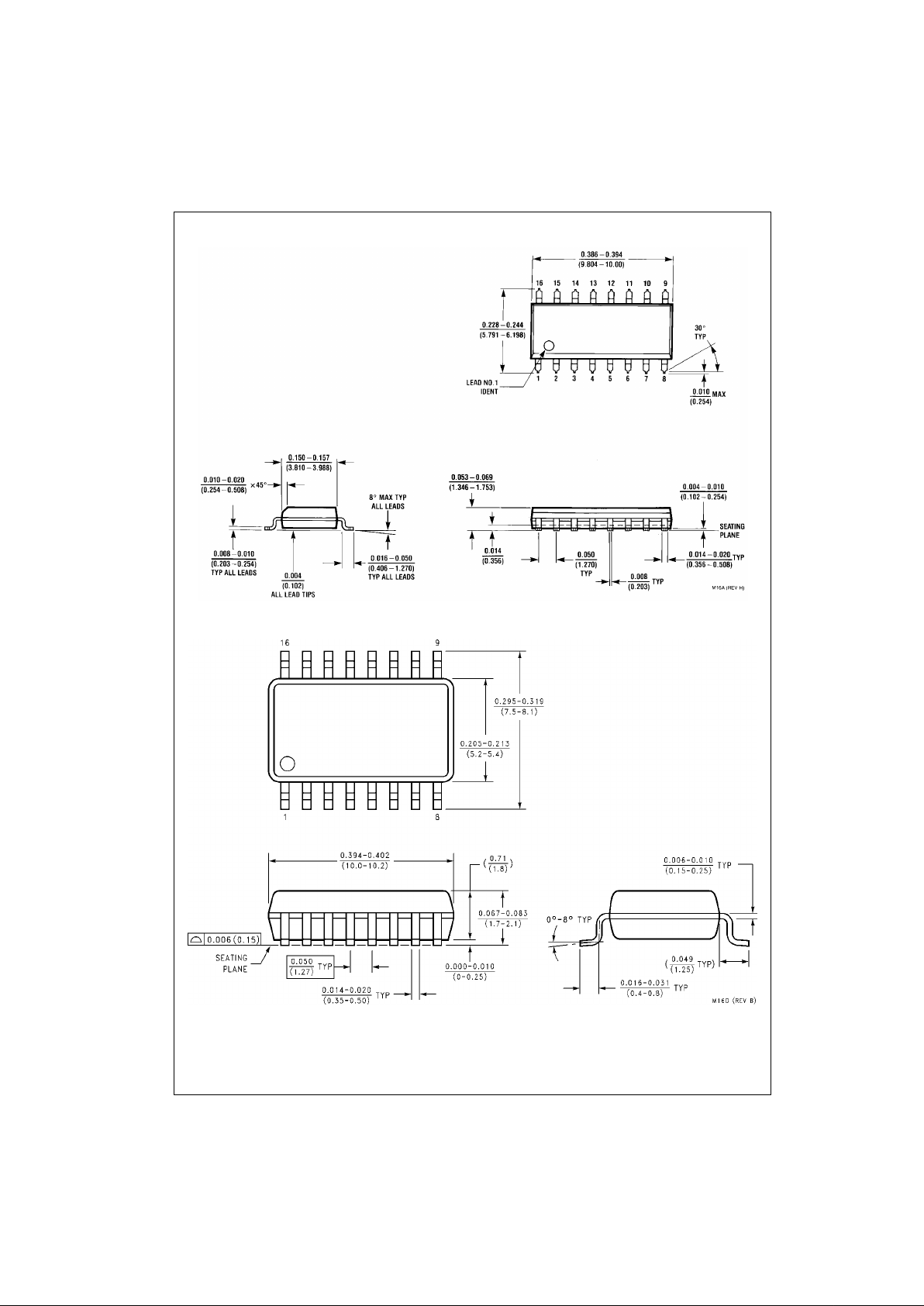
Physical Dimensions inches (millimeters) unless otherwise noted
16-Lead Small Outline Integrated Circuit (SOIC), JEDEC MS-012, 0.150 Narrow
Package Number M16A
16-Lead Small Outline Package (SOP), EIAJ TYPE II, 5.3mm Wide
Package Number M16D
Page 5
5 www.fairchildsemi.com
74VHCT138A
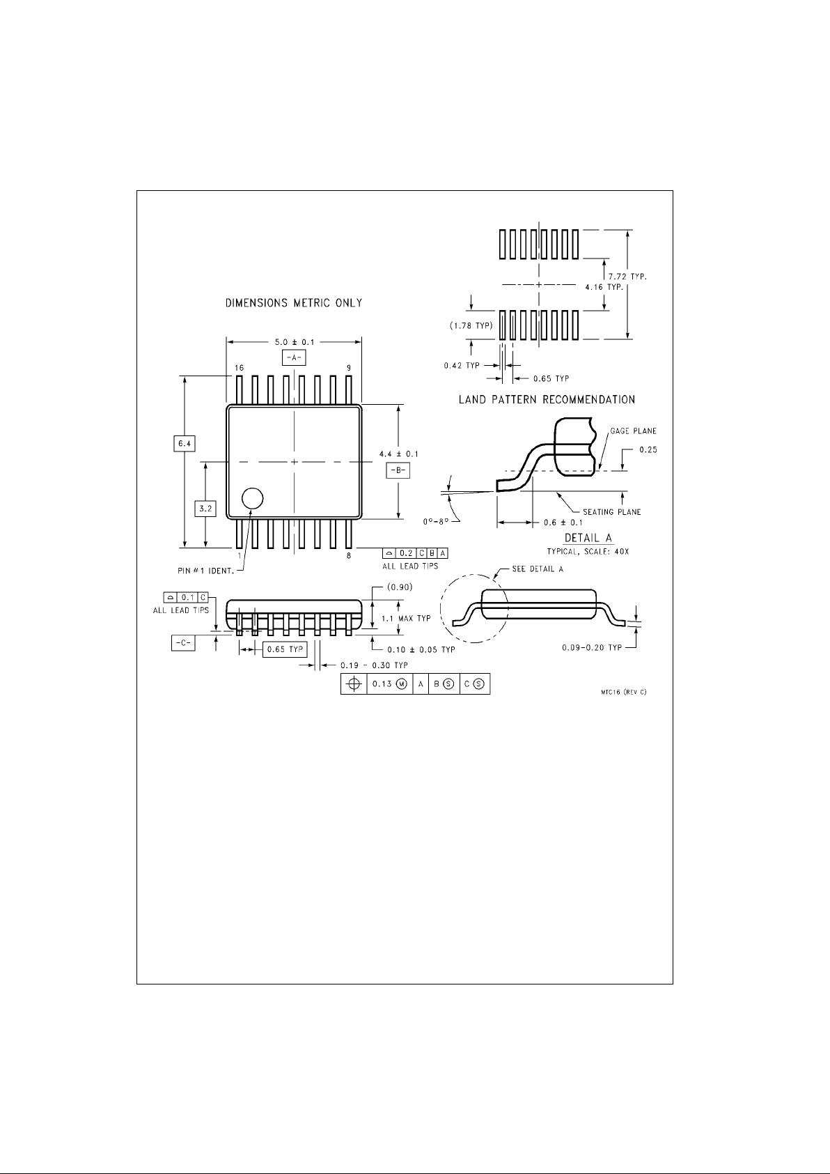
Physical Dimensions inches (millimeters) unless otherwise noted (Continued)
16-Lead Thin Shrink Small Outline Package (TSSOP), JEDEC MO-153, 4.4mm Wide
Package Number MTC16
Page 6
Fairchild does not assume any responsibility for use of any circuitry described, no circuit patent licenses are implied and Fairchild reserves the right at any time without notice to change said circuitry and specifications.
74VHCT138A 3-to-8 Decoder/Demultiplexer
LIFE SUPPORT POLICY
FAIRCHILD’S PRODUCTS ARE NOT AUTHORIZED FOR USE AS CRITICAL COMPONENTS IN LIFE SUPPORT
DEVICES OR SYSTEMS WITHOUT THE EXPRESS WRITTEN APPROVAL OF THE PRESIDENT OF FAIRCHILD
SEMICONDUCTOR CORPORATION. As used herein:
1. Life support devices or systems are devices or syste ms
which, (a) are intended for surgical implant into the
body, or (b) support or sustain life, and (c) whose failure
to perform when properly used in accordance with
instructions for use provided in the labeling, can be reasonably expected to result in a significant inju ry to the
user.
2. A critical component i n any compon ent of a lif e support
device or system whose failu re to perform can be reasonably expected to ca use the fa i lure of the life su pp ort
device or system, or to affect its safety or effectiveness.
www.fairchildsemi.com
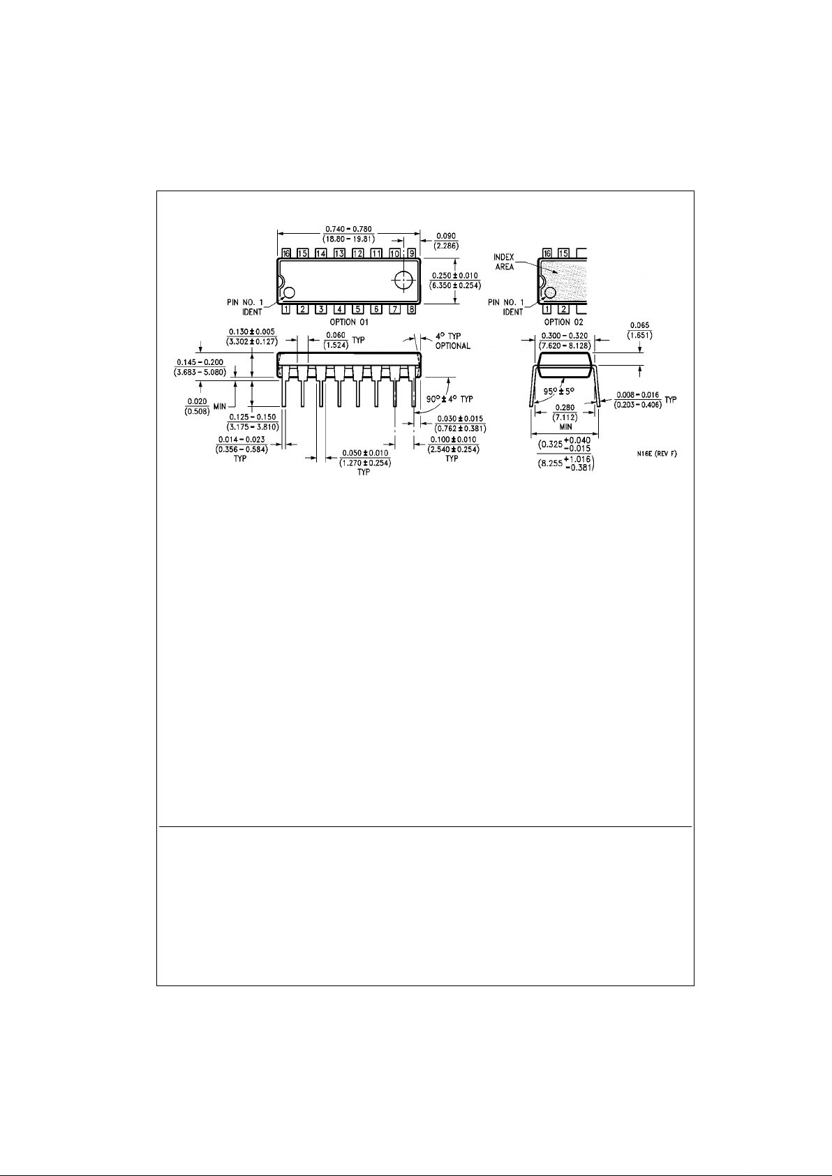
Physical Dimensions inches (millimeters) unless otherwise noted (Continued)
16-Lead Plastic Dual-In-Line Package (PDIP), JEDEC MS-001, 0.300 Wide
Package Number N16E
 Loading...