

Page 1

3 TO 8 LINE DECODER (INVERTING)
■ HIGH SPEED:t
■ LOW POW ERDISSIPATION:
=4 µA(M AX.)at TA=25oC
I
CC
■ COMPATIBLEWITHTTLOUTPUTS:
=2V(MIN),VIL=0.8V(MAX)
V
IH
■ POWERDOWNPROTECTIONON INPUTS&
OUTPUTS
■ SYMMETRICAL OUTPUTIMPEDANCE:
|I
|=IOL=8 mA(MIN)
OH
■ BALANCEDPROPAGATIONDELAYS:
t
≅ t
PLH
PHL
■ OPERATINGVOLTAGERAN GE:
(OPR)= 4.5V to 5.5V
V
CC
■ PINANDFUNCTIONCOMPATIBLEWITH
74SERIES138
■ IMPROVEDLATCH-UP IMMUNITY
■ LOWNOISE:V
DESCRIPTION
The 74VHCT138A is an advanced high-speed
CMOS 3 TO 8 LINE DECODER (INVERTING)
fabricated with sub-micron silicon gate and
double-layermetal wiringC
If the device is enabled,3 binary select inputs (A,
B and C) determine which one of the outputs will
go low. If enable input G1 is held low or either
=7.6ns (TYP.)atVCC=5V
PD
= 0.8V(Max.)
OLP
2
MOS technology.
74VHCT138A
PRELIMINARY DATA
SOP TSSOP
ORDER CODES
PACKAGE TUBE T & R
SOP 74VHCT138AM 74VHCT138AMTR
TSSOP 74VHCT138ATTR
G2A or G2B is heldhigh, the decoding function is
inhibitedand all the 8 outputsgo to high.
Three enable inputs are provided to ease
cascade connection and application of address
decodersfor memory systems.
Power down protection is provided on all inputs
and outputs and 0 to 7V can be accepted on
inputs with no regard to the supply voltage. This
devicecan be used tointerface5V to 3V.
All inputs and outputs are equipped with
protection circuits against static discharge, giving
them 2KV ESD immunity and transient excess
voltage.
PIN CONNECTION AND IEC LOGIC SYMBOLS
March 2000
1/8
Page 2
74VHCT138A
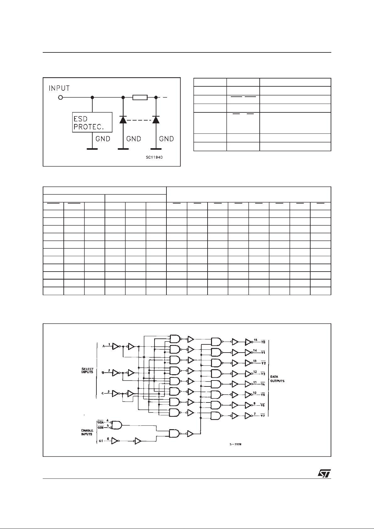
INPUT EQUIVALENTCIRCUIT
PIN DESCRIPTION
PI N No SYM BO L NAM E AND FU NCTION
1, 2, 3 A, B, C Address Inputs
4, 5 G2A, G2B Enable Inputs
6 G1 Enable Input
15, 14, 13,
12, 11, 10,
9, 7
8 GND Ground (0V)
16 V
Y0 to Y7 Outputs
CC
Positive Supply Voltage
TRUTH TABLE
INPUTS OUTPUTS
ENABLE SELECT
G2BG2AG1 C B A Y0Y1Y2Y3Y4Y5Y6Y7
XXLXXXHHHHHHHH
XHXXXXHHHHHHHH
HXXXXXHHHHHHHH
LLHLLLLHHHHHHH
LLHLLHHLHHHHHH
LLHLHLHHLHHHHH
LLHLHHHHHLHHHH
LLHHLLHHHHLHHH
LLHHLHHHHHHLHH
LLHHHLHHHHHHLH
LLHHHHHHHHHHHL
X:Don’tCare
LOGICDIAGRAM
Thislogicdiagram has notbe used toestimate propagation delays
2/8
Page 3

74VHCT138A
ABSOLUTE MAXIMUM RATINGS
Symb o l Para met er Value U n i t
V
V
V
V
I
I
OK
I
or I
I
CC
T
T
AbsoluteMaximumRatingsarethosevaluesbeyondwhichdamagetothedevice mayoccur. Functional operation under these condition isnotimplied.
1)V
=0
CC
2)High orLow State
RECOMMENDED OPERATINGCONDITIONS
Symb o l Para met er Value Unit
V
V
V
V
T
dt/dv
1)VCC=0
2)High orLow State
from0.8Vto 2 V
3)V
IN
Supply Voltage -0.5 to +7.0 V
CC
DC Input Voltage -0.5 to +7.0 V
I
DC Output Voltage (see note 1) -0.5 to +7.0 V
O
DC Output Voltage (see note 2) -0.5 to VCC+ 0.5 V
O
DC Input Diode Current - 20 mA
IK
DC Output Diode Current
DC Output Current
O
DC VCCor Ground Current ± 50 mA
GND
Storage Temperature -65 to +150
stg
Lead Temperature (10 sec) 300
L
Supply Voltage 4.5 to 5.5 V
CC
Input Voltage 0 to 5.5 V
I
Output Voltage (see note 1) 0 to 5.5 V
O
Output Voltage (see note 2) 0 to V
O
Operating Temperature -40 to +85
op
Input Rise and Fall Time (see note 3) (V
=5.0±0.5V)
CC
20 mA
±
25 mA
±
CC
0 to 20 ns/V
o
C
o
C
V
o
C
DC SPECIFICATIONS
Symb o l Para met er Test C o n ditions Val u e Uni t
T
=25oC -40 to 85oC
A
1.35 1.5 mA
µ
V
V
V
V
I
∆I
I
OPD
V
CC
High Level Input
IH
(V)
4.5 to 5.5 2 2 V
Min. Typ. Max. Min. Max.
Voltage
Low Level Input
IL
4.5 to 5.5 0.8 0.8 V
Voltage
High Level Output
OH
Voltage
Low Level Output
OL
Voltage
Input Leakage Current 0 to 5.5 VI= 5.5V or GND ±0.1 ±1.0 µA
I
I
Quiescent Supply
CC
4.5 IO=-50 µA 4.4 4.5 4.4
4.5 I
=-8 mA 3.94 3.8
O
4.5 IO=50 µ A 0.0 0.1 0.1
4.5 I
=8 mA 0.36 0.44
O
5.5 VI=VCCorGND 4 40
Current
Additional Worst Case
CC
Supply Current
5.5 One Input at 3.4V,
other input at V
CC
or
GND
Output Leakage
0V
= 5.5V 0.5 5.0 µA
OUT
Current
V
V
A
3/8
Page 4
74VHCT138A
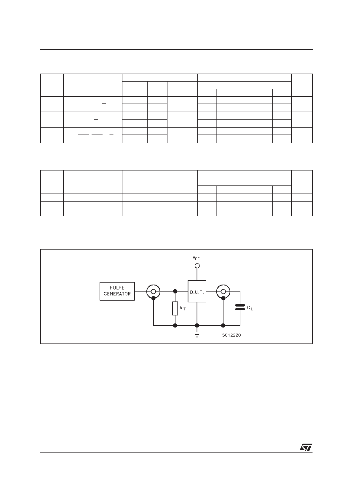
AC ELECTRICALCHARACTERISTICS
(Inputt
r=tf
=3 ns)
Symbol Parameter Test Condition Value Unit
t
Propagation Delay
PLH
t
Time A, B, C to Y
PHL
Propagation Delay
t
PLH
t
Time G1 toY
PHL
Propagation Delay
t
PLH
t
Time G2A, G2B to Y
PHL
(*) Voltagerangeis5V±0.5V
V
(V)
5.0
5.0
5.0
5.0
5.0
5.0
CC
C
L
(pF)
(*)
15 7.6 10.4 1.0 12.0
(*)
(*)
(*)
(*)
(*)
50 8.1 11.4 1.0 13.0
15 6.6 9.1 1.0 10.5
50 7.1 10.1 1.0 11.5
15 7.0 9.6 1.0 11.0
50 7.5 10.6 1.0 12.0
T
=25oC -40 to 85oC
A
Min. Typ. Max. Min. Max.
ns
ns
ns
CAPACITIVE CHARACTERISTICS
Symb o l Para met er Test C o n ditions Val u e Uni t
=25oC -40 to 85oC
T
A
Min. Typ. Max. Min. Max.
C
Input Capacitance 4 10 10
IN
Power Dissipation
C
PD
49 pF
Capacitance (note 1)
1)CPDisdefinedasthevalueoftheIC’sinternalequivalent capacitance whichiscalculated fromtheoperating currentconsumption withoutload.(Referto
Test Circuit).Averageoperatingcurrent canbeobtained bythefollowingequation.I
(opr)=CPD• VCC• fIN+I
CC
CC
pF
TESTCIRCUIT
CL= 15/50pF orequivalent (includes jigand probe capacitance)
R
ofpulsegenerator (typically50Ω)
T=ZOUT
4/8
Page 5
74VHCT138A
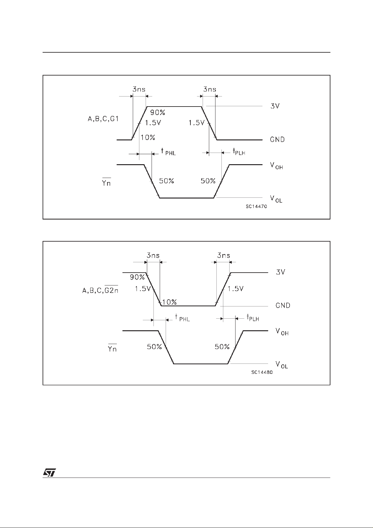
WAVEFORM 1: PROPAGATION DELAYS FOR INVERTING OUTPUTS(f=1MHz; 50% duty cycle)
WAVEFORM 2: PROPAGATION DELAYS FOR NON-INVERTINGOUTPUTS(f=1MHz; 50%dutycycle)
5/8
Page 6

74VHCT138A
SO-16 MECHANICALDATA
DIM.
MIN. TYP. MAX. MIN. TYP. MAX.
A 1.75 0.068
a1 0.1 0.2 0.004 0.007
a2 1.65 0.064
b 0.35 0.46 0.013 0.018
b1 0.19 0.25 0.007 0.010
C 0.5 0.019
c1 45 (typ.)
D 9.8 10 0.385 0.393
E 5.8 6.2 0.228 0.244
e 1.27 0.050
e3 8.89 0.350
F 3.8 4.0 0.149 0.157
G 4.6 5.3 0.181 0.208
L 0.5 1.27 0.019 0.050
M 0.62 0.024
S 8 (max.)
mm inch
6/8
P013H
Page 7
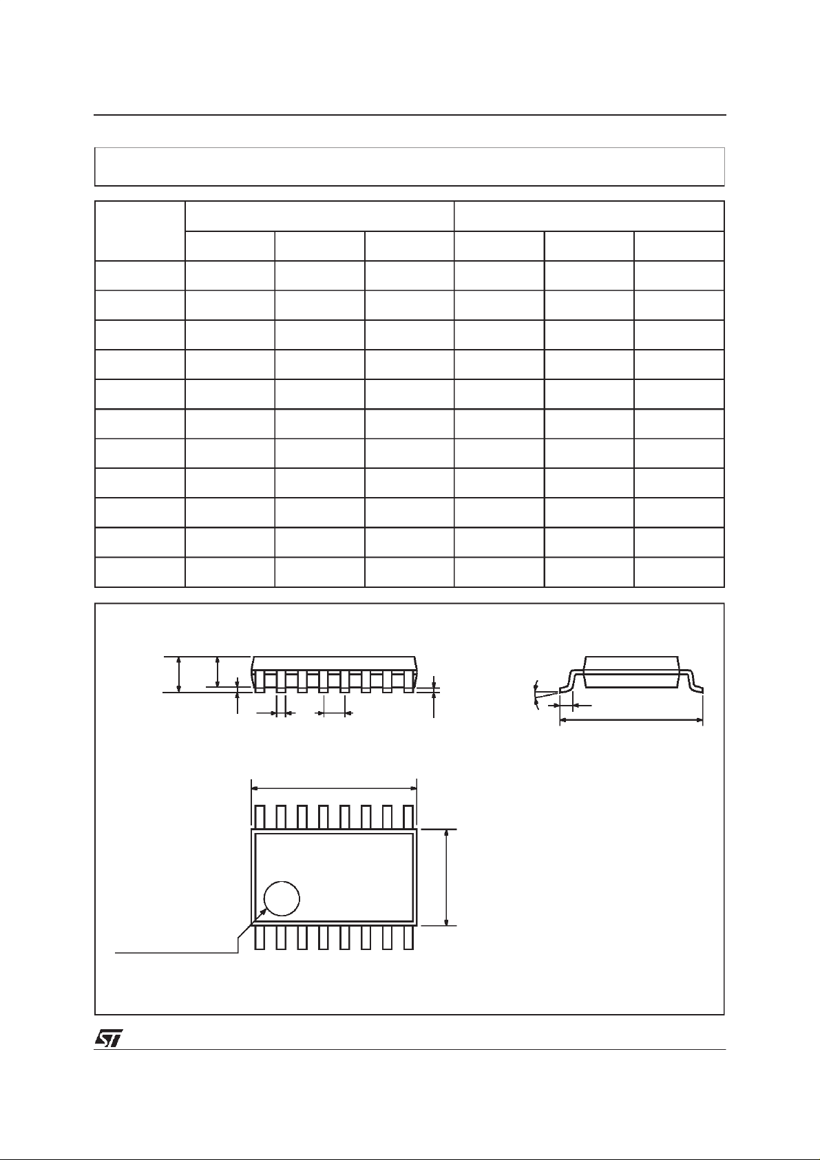
TSSOP16 MECHANICAL DATA
74VHCT138A
DIM.
mm inch
MIN. TYP. MAX. MIN. TYP. MAX.
A 1.1 0.433
A1 0.05 0.10 0.15 0.002 0.004 0.006
A2 0.85 0.9 0.95 0.335 0.354 0.374
b 0.19 0.30 0.0075 0.0118
c 0.09 0.20 0.0035 0.0079
D 4.9 5 5.1 0.193 0.197 0.201
E 6.25 6.4 6.5 0.246 0.252 0.256
E1 4.3 4.4 4.48 0.169 0.173 0.176
e 0.65 BSC 0.0256 BSC
K0
o
o
4
o
8
o
0
o
4
L 0.50 0.60 0.70 0.020 0.024 0.028
o
8
A2
A
A1
PIN 1 IDENTIFICATION
b
e
c
K
L
E
D
E1
1
7/8
Page 8

74VHCT138A
Information furnished isbelieved to be accurate and reliable.However, STMicroelectronics assumes no responsibility forthe consequences
of use of such information nor for any infringement of patents or other rights of third parties which may result from its use. No license is
granted by implicationor otherwise under any patent or patent rights of STMicroelectronics. Specification mentioned in this publication are
subject to change without notice. Thispublication supersedesand replaces all informationpreviously supplied. STMicroelectronics products
are not authorized for use as criticalcomponents in lifesupport devices or systems withoutexpress written approval of STMicroelectronics.
The ST logo isa registered trademark of STMicroelectronics
2000 STMicroelectronics – Printed in Italy – All Rights Reserved
STMicroelectronics GROUP OF COMPANIES
Australia - Brazil - China - Finland - France - Germany - Hong Kong - India - Italy- Japan- Malaysia - Malta - Morocco
Singapore - Spain - Sweden - Switzerland - United Kingdom - U.S.A.
http://www.st.com
.
8/8
 Loading...