

Page 1
QUAD BUS BUFFERS (3-STATE)
■ HIGHSPEED:t
■ LOW POWER DISSIPATION:
I
=4 µA (MAX.) at TA=25oC
CC
■ COMPATIBLEWITHTTL OUTPUTS:
=2V(MIN),VIL=0.8V(MAX)
V
IH
■ POWERDOWNPROTECTIONON INPUTS&
OUTPUTS
■ SYMMETRICALOUTPUTIMPEDANCE:
|I
|=IOL=8 mA(MIN)
OH
■ BALANCEDPROPAGATIONDELAYS:
t
≅ t
PLH
PHL
■ OPERATINGVOLTAGERANGE:
V
(OPR)= 4.5V to 5.5V
CC
■ PINANDFUNCTION COMPATIBLEWITH
74SERIES126
■ IMPROVEDLATCH-UP IMMUNITY
■ LOWNOISE:V
DESCRIPTION
The 74VHCT126A is an advanced high-speed
CMOS QUAD BUS BUFFERS fabricated with
sub-micron silicon gate and double-layer metal
wiringC
2
MOStechnology.
=5ns(TYP.)atVCC=5V
PD
= 0.8V(Max.)
OLP
74VHCT126A
PRELIMINARY DATA
SOP TSSOP
ORDER CODES
PACKAGE TUBE T & R
SOP 74VHCT126AM 74VHCT126AMTR
TSSOP 74VHCT126ATTR
This device requires the 3-STATEcontrol input G
to be set low to place the output into the high
impedancestate.
Power down protection is provided on all inputs
and outputs and 0 to 7V can be accepted on
inputs with no regard to the supply voltage. This
devicecan be usedto interface 5V to 3V.
All inputs and outputs are equipped with
protection circuits against static discharge, giving
them 2KV ESD immunity and transient excess
voltage.
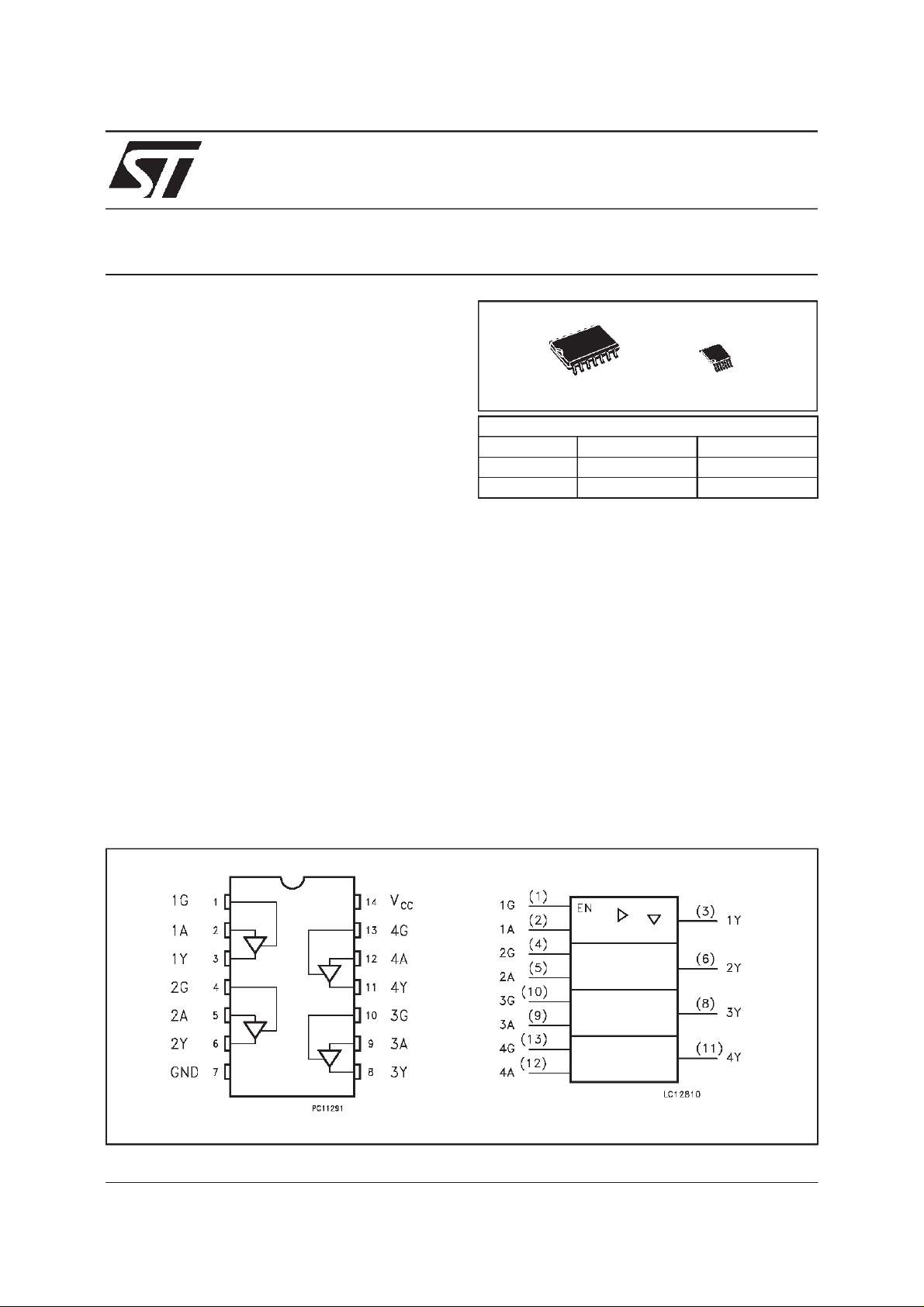
PIN CONNECTION AND IECLOGIC SYMBOLS
March 2000
1/8
Page 2

74VHCT126A
INPUT EQUIVALENTCIRCUIT
PIN DESCRIPTION
PI N No SYMB OL NAME AND FU NCTI O N
1, 4, 10, 13 1G to 4G Output Enable Inputs
2, 5, 9, 12 1A to 4A Data Inputs
3, 6, 8, 11 1Y to 4Y Data Outputs
7 GND Ground (0V)
14 V
CC
Positive Supply Voltage
TRUTH TABLE
AGY
XLZ
LHL
HHH
X:”H” or”L”
Z: High Impedance
ABSOLUTE MAXIMUMRATINGS
Symb o l Para met er Value U n i t
V
V
V
V
I
I
OK
I
or I
I
CC
T
T
AbsoluteMaximumRatingsarethosevaluesbeyondwhichdamage tothedevicemayoccur. Functionaloperationunderthesecondition isnotimplied.
1)Outputin OFFState
2)HighorLowState
Supply Voltage -0.5 to +7.0 V
CC
DC Input Voltage -0.5 to +7.0 V
I
DC Output Voltage (see note 1) -0.5 to +7.0 V
O
DC Output Voltage (see note 2) -0.5 to VCC+ 0.5 V
O
DC Input Diode Current - 20 mA
IK
DC Output Diode Current ± 20 mA
DC Output Current ± 25 mA
O
DC VCCor Ground Current ± 50 mA
GND
Storage Temperature -65 to +150
stg
Lead Temperature (10 sec) 300
L
o
C
o
C
RECOMMENDEDOPERATINGCONDITIONS
Symb o l Para met er Value Unit
V
V
V
V
T
dt/dv
1)Outputin OFFState
2)HighorLowState
from0.8Vto 2V
3)V
IN
2/8
Supply Voltage 4.5 to 5.5 V
CC
Input Voltage 0 to 5.5 V
I
Output Voltage (see note 1) 0 to 5.5 V
O
Output Voltage (see note 2) 0 to V
O
Operating Temperature -40 to +85
op
Input Rise and Fall Time (see note 3) (V
=5.0±0.5V)
CC
CC
0 to 20 ns/V
V
o
C
Page 3

74VHCT126A
DC SPECIFICATIONS
Symb o l Parameter Test C o n di ti o ns Val u e Uni t
T
=25oC -40 to 85oC
A
±0.25 ±2.5 µA
1.35 1.5 mA
µ
µ
V
V
V
V
I
I
∆I
I
OPD
V
CC
High Level Input
IH
(V)
4.5 to 5.5 2 2 V
Min. Typ. Max. Min. Max.
Voltage
Low Level Input
IL
4.5 to 5.5 0.8 0.8 V
Voltage
High Level Output
OH
Voltage
Low Level Output
OL
Voltage
High Impedance
OZ
Output Leakage
4.5 IO=-50µA 4.4 4.5 4.4
4.5 I
=-8 mA 3.94 3.8
O
4.5 IO=50µA 0.0 0.1 0.1
4.5 I
4.5 to 5.5 VI=VIHor V
=8 mA 0.36 0.44
O
IL
VO= 0V to 5.5V
Current
Input Leakage Current 0 to5.5 VI= 5.5V or GND ±0.1 ±1.0 µA
I
I
Quiescent Supply
CC
5.5 VI=VCCorGND 4 40
Current
Additional Worst Case
CC
Supply Current
5.5 One Input at 3.4V,
other input at V
CC
or
GND
Output Leakage
0V
= 5.5V 0.5 5.0
OUT
Current
V
V
A
A
AC ELECTRICAL CHARACTERISTICS (Input tr=tf=3 ns)
Symbol Parameter Test Condition Value Unit
t
Propagation Delay
PLH
t
Time
PHL
Output Enable Time 5.0
t
PZL
t
PZH
t
Output Disable Time 5.0
PLZ
t
PHZ
(*) Voltagerangeis 5.0V ± 0.5V
V
(V)
5.0
5.0
5.0
CC
C
L
(pF)
(*)
15 3.8 5.5 1.0 6.5
(*)
50 5.3 7.5 1.0 8.5
(*)
(*)
(*)
15 RL=1K
50 RL=1KΩ 5.1 7.1 1.0 8.0
50 RL=1K
Min. Typ. Max. Min. Max.
Ω
Ω
=25oC -40 to 85oC
T
A
3.6 5.1 1.0 6.0
6.1 8.8 1.0 10.0 ns
ns
ns
3/8
Page 4

74VHCT126A
CAPACITIVE CHARACTERISTICS
Symbol Parameter Test Conditions Value Unit
=25oC -40 to 85oC
T
A
Min. Typ. Max. Min. Max.
Input Capacitance 4 10 10
C
IN
C
Output Capacitance 10
OUT
Power Dissipation
C
PD
14 pF
Capacitance (note 1)
1)CPDisdefinedasthevalue oftheIC’sinternalequivalentcapacitance whichiscalculatedfromtheoperating currentconsumption without load.(Referto
TestCircuit).Averageopertingcurrent canbe obtainedbythefollowingequation. I
(opr)= CPD• VCC• fIN+ICC/4(percircuit)
CC
DYNAMICSWITCHING CHARACTERISTICS
Symb o l Parameter Test C o n di ti o ns Val u e Uni t
T
V
CC
(V)
V
V
V
Dynamic Low Voltage
OLP
Quiet Output (note 1, 2)
OLV
Dynamic High Voltage
IHD
5.0
5.0 2.0
C
L
=50pF
Min. Typ. Max. Min. Max.
Input (note 1, 3)
V
Dynamic Low Voltage
ILD
5.0 0.8
Input (note 1, 3)
1)Worstcasepackage.
2)Maxnumberofoutputs defined as(n).Datainputsaredriven0Vto5.0V,(n-1)outputsswitching andoneoutputatGND.
3)Maxnumberofdatainputs (n)switching.(n-1)switching0Vto5.0V.Inputs under test switching: 5.0Vtothreshold(V
=25oC -40 to 85oC
A
0.3 0.8
-0.8 -0.3
),0V tothreshold(V
ILD
),f=1MHz.
IHD
pF
pF
V
TESTCIRCUIT
TEST SWITCH
t
PLH,tPHL
t
PZL,tPLZ
t
PZH,tPHZ
CL= 15/50 pF orequivalent (includes jig and probe capacitance)
=1KΩorequivalent
R
L=R1
R
ofpulsegenerator (typically50Ω)
T=ZOUT
Open
V
CC
GND
4/8
Page 5

74VHCT126A
WAVEFORM1: PROPAGATION DELAYS
(f=1MHz;50% dutycycle)
WAVEFORM2: OUTPUTENABLE AND DISABLE TIME(f=1MHz; 50% dutycycle)
5/8
Page 6

74VHCT126A
SO-14 MECHANICALDATA
DIM.
MIN. TYP. MAX. MIN. TYP. MAX.
A 1.75 0.068
a1 0.1 0.2 0.003 0.007
a2 1.65 0.064
b 0.35 0.46 0.013 0.018
b1 0.19 0.25 0.007 0.010
C 0.5 0.019
c1 45 (typ.)
D 8.55 8.75 0.336 0.344
E 5.8 6.2 0.228 0.244
e 1.27 0.050
e3 7.62 0.300
F 3.8 4.0 0.149 0.157
G 4.6 5.3 0.181 0.208
L 0.5 1.27 0.019 0.050
M 0.68 0.026
S 8 (max.)
mm inch
6/8
P013G
Page 7

TSSOP14 MECHANICAL DATA
74VHCT126A
DIM.
mm inch
MIN. TYP. MAX. MIN. TYP. MAX.
A 1.1 0.433
A1 0.05 0.10 0.15 0.002 0.004 0.006
A2 0.85 0.9 0.95 0.335 0.354 0.374
b 0.19 0.30 0.0075 0.0118
c 0.09 0.20 0.0035 0.0079
D 4.9 5 5.1 0.193 0.197 0.201
E 6.25 6.4 6.5 0.246 0.252 0.256
E1 4.3 4.4 4.48 0.169 0.173 0.176
e 0.65 BSC 0.0256 BSC
K0
o
o
4
o
8
o
0
o
4
L 0.50 0.60 0.70 0.020 0.024 0.028
o
8
A2
A
A1
PIN 1 IDENTIFICATION
b
e
c
K
L
E
D
E1
1
7/8
Page 8

74VHCT126A
Information furnished isbelieved to be accurate andreliable. However, STMicroelectronics assumes no responsibility for the consequences
of use of such information nor for any infringement of patents or other rights of third parties which may result from its use. No license is
granted by implication or otherwise under any patent or patent rights of STMicroelectronics. Specification mentioned in this publication are
subject tochange without notice. Thispublication supersedes and replaces allinformation previously supplied. STMicroelectronics products
are not authorized for use as critical components in life support devices or systems withoutexpress written approval of STMicroelectronics.
The ST logo is a registeredtrademark of STMicroelectronics
2000 STMicroelectronics – Printed in Italy – All Rights Reserved
STMicroelectronics GROUP OF COMPANIES
Australia - Brazil - China - Finland - France -Germany - HongKong - India - Italy- Japan- Malaysia - Malta - Morocco
Singapore - Spain- Sweden - Switzerland - United Kingdom - U.S.A.
http://www.st.com
.
8/8
 Loading...