

Page 1
74VHCT02A
QUAD 2-INPUT NOR GATE
■ HIGH SPEED:t
■
LOW POWERDISSIPATION:
I
=2 µA(MAX.) at TA=25oC
CC
■
COMPATIBLEWITH TTL OUTPUTS:
V
=2V(MIN),VIL=0.8V(MAX)
IH
■ POWERDOWN PROTECTIONON INPUTS&
=3.5ns (TYP.)at VCC=5V
PD
OUTPUTS
■ SYMMETRICALOUTPUT IMPEDANCE:
|I
|=IOL=8mA (MIN)
OH
■ BALANCEDPROPAGATIONDELAYS:
t
≅ t
PLH
PHL
■
OPERATINGVOLTAGERAN GE:
V
(OPR)= 4.5Vto5.5V
CC
■ PINANDFUNCTIONCOMPATIBLEWITH
74SERIES02
■ IMPROVEDLATCH-UPIMMUNITY
■
LOWNOISE:V
= 0.8V(Max.)
OLP
DESCRIPTION
The 74VHCT02A is an advanced high-speed
CMOS QUAD 2-INPUT NOR GATE fabricated
with sub-micron silicon gate and double-layer
metalwiring C
2
MOStechnology.
M
(Micro Package)
(TSSOPPackage)
T
ORDERCODES :
74VHCT02AM 74VHCT02AT
The internal circuit is composed of 3 stages
including buffer output, which provide high noise
immunityand stable output.
Power down protection is provided on all inputs
and outputs and 0 to 7V can be accepted on
inputs with no regard to the supply voltage. This
devicecan be usedto interface5V to 3V.
All inputs and outputs are equipped with
protection circuits against static discharge, giving
them 2KV ESD immunity and transient excess
voltage.
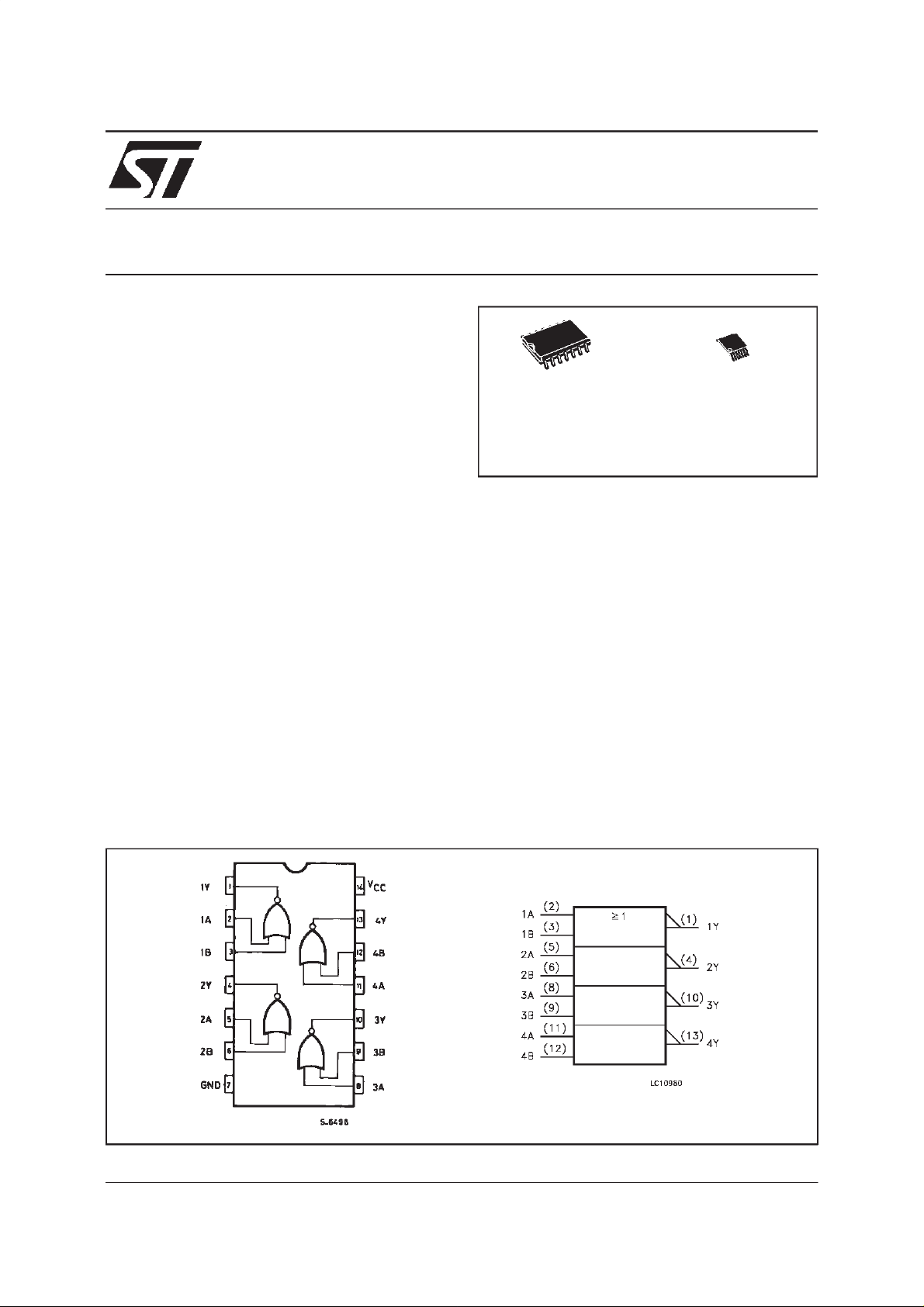
PIN CONNECTION AND IEC LOGIC SYMBOLS
August 1999
1/7
Page 2
74VHCT02A
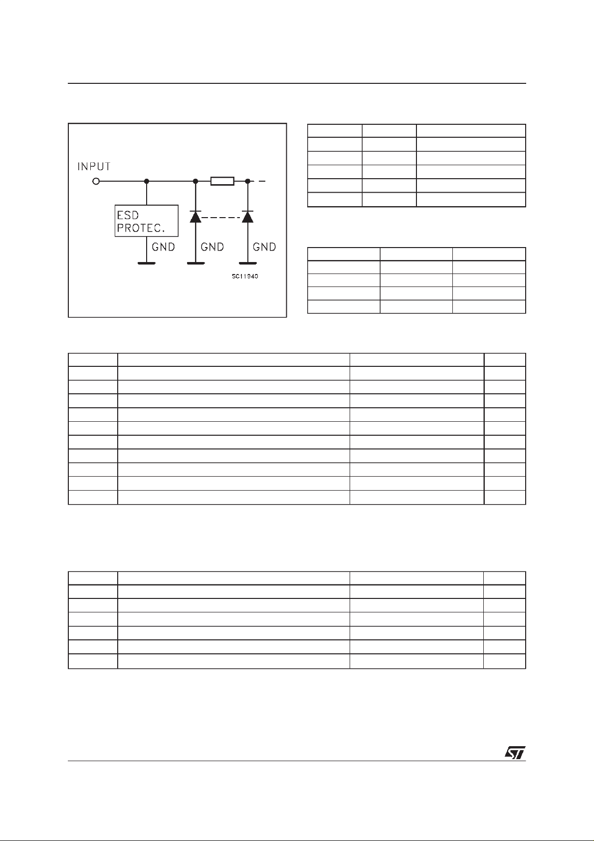
INPUT EQUIVALENTCIRCUIT
PIN DESCRIPTION
PI N No SYMB OL NAME AND F U NCTION
2, 5, 8, 11 1A to 4A Data Inputs
3, 6, 9, 12 1B to 4B Data Inputs
1, 4, 10, 13 1Y to 4Y Data Outputs
7 GND Ground (0V)
14 V
CC
Positive Supply Voltage
TRUTH TABLE
ABY
LLH
LHL
HLL
HHL
ABSOLUTE MAXIMUM RATINGS
Symb o l Para met er Value U n i t
V
V
V
V
I
I
OK
I
or I
I
CC
T
T
AbsoluteMaximum Ratingsarethosevaluesbeyond whichdamagetothedevice mayoccur.Functionaloperationunderthese condition isnotimplied.
=0V
1)V
CC
2)HighorLow State
Supply Voltage -0.5 to +7.0 V
CC
DC Input Voltage -0.5 to +7.0 V
I
DC Output Voltage (see note 1) -0.5 to +7.0 V
O
DC Output Voltage (see note 2) -0.5 to VCC+ 0.5 V
O
DC Input Diode Current - 20 mA
IK
DC Output Diode Current ± 20 mA
DC Output Current ± 25 mA
O
DC VCCor Ground Current ± 50 mA
GND
Storage Temperature -65 to +150
stg
Lead Temperature (10 sec) 300
L
o
C
o
C
RECOMMENDED OPERATING CONDITIONS
Symb o l Para met er Value Unit
V
V
V
V
T
dt/dv
1)VCC=0V
2)HighorLow State
from0.8Vto 2 V
3)V
IN
2/7
Supply Voltage 4.5 to 5.5 V
CC
Input Voltage 0 to 5.5 V
I
Output Voltage (see note 1) 0 to 5.5 V
O
Output Voltage (see note 2) 0 to V
O
Operating Temperature -40 to +85
op
Input Rise and Fall Time (see note 3) (V
=5.0±0.5V)
CC
CC
0 to 20 ns/V
V
o
C
Page 3
74VHCT02A
DC SPECIFICATIONS
Symb o l Para met er Test Conditio ns Val u e Uni t
T
=25oC -40 t o 85oC
A
1.35 1.5 mA
V
V
V
V
I
∆
I
OPD
V
CC
High Level Input
IH
(V)
4.5 to 5.5 2 2 V
Min. Typ. Max. Min. Max.
Voltage
Low Level Input
IL
4.5 to 5.5 0.8 0.8 V
Voltage
High Level Output
OH
Voltage
Low Level Output
OL
Voltage
Input Leakage Current 0 to 5.5 VI= 5.5V or GND ±0.1 ±1.0 µA
I
I
Quiescent Supply
CC
4.5 IO=-50 µ A 4.4 4.5 4.4
4.5 I
=-8 mA 3.94 3.8
O
4.5 IO=50µA 0.0 0.1 0.1
4.5 I
=8 mA 0.36 0.44
O
5.5 VI=VCCorGND 2 20 µA
Current
Additional Worst Case
I
CC
Supply Current
5.5 One Input at 3.4V,
other input at V
CC
or
GND
Output Leakage
0V
= 5.5V 0.5 5.0 µA
OUT
Current
V
V
AC ELECTRICAL CHARACTERISTICS
(Inputt
r=tf
=3 ns)
Symbol Parameter Test Co ndition Value Unit
V
(*)
t
Propagation Delay
PLH
t
Time
PHL
(*)Voltagerangeis5V±0.5V
CC
(V)
C
(pF)
L
Min. Typ. Max. Min. Max.
5.0 15 3.5 5.5 1.0 6.5
5.0
50
=25oC -40 t o 85oC
T
A
4.5 7.5 1.0 8.5
ns
CAPACITIVE CHARACTERISTICS
Symb o l Para met er Test Conditio ns Val u e Uni t
=25oC -40 t o 85oC
T
A
Min. Typ. Max. Min. Max.
Input Capacitance 4 10 10 pF
C
IN
Power Dissipation
C
PD
Capacitance (note 1)
1)CPDisdefinedasthevalueoftheIC’sinternalequivalentcapacitance whichiscalculated fromtheoperating currentconsumption withoutload.(Referto
TestCircuit).Average operating currentcanbeobtainedbythefollowingequation.I
(opr)=CPD• VCC• fIN+ICC/4(perGate)
CC
17 pF
3/7
Page 4

74VHCT02A
DYNAMICSWITCHING CHARACTERISTICS
Symb o l Para met er Test Conditio ns Val u e Uni t
T
V
CC
(V)
V
V
V
Dynamic Low Voltage
OLP
Quiet Output (note 1, 2)
OLV
Dynamic High Voltage
IHD
5.0
5.0 2
C
L
=50pF
Min. Typ. Max. Min. Max.
Input (note 1, 3)
V
Dynamic Low Voltage
ILD
5.0 0.8
Input (note 1, 3)
1)Worstcasepackage.
2)Max numberofoutputsdefinedas (n).Datainputs aredriven0Vto3.0V,(n -1)outputs switchingandoneoutputatGND.
3)Max numberofdatainputs (n)switching.(n-1)switching0Vto3.0V. Inputsundertestswitching: 3.0Vtothreshold(V
TESTCIRCUIT
=25oC -40 t o 85oC
A
0.3 0.8
-0.8 -0.3
),0Vtothreshold(V
ILD
),f=1MHz.
IHD
V
CL= 15/50pF or equivalent (includes jigand probe capacitance)
R
ofpulsegenerator (typically50Ω)
T=ZOUT
WAVEFORM: PROPAGATION DELAYS
4/7
(f=1MHz;50% duty cycle)
Page 5

SO-14 MECHANICAL DATA
74VHCT02A
DIM.
MIN. TYP. MAX. MIN. TYP. MAX.
A 1.75 0.068
a1 0.1 0.2 0.003 0.007
a2 1.65 0.064
b 0.35 0.46 0.013 0.018
b1 0.19 0.25 0.007 0.010
C 0.5 0.019
c1 45 (typ.)
D 8.55 8.75 0.336 0.344
E 5.8 6.2 0.228 0.244
e 1.27 0.050
e3 7.62 0.300
F 3.8 4.0 0.149 0.157
G 4.6 5.3 0.181 0.208
L 0.5 1.27 0.019 0.050
M 0.68 0.026
S 8 (max.)
mm inch
P013G
5/7
Page 6

74VHCT02A
TSSOP14 MECHANICAL DATA
DIM.
mm inch
MIN. TYP. MAX. MIN. TYP. MAX.
A 1.1 0.433
A1 0.05 0.10 0.15 0.002 0.004 0.006
A2 0.85 0.9 0.95 0.335 0.354 0.374
b 0.19 0.30 0.0075 0.0118
c 0.09 0.20 0.0035 0.0079
D 4.9 5 5.1 0.193 0.197 0.201
E 6.25 6.4 6.5 0.246 0.252 0.256
E1 4.3 4.4 4.48 0.169 0.173 0.176
e 0.65 BSC 0.0256 BSC
K0
o
o
4
o
8
o
0
o
4
L 0.50 0.60 0.70 0.020 0.024 0.028
o
8
A
PIN 1 IDENTIFICATION
6/7
A2
A1
b
e
c
K
L
E
D
E1
1
Page 7

74VHCT02A
Information furnished is believed to beaccurate and reliable. However, STMicroelectronics assumes no responsibility for the consequences
of use of such information nor for any infringement of patents or other rights of third parties which may result from its use. No license is
granted by implication or otherwise under anypatent or patent rights of STMicroelectronics. Specification mentioned in thispublication are
subject tochange without notice. This publication supersedes and replaces all information previously supplied. STMicroelectronics products
are notauthorized for use as critical components in life support devices or systems without express written approval of STMicroelectronics.
The ST logo is a trademark of STMicroelectronics
1999 STMicroelectronics – Printed in Italy– All Rights Reserved
STMicroelectronics GROUP OF COMPANIES
Australia - Brazil - Canada - China -France - Germany - Italy - Japan -Korea - Malaysia - Malta -Mexico -Morocco - TheNetherlands -
Singapore -Spain -Sweden - Switzerland- Taiwan -Thailand - UnitedKingdom -U.S.A.
http://www.st.com
.
7/7
 Loading...