

Page 1
1/8June 2001
■ HIGH SPEED: t
PD
= 4.8 ns (TYP.) at VCC = 5V
■ LOW POWER DISSIPATION:
I
CC
= 2 µA (MAX.) at TA=25°C
■ HIGH NOISE IMMUNITY:
V
NIH
= V
NIL
= 28% VCC (MIN.)
■ POWER DOWN PROTECTION ON INPUTS
■ SYMMETRICAL OUTPUT IMPED ANCE:
|I
OH
| = IOL = 8 mA (MIN)
■ BALANCED PROPAGATION DELAYS:
t
PLH
≅ t
PHL
■ OPERATING VOLTAGE RANGE:
V
CC
(OPR) = 2V to 5.5V
■ PIN AND FUNCTION COMPATIBLE WITH
74 SERIES 86
■ IMPROVED LATCH-UP IMMUNITY
■ LOW NOISE: V
OLP
= 0.8V (MAX.)
DESCRIPTION
The 74VHC86 is a n advanced high-speed CM OS
QUAD EXCLUSIVE OR GATE fabricated with
sub-micron silicon gate and double-layer metal
wiring C
2
MOS technology.
Power down protection is provided on all inputs
and 0 to 7V can be accepted on inputs with no
regard to the supply voltage. This device can be
used to interface 5V to 3V.
All inputs and outputs are equipped with
protection circuits against stat ic discharge, giving
them 2KV ESD immunity and transient excess
voltage.
74VHC86
QUAD EXCLUSIVE OR GATE
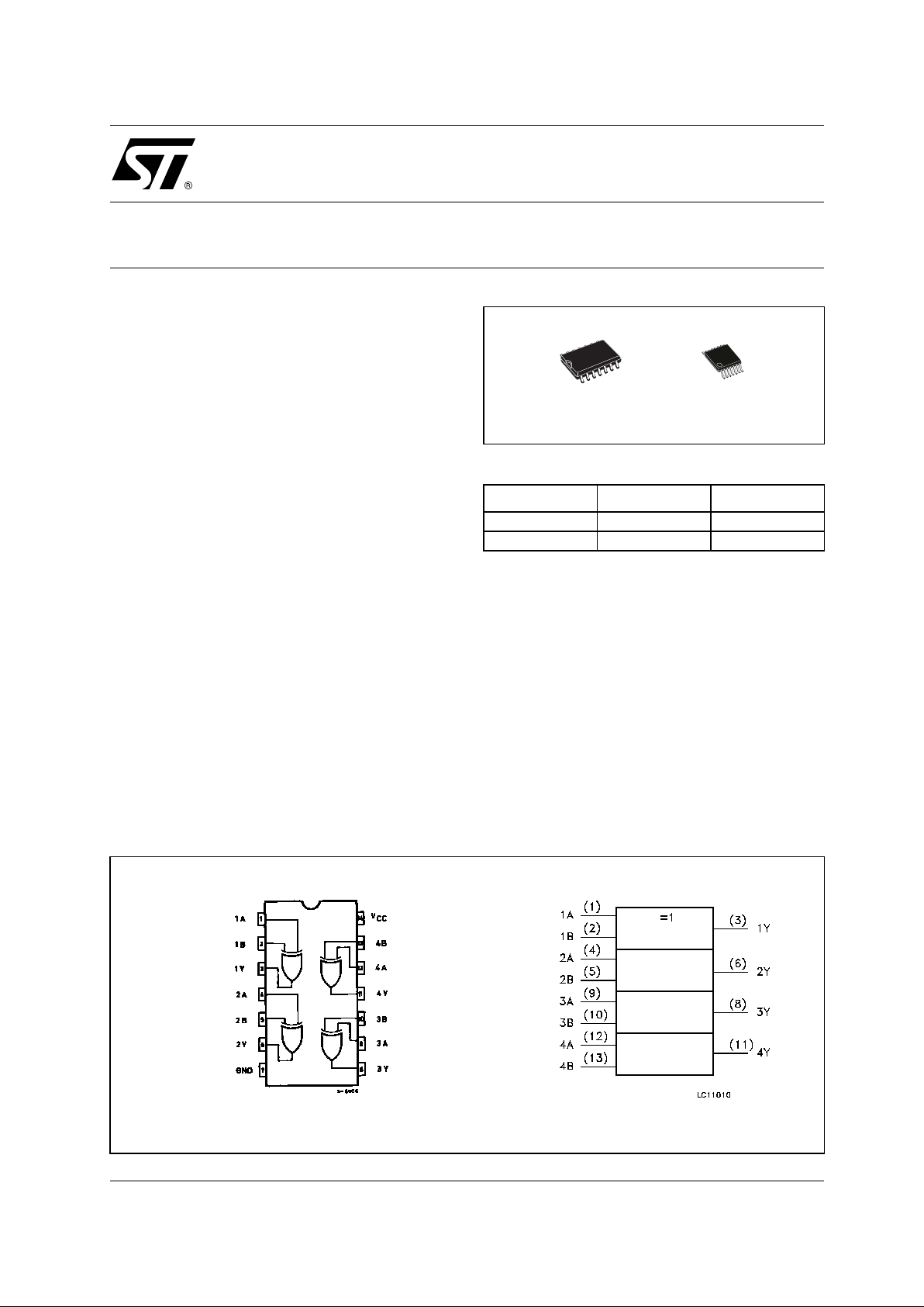
PIN CONNECTION AND IEC LOGIC SYMBOLS
ORDER CODES
PACKAGE TUBE T & R
SOP 74VHC86M 74VHC86MTR
TSSOP 74VHC86TTR
TSSOPSOP
Page 2
74VHC86
2/8
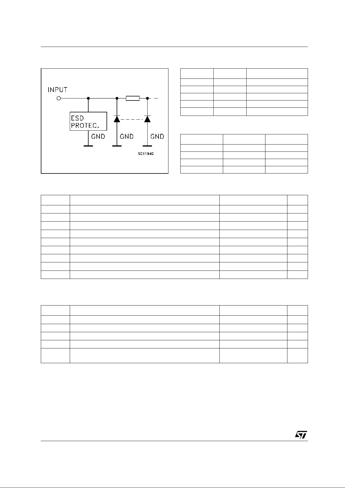
INPUT EQUIVALENT CIRCUIT PIN DESCRIPTION
TRUTH TABLE
ABSOLUTE MAXIMUM RATINGS
Absolute Maximum Ratings are those values beyond which damage to the device may occur. Functional operation under these conditions is
not implied
RECOMMENDED OPERATING CONDITIONS
1) VIN from 30 % to 70% of V
CC
PIN No SYMBOL NAME AND FUNCTION
1, 4, 9, 12 1A to 4A Data Inputs
2, 5, 10, 13 1B to 4B Data Inputs
3, 6, 8, 11 1Y to 4Y Data Outputs
7 GND Ground (0V)
14
V
CC
Positive Supply Voltage
ABY
LLL
LHH
HLH
HHL
Symbol Parameter Value Unit
V
CC
Supply Voltage
-0.5 to +7.0 V
V
I
DC Input Voltage
-0.5 to +7.0 V
V
O
DC Output Voltage -0.5 to VCC + 0.5
V
I
IK
DC Input Diode Current
- 20 mA
I
OK
DC Output Diode Current
± 20 mA
I
O
DC Output Current
± 25 mA
I
CC
or I
GND
DC VCC or Ground Current
± 50 mA
T
stg
Storage Temperature
-65 to +150 °C
T
L
Lead Temperature (10 sec)
300 °C
Symbol Parameter Value Unit
V
CC
Supply Voltage
2 to 5.5 V
V
I
Input Voltage
0 to 5.5 V
V
O
Output Voltage 0 to V
CC
V
T
op
Operating Temperature
-55 to 125 °C
dt/dv
Input Rise and Fall Time (note 1) (V
CC
= 3.3 ± 0.3V)
(V
CC
= 5.0 ± 0.5V)
0 to 100
0 to 20
ns/V
Page 3
74VHC86
3/8
DC SPECIFICATIONS
AC ELECTRICAL CHARACTERISTICS (Input t
r
= tf = 3ns)
(*) Vol tage range is 3. 3V ± 0.3V
(**) Voltage range is 5.0V ±
0.5V
CAPACITIVE CHARACTERISTICS
1) CPD is defined as the value of the IC’s internal equivalent capacitance which is calculated from the operating current consumption without
load. (Refer to Test Circuit). Average operating current can be obtained by the following equation. I
CC(opr)
= CPD x VCC x fIN + ICC/4 (per gate)
Symbol Parameter
Test Condition Value
Unit
V
CC
(V)
T
A
= 25°C
-40 to 85°C -55 to 125°C
Min. Typ. Max. Min. Max. Min. Max.
V
IH
High Level Input
Voltage
2.0 1.5 1.5 1.5
V
3.0 to
5.5
0.7V
CC
0.7V
CC
0.7V
CC
V
IL
Low Level Input
Voltage
2.0 0.5 0.5 0.5
V
3.0 to
5.5
0.3V
CC
0.3V
CC
0.3V
CC
V
OH
High Level Output
Voltage
2.0
I
O
=-50 µA
1.9 2.0 1.9 1.9
V
3.0
I
O
=-50 µA
2.9 3.0 2.9 2.9
4.5
I
O
=-50 µA
4.4 4.5 4.4 4.4
3.0
I
O
=-4 mA
2.58 2.48 2.4
4.5
I
O
=-8 mA
3.94 3.8 3.7
V
OL
Low Level Output
Voltage
2.0
IO=50 µA
0.0 0.1 0.1 0.1
V
3.0
I
O
=50 µA
0.0 0.1 0.1 0.1
4.5
I
O
=50 µA
0.0 0.1 0.1 0.1
3.0
I
O
=4 mA
0.36 0.44 0.55
4.5
I
O
=8 mA
0.36 0.44 0.55
I
I
Input Leakage
Current
0 to
5.5
V
I
= 5.5V or GND
± 0.1 ± 1 ± 1 µA
I
CC
Quiescent Supply
Current
5.5
V
I
= VCC or GND
22020µA
Symbol Parameter
Test Condition Value
Unit
V
CC
(V)
C
L
(pF)
T
A
= 25°C
-40 to 85°C -55 to 125°C
Min. Typ. Max. Min. Max. Min. Max.
t
PLH
t
PHL
Propagation Delay
Time
3.3
(*)
15 7.0 11.0 1.0 13.0 1.0 13.0
ns
3.3
(*)
50 9.5 14.5 1.0 16.5 1.0 16.5
5.0
(**)
15 4.8 6.8 1.0 8.0 1.0 8.0
5.0
(**)
50 6.3 8.8 1.0 10.0 1.0 10.0
Symbol Parameter
Test Condition Value
Unit
T
A
= 25°C
-40 to 85°C -55 to 125°C
Min. Typ. Max. Min. Max. Min. Max.
C
IN
Input Capacitance
6101010pF
C
PD
Power Dissipation
Capacitance
(note 1)
18 pF
Page 4

74VHC86
4/8
DYNAMIC SWITCHING CHARACTERISTICS
1) Worst c ase package .
2) Max number of outp ut s defined as (n). Data inputs are driven 0V to 5.0V, (n-1) outputs switching and one output at GND.
3) Max number of data inputs (n) switching. (n-1) switching 0V to 5.0V. Inputs under test switching: 5.0V to threshold (V
ILD
), 0V to threshold
(V
IHD
), f=1MHz.
TEST CIRCUIT
CL =15/50pF or equivalent (i ncludes jig and probe cap acitance)
R
T
= Z
OUT
of pulse generator (typically 50Ω)
Symbol Parameter
Test Condition Value
Unit
V
CC
(V)
T
A
= 25°C
-40 to 85°C -55 to 125°C
Min. Typ. Max. Min. Max. Min. Max.
V
OLP
Dynamic Low
Voltage Quiet
Output (note 1, 2)
5.0
C
L
= 50 pF
0.3 0.8
V
V
OLV
-0.8 -0.3
V
IHD
Dynamic High
Voltage Input
(note 1, 3)
5.0 3.5 V
V
ILD
Dynamic Low
Voltage Input
(note 1, 3)
5.0 1.5 V
Page 5

74VHC86
5/8
WAVEFORM: PROPAGATION DELAYS (f=1MHz; 50% duty cycle)
Page 6
74VHC86
6/8
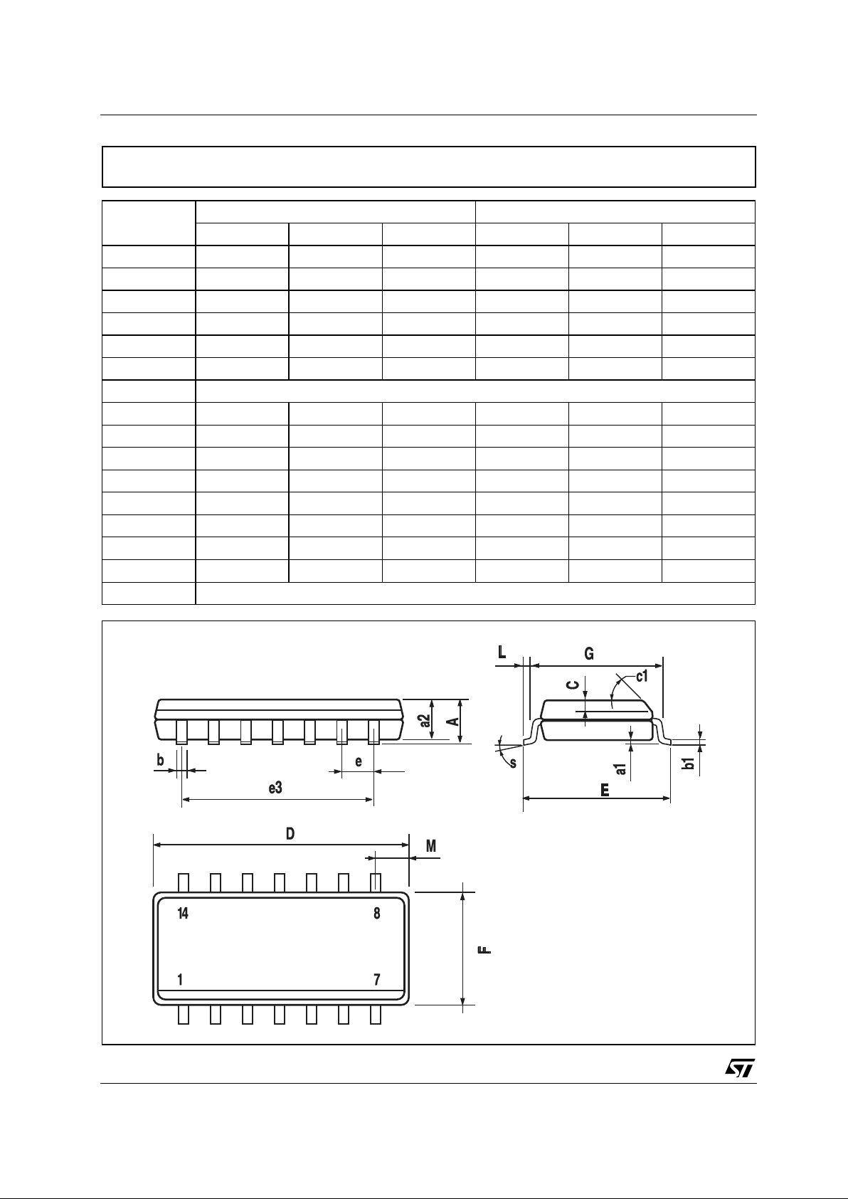
DIM.
mm. inch
MIN. TYP MAX. MIN. TYP. M AX.
A 1.75 0.068
a1 0.1 0.2 0.003 0.007
a2 1.65 0.064
b 0.35 0.46 0.013 0.018
b1 0.19 0.25 0.007 0.010
C 0.5 0.019
c1 45° (typ.)
D 8.55 8.75 0.336 0.344
E 5.8 6.2 0.228 0.244
e 1.27 0.050
e3 7.62 0.300
F 3.8 4.0 0.149 0.157
G 4.6 5.3 0.181 0.208
L 0.5 1.27 0.019 0.050
M 0.68 0.026
S8° (max.)
SO-14 MECHANICAL DATA
PO13G
Page 7

74VHC86
7/8
DIM.
mm. inch
MIN. TYP MAX. MIN. TYP. M AX.
A 1.2 0.047
A1 0.05 0.15 0.002 0.004 0.006
A2 0.8 1 1.05 0.031 0.039 0.041
b 0.19 0.30 0.007 0.012
c 0.09 0.20 0.004 0.0089
D 4.9 5 5.1 0.193 0.197 0.201
E 6.2 6.4 6.6 0.244 0.252 0.260
E1 4.3 4.4 4.48 0.169 0.173 0.176
e 0.65 BSC 0.0256 BSC
K0° 8°0° 8°
L 0.45 0.60 0.75 0.018 0.024 0.030
TSSOP14 MECHANICAL DATA
c
E
b
A2
A
E1
D
1
PIN 1 IDENTIFICATION
A1
L
K
e
0080337D
Page 8

74VHC86
8/8
Information furnished is bel ieved to be accurate and reliable. However, STMicroe lectronics assumes no responsibility for the
consequences of use of such information nor for any infringement of patents or other rights of third parties which may result from
its use. No li cense is granted by implication or otherwise unde r any patent or patent rights of STMicroelectronics. Specifications
mentioned in this publication ar e subject to change without notice. This publication supersedes and replaces all information
previously supplied. S TMicroelectronics products are not authorized for use as critica l components in life suppo rt devices or
systems without express written approval of STMicroelectronics.
© The ST logo is a registered trademark of STMicroelectronics
© 2001 STM icroelectronics - Pr inted in Ital y - All Rights Reserved
STMicr o el ectronics GROUP OF COMPANIES
Australi a - Brazil - Chi na - Finlan d - F rance - Germany - Hong Kong - India - Ital y - Japan - Ma l aysia - Malta - Morocco
Singapo re - Spain - Sweden - Swit zerland - Un i ted Kingdom
© http://www.st.com
 Loading...