

Datasheet 74VHC4053WMX, 74VHC4053WM, 74VHC4053N, 74VHC4053MX, 74VHC4053MTCX Datasheet (Fairchild Semiconductor)
...Page 1
April 1994
Revised April 1999
74VHC4051 • 74VHC4052 • 74VHC4053 8-Channel Analog Multiplexer • Dual 4-Channel Analog Multip lexer • T riple
2-Channel Analog Multiplexer
© 1999 Fairchild Semiconductor Corporation DS011674.prf www.fairchildsemi.com
74VHC4051 • 74VHC4052 • 74VHC4053
8-Channel Analog Multiplexer • Dual 4-Channel Analog
Multiplexer • Triple 2-Channel Analog Multiplexer
General Description
These multiplexers are digitally controlled analog swi tches
implemented in adva nced silicon-gate CMOS tech nology.
These switches have low “on” resistance and low “off” leakages. They are bidirectional switches, thus any analog
input may be used as an output an d vice- ver sa. A lso the se
switches contain linearization circuitry which lowers the
“on” resistance and increases switch linearity. These
devices allow control of up to ±6V (peak) analo g signals
with digital control signals of 0 to 6V. Three supply pins are
provided for V
CC
, ground, and VEE. This enables the con-
nection of 0–5V logic signals when V
CC
= 5V and an analog
input range of ±5V when V
EE
= 5V. All three devices also
have an inhibit control which when high will disable all
switches to their off state. All a nalog inputs and outputs
and digital inputs are pro tected from ele ctrostatic damage
by diodes to V
CC
and ground.
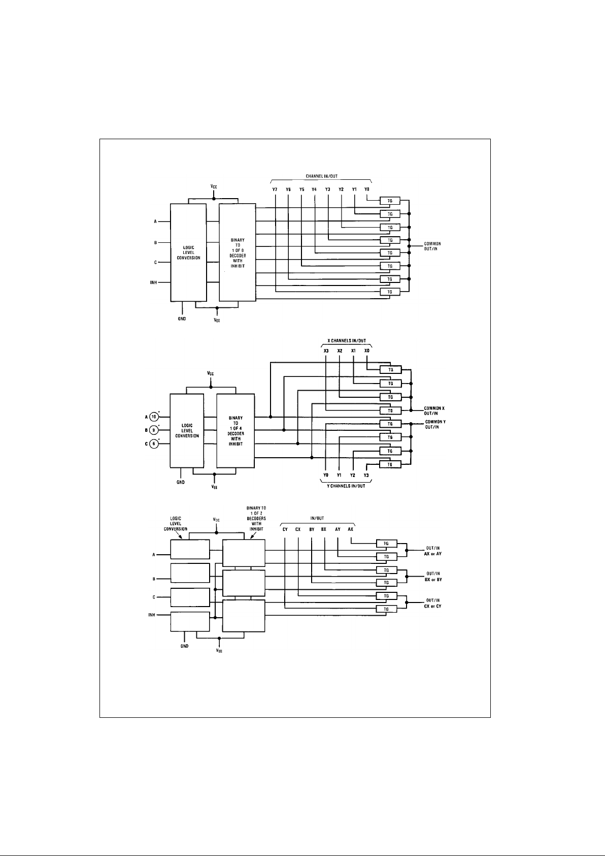
VHC4051: This device co nnects together the outputs of 8
switches, thus achieving an 8 channel Multiplexer. The
binary code placed on the A, B , and C select lines dete rmines which one o f the eight switches is “on”, and connects one of the eight inputs to the common output.
VHC4052: This device co nnects together the outputs of 4
switches in two sets, thu s achieving a pair of 4-channel
multiplexers. The binary code placed on the A, and B
select lines determine which switch in each 4 channel section is “on”, connecting one of the fo ur inputs in each section to its common output. This enables the implementation
of a 4-channel differential multiplexer.
VHC4053: This device conta ins 6 switches whos e outputs
are connected together in pair s, thus impl ementing a tripl e
2 channel multiplexer, or the equivalent of 3 single-poledouble throw configur ations. Each of the A, B, o r C select
lines independently co ntr ols on e pair of switches, selecting
one of the two switches to be “on”.
Features
■ Wide analog input voltage range: ±6V
■ Low “on” resistance: 50 typ. (V
CC–VEE
= 4.5V)
30 typ. (V
CC–VEE
= 9V)
■ Logic level translat ion to enable 5V logic w ith ±5V ana-
log signals
■ Low quiescent current: 80 µA maximum
■ Matched switch characteristic
■ Pin and function compatible with the 74HC4051/ 4052/
4053
Ordering Code:
Surface mount pack ages are also available on Tape and Reel. Specify by appending the s uffix let te r “X” to the ordering code .
Order Number Package Number Package Description
74VHC4051M M16A 16-Lead Small Outline Integrated Circuit (SOIC), JEDEC MS-012, 0.150” Narrow
74VHC4051WM M16B 16-Lead Small Outline Integrated Circuit (SOIC), JEDEC MS-013, 0.300” Wide
74VHC4051MTC MTC16 16-Lead Thin Shrink Small Outline Package (TSSOP), JEDEC MO-153, 4.4mm Wide
74VHC4051N N16E 16-Lead Plastic Dual-In-Line Package (PDIP), JEDEC MS-001, 0.300” Wide
74VHC4052M M16A 16-Lead Small Outline Integrated Circuit (SOIC), JEDEC MS-012, 0.150” Narrow
74VHC4052WM M16B 16-Lead Small Outline Integrated Circuit (SOIC), JEDEC MS-013, 0.300” Wide
74VHC4052MTC MTC16 16-Lead Thin Shrink Small Outline Package (TSSOP), JEDEC MO-153, 4.4mm Wide
74VHC4052N N16E 16-Lead Plastic Dual-In-Line Package (PDIP), JEDEC MS-001, 0.300” Wide
74VHC4053M M16A 16-Lead Small Outline Integrated Circuit (SOIC), JEDEC MS-012, 0.150” Narrow
74VHC4053WM M16B 16-Lead Small Outline Integrated Circuit (SOIC), JEDEC MS-013, 0.300” Wide
74VHC4053MTC MTC16 16-Lead Thin Shrink Small Outline Package (TSSOP), JEDEC MO-153, 4.4mm Wide
74VHC4053N N16E 16-Lead Plastic Dual-In-Line Package (PDIP), JEDEC MS-001, 0.300” Wide
Page 2
www.fairchildsemi.com 2
74VHC4051 • 74VHC4052 • 74VHC4053
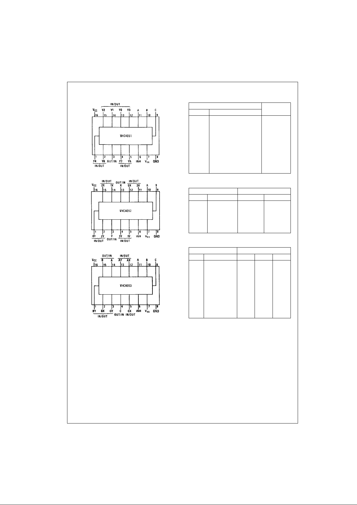
Connection Diagrams
Top View
Top View
Top View
Tr uth Tables
4051
4052
4053
Input “ON”
INHCBAChannel
H XXX None
L LLL Y0
LLLH Y1
LLHL Y2
LLHH Y3
LHLL Y4
LHLH Y5
LHHL Y6
L HHH Y7
Inputs “ON” Channels
INH B A X Y
HXXNone None
LLL 0X 0Y
LLH 1X 1Y
LHL 2X 2Y
LHH 3X 3Y
Input “ON” Channels
INHCBA C B A
H X X X None None None
L L L L CX BX AX
LLLHCX BX AY
L L H L CX BY AX
LLHHCX BY AY
L H L L CY BX AX
LHLHCY BX AY
L H H L CY BY AX
L HHH CY BY AY
Page 3
3 www.fairchildsemi.com
74VHC4051 • 74VHC4052 • 74VHC4053
Logic Diagrams
74VHC4051
74VHC4052
74VHC4053
Page 4

www.fairchildsemi.com 4
74VHC4051 • 74VHC4052 • 74VHC4053
Absolute Maximum Ratings(Note 1)
(Note 2)
Recommended Operating
Conditions
Note 1: Absolute Maximum Ratings are those values beyond which dam-
age to the device may occur.
Note 2: Unless otherwise specified all voltages are referen c ed to ground.
Note 3: Power Dissipation temper ature dera ting — plas tic “N” packa ge: −
12 mW/°C from 65 °C to 85°C.
Supply Voltage (VCC) −0.5 to +7.5V
Supply Voltage (V
EE
) +0.5 to −7.5V
Control Input Voltage (V
IN
) −1.5 to VCC+1.5V
Switch I/O Voltage (V
IO
)V
EE
−0.5 to VCC+0.5V
Clamp Diode Current (I
IK
, IOK) ±20 mA
Output Current, per pin (I
OUT
) ±25 mA
V
CC
or GND Current, per pin (ICC) ±50 mA
Storage Temperature Range
(T
STG
) −65°C to +150°C
Power Dissipation (P
D
)
(Note 3) 600 mW
S.O. Package only 500 mW
Lead Temperature (T
L
)
(Soldering 10 seconds) 260°C
Min Max Units
Supply Voltage (V
CC
)26V
Supply Voltage (V
EE
)0−6V
DC Input or Output Voltage 0 V
CC
V
(V
IN
, V
OUT
)
Operating Temperature Range
(T
A
) −40 +85 °C
Input Rise or Fall Times
(t
r
, tf)
V
CC
= 2.0V 1000 ns
V
CC
= 4.5V 500 ns
V
CC
= 6.0V 400 ns
Page 5

5 www.fairchildsemi.com
74VHC4051 • 74VHC4052 • 74VHC4053
DC Electrical Characteristics (Note 4)
Note 4: For a pow er s upply of 5V ±10% the worst case on resistances (RON) occurs for VHC a t 4. 5V. Thus the 4.5V values should be used when designing
with this supply. Worst case V
IH
and VIL occur at V
CC
= 5.5V and 4. 5V respectively. (The VIH value at 5.5V is 3.85V.) The worst c as e leakage current occur
for CMOS at the higher v oltage and so the 5.5V values should be used.
Note 5: At supply voltages (V
CC–VEE
) approaching 2V the anal og switc h on resist ance beco mes ext remely non -linear. Therefore it is reco mmended t hat
these devices be use d t o tr ansmit digital only when us ing these supply voltages.
Note 6: Adjust 0 dB for f = 1 kHz (Null R1/R
ON
Attenuation).
Symbol Parameter Conditions
V
EE
V
CC
TA = 25°CTA = −40 to 85°C
Units
Typ Guaranteed Limits
V
IH
Minimum HIGH Level 2.0V 1.5 1.5 V
Input Voltage 4.5V 3.15 3.15 V
6.0V 4.2 4.2 V
V
IL
Maximum LOW Level 2.0V 0.5 0.5 V
Input Voltage 4.5V 1.35 1.35 V
6.0V 1.8 1.8 V
R
ON
Maximum “ON” Resistance V
INH
= VIL, IS = 2.0 mA GND 4.5V 40 160 200 Ω
(Note 5) V
IS
= VCC to V
EE
−4.5V 4.5V 30 120 150 Ω
(Figure 1) −6.0V 6.0V 20 100 125 Ω
V
INH
= VIL, IS = 2.0 mA GND 2.0V 100 230 280 Ω
V
IS
= VCC or V
EE
GND 4.5V 40 110 140 Ω
(Figure 1) −4.5V 4.5V 20 90 120 Ω
−6.0V 6.0V 15 80 100 Ω
R
ON
Maximum “ON” Resistance V
INH
= V
IL
GND 4.5V 10 20 25 Ω
Matching V
IS
= VCC to GND −4.5V 4.5V 5 10 15 Ω
−6.0V 6.0V 5 10 12 Ω
I
N
Maximum Control V
IN
= VCC or GND ±.05 ±0.5 µA
Input Current V
CC
= 2 − 6V
I
CC
Maximum Quiescent V
IN
= VCC or GND GND 6.0V 4 40 µA
Supply Current I
OUT
= 0 µA −6.0V 6.0V 8 80 µA
I
IZ
Maximum Switch “OFF” V
OS
= VCC or V
EE
GND 6.0V ±60 ±300 nA
Leakage Current V
IS
= VEE or V
CC
−6.0V 6.0V ±100 ±500 nA
(Switch Input) V
INH
= VIH (Figure 2)
I
IZ
Maximum Switch “ON” V
IS
= VCC to V
EE
GND 6.0V ±0.1 ±1.0 µA
Leakage Current VHC4051 V
INH
= V
IL
−6.0V 6.0V ±0.2 ±2.0 µA
(Figure 3)
V
IS
= VCC to V
EE
GND 6.0V ±0.050 ±0.5 µA
VHC4052 V
INH
= V
IL
−6.0V 6.0V ±0.1 ±1.0 µA
(Figure 3)
V
IS
= VCC to V
EE
GND 6.0V ±0.05 ±0.5 µA
VHC4053 V
INH
= V
IL
−6.0V 6.0V ±0.5 ±0.5 µA
(Figure 3)
I
IZ
Maximum Switch V
OS
= VCC or V
EE
GND 6.0V ±0.1 ±1.0 µA
“OFF” Leakage VHC4051 V
IS
= VEE or V
CC
−6.0V 6.0V ±0.2 ±2.0 µA
Current (Common Pin) V
INH
= V
IH
V
OS
= VCC or V
EE
GND 6.0V ±0.05 ±0.5 µA
VHC4052 V
IS
= VEE or V
CC
−6.0V 6.0V ±0.1 ±1.0 µA
V
INH
= V
IH
V
OS
= VCC or V
EE
GND 6.0V ±0.05 ±0.5 µA
VHC4053 V
IS
= VEE or V
CC
−6.0V 6.0V ±0.05 ±0.5 µA
V
INH
= V
IH
Page 6

www.fairchildsemi.com 6
74VHC4051 • 74VHC4052 • 74VHC4053
AC Electrical Characteristics
V
CC
= 2.0V − 6.0V, V
EE
= 0V − 6V, C
L
= 50 pF (unless otherwise specified)
Symbol Parameter Conditions
VEEV
CC
TA=25°CTA=−40 to 85°C
Units
Typ Guaranteed Limits
t
PHL
, t
PLH
Maximum Propagation Delay
Switch In to Out
GND 3.3V 25 35 40 ns
GND 4.5V 5 12 15 ns
−4.5V 4.5V 4 8 12 ns
−6.0V 6.0V 3 7 11 ns
t
PZL
, t
PZH
Maximum Switch Turn “ON”
Delay
RL = 1 kΩ GND 3.3V 92 200 250 ns
GND 4.5V 69 87 ns
−4.5V 4.5V 16 46 58 ns
−6.0V 6.0V 15 41 51 ns
t
PHZ
, t
PLZ
Maximum Switch Turn “OFF”
Delay
GND 3.3V 65 170 210 ns
GND 4.5V 28 58 73 ns
−4.5V 4.5V 18 37 46 ns
−6.0V 6.0V 16 32 41 ns
f
MAX
Minimum Switch GND 4.5V 30 MHz
Frequency Response −4.5V 4.5V 35 MHz
20 log (VI/VO) = 3 dB
Control to Switch RL = 600Ω,VIS = 4 V
PP
0V 4.5V 1080 mV
Feedthrough Noise f = 1 MHz, VIS = 8 V
PP
−4.5V 4.5V 250 mV
CL = 50 pF
Crosstalk between RL = 600Ω,V
IS
= 4 V
PP
0V 4.5 −52 dB
any Two Switches f = 1 MHz V
IS
= 8 V
PP
−4.5V 4.5V −50 dB
Switch OFF Signal RL = 600Ω,V
IS
= 4 V
PP
0V 4.5V −42 dB
Feedthrough f = 1 MHz, V
IS
= 8 V
PP
−4.5V 4.5V −44 dB
Isolation V
CTL
= V
IL
THD Sinewave Harmonic RL = 10 kΩ,V
IS
= 4 V
PP
0V 4.5V 0.013 %
Distortion CL = 50 pF, V
IS
= 8 V
PP
−4.5V 4.5V 0.008 %
f = 1 kHz
C
IN
Maximum Control 5 10 10 pF
Input Capacitance
C
IN
Maximum Switch Input 15 pF
Input Capacitance 4051 Common 90
4052 Common 45
4053 Common 30
C
IN
Maximum Feedthrough 5 pF
Capacitance
Page 7

7 www.fairchildsemi.com
74VHC4051 • 74VHC4052 • 74VHC4053
AC Test Circuits and Switching Time W aveforms
FIGURE 1. “ON” Resistance
FIGURE 2. “OFF” Channel Leakage Current
FIGURE 3. “ON” Channel Leakage Current
FIGURE 4. t
PHL
, t
PLH
Propagation Delay Time Signal Input to Signal Output
FIGURE 5. t
PZL
, t
PLZ
Propagation Delay Time Control to Signal Output
FIGURE 6. t
PZH
, t
PHZ
Propagation Delay TIme Control to Signal Output
FIGURE 7. Crosstalk: Control Input to Signal Output
Page 8

www.fairchildsemi.com 8
74VHC4051 • 74VHC4052 • 74VHC4053
AC Test Circuits and Switching Time Wavef orms (Continued)
FIGURE 8. Crosstalk Between Any Two Switches
Typical Performance Characteristics
Typical “On” Resi stance
vs Input Voltage
VCC=−V
EE
Special Considerations
In certain appli catio ns the external load-resi stor cu rr ent ma y in cl ude b oth VCC and signal line com pon en ts. To avoid drawing V
CC
current when switch cur ren t fl o ws into the analog switch pins, the volt a ge d ro p ac ross the sw itch mus t no t exce ed
1.2V (calculated from the ON resistance).
Page 9

9 www.fairchildsemi.com
74VHC4051 • 74VHC4052 • 74VHC4053
Physical Dimensions inches (millimeters) unless otherwise noted
16-Lead Small Outline Integrated Circuit (SOIC), JEDEC MS-012, 0.150” Narrow
Package Number M16A
16-Lead Small Outline Intergrated Circuit (SOIC), JEDEC MS-013, 0.300” Wide
Package Number M16B
Page 10

www.fairchildsemi.com 10
74VHC4051 • 74VHC4052 • 74VHC4053
Physical Dimensions inches (millimeters) unless otherwise noted (Continued)
16-Lead Thin Shrink Small Outline Package (TSSOP), JEDEC MO-153, 4.4mm Wide
Package Number MTC16
Page 11

Fairchild does not assume any responsibility for use of any circuitry described, no circuit patent licenses are implied and Fairchild reserves the right at any time without notice to change said circuitry and specifications.
74VHC4051 • 74VHC4052 • 74VHC4053 8-Channel Analog Multiplexer • Dual 4-Channel Analog Multiplexer • T riple
2-Channel Analog Multiplexer
LIFE SUPPORT POLICY
FAIRCHILD’S PRODUCTS ARE NOT AUTHORIZED FOR USE AS CRITICAL COMPONENTS IN LIFE SUPPORT
DEVICES OR SYSTEMS WITHOUT THE EXPRESS WRITTEN APPROVAL OF THE PRESIDENT OF FAIRCHILD
SEMICONDUCTOR CORPORATION. As used herein:
1. Life support devices or systems are dev ices or syste ms
which, (a) are intended for surgical implant into the
body, or (b) support or sustain life, and (c) whose failure
to perform when properly used in accordance with
instructions for use provided i n the labe li ng, can be re asonably expected to result in a significant injury to the
user.
2. A critical componen t in any compo nent o f a li fe supp ort
device or system whose failu re to perform can b e reasonably expected to c ause th e fa i lure of the li fe s upp or t
device or system, or to affect its safety or effectiveness.
www.fairchildsemi.com
Physical Dimensions inches (millimeters) unless otherwise noted (Continued)
16-Lead Plastic Dual-In-Line Package (PDIP), JEDEC MS-001, 0.300” Wide
Package Number N16E
 Loading...