

Page 1
74VHC257
QUAD 2 CHANNEL MULTIPLEXER (3-STATE)
June 1999
■ HIGHSPEED :t
PD
=3.7ns (TYP.)atVCC=5V
■ LOWPOWERDISSIPATION:
I
CC
=4µA (MAX.)at TA=25oC
■ HIGHNOISEIMMUNITY:
V
NIH=VNIL
=28%VCC(MIN.)
■ POWERDOWNPROTECTIONON INPUTS
■ SYMMETRICALOUTPUTIMPEDANCE:
|I
OH
|=IOL=8 mA(MIN)
■ BALANCEDPROPAGATIONDELAYS:
t
PLH≅tPHL
■ OPERATINGVOLTAGERANGE:
V
CC
(OPR)=2V to5.5V
■ PINAND FUNCTIONCOMPATIBLEWITH
74SERIES257
■ IMPROVEDLATCH-UP IMMUNITY
■ LOWNOISEV
OLP
=0.8V(Max.)
DESCRIPTION
The 74VHC257 is an advanced high-speed
CMOS QUAD 2 CHANNEL MULTIPLEXER
(3-STATE)fabricated withsub-micron silicon gate
and double-layer metal wiring C
2
MOS
technology.
It is composed of four independent 2 channel
multiplexers with common SELECT and ENABLE
INPUT.
The 74VHC257is a non inverting multiplexer.
When the ENABLE INPUT is held ”High”, all
outputs become high impedance state. If
SELECT INPUT is held ”Low”, ”A” data is
selected, when SELECT INPUT is ”High”, ”B”
datais chosen.
Power down protection is provided on all inputs
and 0 to 7V can be accepted on inputs with no
regard to the supply voltage. This device can be
used to interface5V to 3V.
All inputs and outputs are equipped with
protection circuits against static discharge, giving
them 2KV ESD immunity and transient excess
voltage.
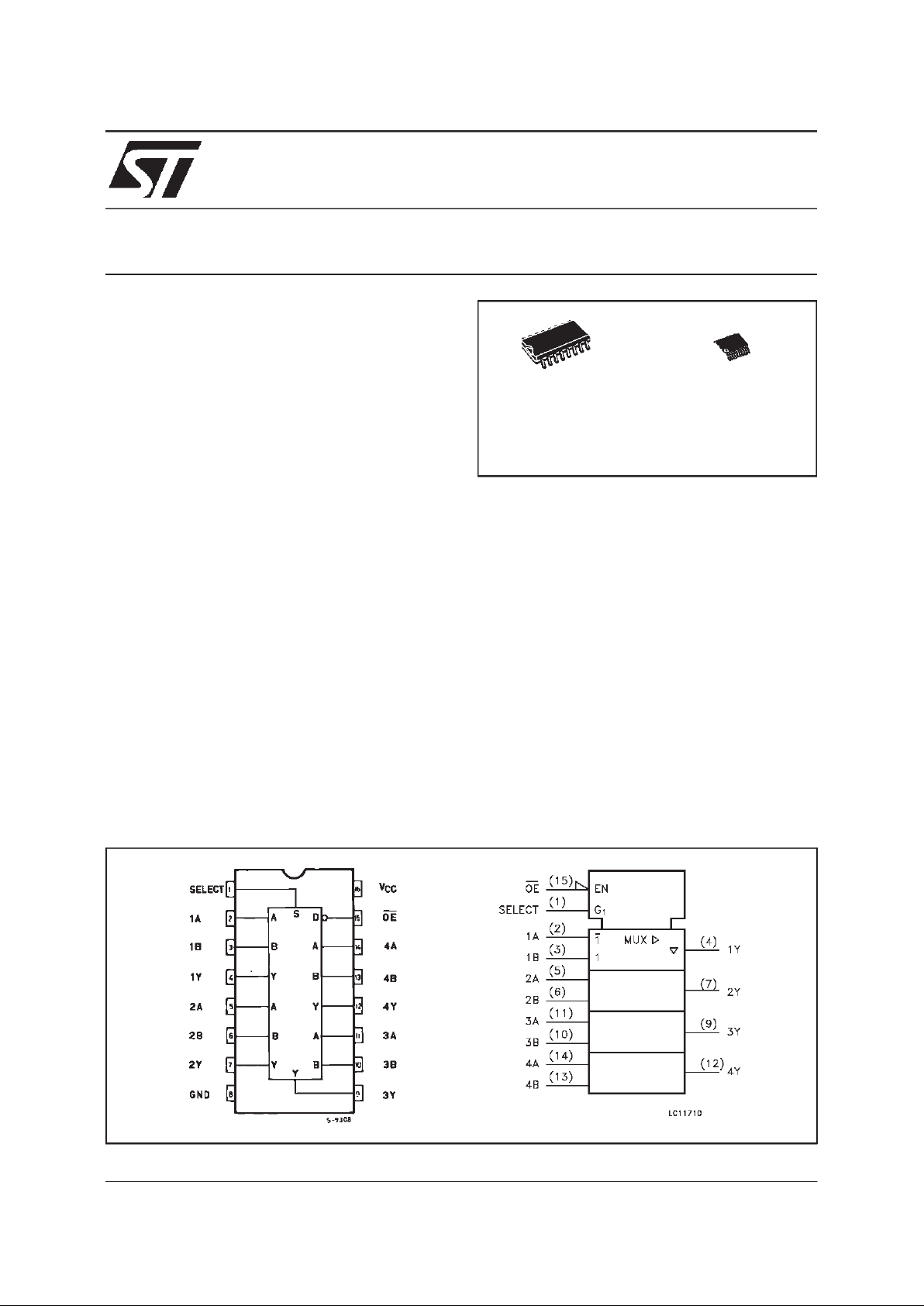
PIN CONNECTION ANDIEC LOGIC SYMBOLS
M
(Micro Package)
T
(TSSOPPackage)
ORDERCODES :
74VHC257M 74VHC257T
1/9
Page 2
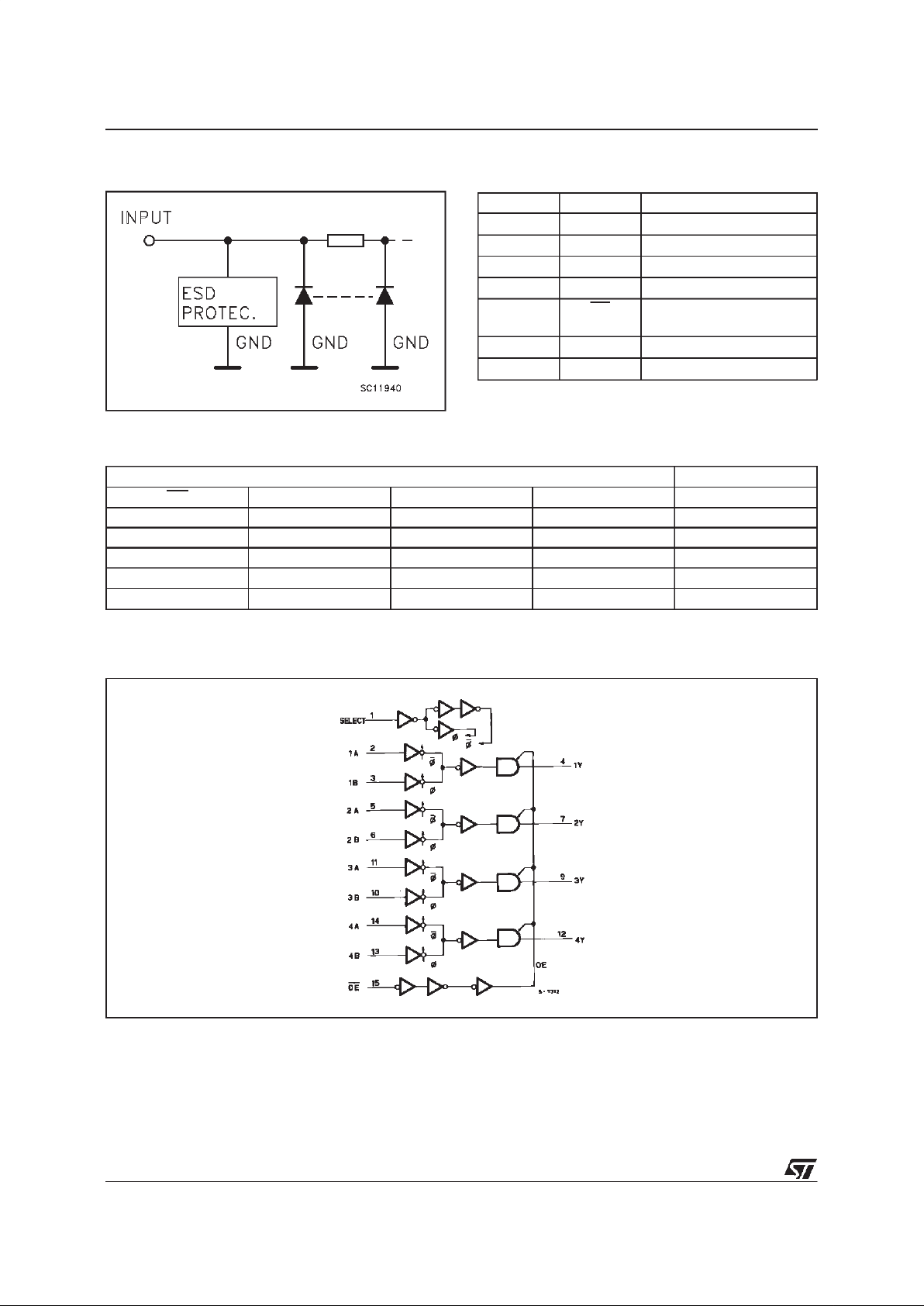
INPUT EQUIVALENTCIRCUIT
LOGICDIAGRAM
PIN DESCRIPTION
PI N No SYM BO L NAM E AND FUNCT I O N
1 SELECT Common Data Select Input
2, 5, 14, 11 1A to 4A Data Input From Source A
3, 6, 13, 10 1B to 4B Data Inputs from Source B
4, 7, 12, 9 1Y to 4Y 3 State Multiplexer Outputs
15 OE 3 State Output Enable
Inputs (Active LOW)
8 GND Ground (0V)
16 V
CC
Positive Supply Voltage
TRUTH TABLE
INPUTS OUTPUTS
OE SELECT A B Y
HXXXZ
LLLXL
LLHXH
LHXLL
LHXHH
X= DON’T CARE Z = HIGHIMPEDANCE
Thislogic diagram has notbe used to estimate propagation delays
74VHC257
2/9
Page 3
ABSOLUTE MAXIMUM RATINGS
Symb o l Para met er Val u e Uni t
V
CC
Supply Voltage -0.5 to +7.0 V
V
I
DC Input Voltage -0.5 to +7.0 V
V
O
DC Output Voltage -0.5 to VCC+ 0.5 V
I
IK
DC Input Diode Current - 20 mA
I
OK
DC Output Diode Current ± 20 mA
I
O
DC Output Current
±
25 mA
I
CC
or I
GND
DC VCCor Ground Current
±
50 mA
T
stg
Storage Temperature -65 to +150
o
C
T
L
Lead Temperature (10 sec) 300
o
C
AbsoluteMaximum Ratingsarethosevaluesbeyondwhichdamageto thedevicemayoccur. Functionaloperationundertheseconditionisnotimplied.
RECOMMENDED OPERATING CONDITIONS
Symb o l Para met er Value Un it
V
CC
Supply Voltage 2.0 to 5.5 V
V
I
Input Voltage 0 to 5.5 V
V
O
Output Voltage 0 to V
CC
V
T
op
Operating Temperature -40 to +85
o
C
dt/dv
Input Rise and Fall Time (see note 1) (V
CC
=3.3±0.3V)
(V
CC
=5.0±0.5V)
0 to 100
0to20
ns/V
ns/V
1)VINfrom30%to70%of V
CC
DC SPECIFICATIONS
Symb o l Para met er Test Co n dit i ons Val u e Uni t
V
CC
(V)
T
A
=25oC -40 to 85oC
Min. Typ. Max. Min. Max.
V
IH
High Level Input
Voltage
2.0 1.5 1.5
V
3.0 to 5.5 0.7V
CC
0.7V
CC
V
IL
Low Level Input
Voltage
2.0 0.5 0.5
V
3.0 to 5.5 0.3V
CC
0.3V
CC
V
OH
High Level Output
Voltage
2.0 IO=-50µA 1.9 2.0 1.9
V
3.0 I
O
=-50µA 2.9 3.0 2.9
4.5 I
O
=-50 µA 4.4 4.5 4.4
3.0 I
O
=-4 mA 2.58 2.48
4.5 I
O
=-8 mA 3.94 3.8
V
OL
Low Level Output
Voltage
2.0 IO=50 µ A 0.0 0.1 0.1
V
3.0 I
O
=50µA 0.0 0.1 0.1
4.5 I
O
=50 µA 0.0 0.1 0.1
3.0 I
O
=4 mA 0.36 0.44
4.5 I
O
=8 mA 0.36 0.44
I
OZ
High Impedance
Output Leakage
Current
5.5
VI=VIHor V
IL
VO=VCCor GND
±0.25 ±2.5 µA
I
I
Input Leakage Current 0 to5.5 VI= 5.5V or GND
±
0.1
±
1.0
µ
A
I
CC
Quiescent Supply
Current
5.5 VI=VCCorGND 4 40
µ
A
74VHC257
3/9
Page 4

CAPACITIVE CHARACTERISTICS
Symb o l Para met er Test Co n dit i ons Val u e Uni t
T
A
=25oC -40 to 85oC
Min. Typ. Max. Min. Max.
C
IN
Input Capacitance 4 10 10
pF
C
OUT
Output Capacitance 6
pF
C
PD
Power Dissipation
Capacitance (note 1)
23 pF
1)CPDisdefinedas thevalue oftheIC’sinternalequivalentcapacitance whichiscalculated fromtheoperatingcurrent consumptionwithoutload.(Referto
TestCircuit).Averageoperatingcurrent canbe obtainedbythefollowingequation.I
CC
(opr)=CPD• VCC• fIN+ICC/4 (per Channel)
AC ELECTRICAL CHARACTERISTICS
(Inputt
r=tf
=3 ns)
Symbol Parameter Test Conditi on Value Unit
V
CC
(V)
C
L
(pF)
T
A
=25oC -40 to 85oC
Min. Typ. Max. Min. Max.
t
PLH
t
PHL
Propagation Delay
Time
A, B to Y
3.3
(*)
15 5.8 9.3 1.0 11.0
ns
3.3
(*)
50 8.3 12.8 1.0 14.5
5.0
(**)
15 3.6 5.9 1.0 7.0
5.0
(**)
50 5.1 7.9 1.0 9.0
t
PLH
t
PHL
Propagation Delay
Time
SELECT to Y
3.3
(*)
15 7.0 11.0 1.0 13.0
ns
3.3
(*)
50 9.5 14.5 1.0 16.5
5.0
(**)
15 4.0 6.8 1.0 8.0
5.0
(**)
50 5.5 8.8 1.0 10.0
t
PZL
t
PZH
Output Enable Time 3.3
(*)
15 6.7 10.5 1.0 12.5
ns
3.3
(*)
50 9.2 14.0 1.0 16.0
5.0
(**)
15 3.6 6.8 1.0 8.0
5.0
(**)
50 5.1 8.8 1.0 10.0
t
PLZ
t
PHZ
Output Disable Time 3.3
(*)
50 8.6 12.0 1.0 13.5
ns
5.0
(**)
50 5.7 7.9 1.0 9.0
(*) Voltagerangeis3.3V± 0.3V
(**) Voltagerange is 5V± 0.5V
DYNAMICSWITCHINGCHARACTERISTICS
Symb o l Para met er Test Co n dit i ons Val u e Uni t
V
CC
(V)
T
A
=25oC -40 to 85oC
Min. Typ. Max. Min. Max.
V
OLP
Dynamic Low Voltage
Quiet Output (note 1, 2)
5.0
C
L
=50pF
0.3 0.8
V
V
OLV
-0.8 -0.3
V
IHD
Dynamic High Voltage
Input (note 1, 3)
5.0 3.5
V
ILD
Dynamic Low Voltage
Input (note 1, 3)
5.0 1.5
1)Worstcasepackage.
2)Maxnumberofoutputsdefinedas(n).Datainputsaredriven0Vto5.0V,(n -1)outputs switching andone outputat GND.
3)Maxnumberofdatainputs(n)switching.(n-1)switching0V to5.0V.Inputsunder testswitching:5.0Vtothreshold(V
ILD
),0V tothreshold (V
IHD
),f=1MHz.
74VHC257
4/9
Page 5

WAVEFORM 1: PROPAGATIONDELAYS FORINVERTING CONDITIONS (f=1MHz; 50%duty cycle)
TESTCIRCUIT
TEST SWITCH
t
PLH,tPHL
Open
t
PZL,tPLZ
V
CC
t
PZH,tPHZ
GND
CL= 15/50 pF orequivalent (includes jig and probe capacitance)
R
L=R1
=1KΩ orequivalent
R
T=ZOUT
ofpulsegenerator(typically50Ω)
74VHC257
5/9
Page 6

WAVEFORM 2: PROPAGATION DELAYS FOR NON-INVERTING CONDITIONS
(f=1MHz; 50% duty
cycle)
WAVEFORM 3: OUTPUTENABLEAND DISABLE TIME(f=1MHz; 50%duty cycle)
74VHC257
6/9
Page 7

DIM.
mm inch
MIN. TYP. MAX. MIN. TYP. MAX.
A 1.75 0.068
a1 0.1 0.2 0.004 0.007
a2 1.65 0.064
b 0.35 0.46 0.013 0.018
b1 0.19 0.25 0.007 0.010
C 0.5 0.019
c1 45 (typ.)
D 9.8 10 0.385 0.393
E 5.8 6.2 0.228 0.244
e 1.27 0.050
e3 8.89 0.350
F 3.8 4.0 0.149 0.157
G 4.6 5.3 0.181 0.208
L 0.5 1.27 0.019 0.050
M 0.62 0.024
S 8 (max.)
P013H
SO-16 MECHANICAL DATA
74VHC257
7/9
Page 8

DIM.
mm inch
MIN. TYP. MAX. MIN. TYP. MAX.
A 1.1 0.433
A1 0.05 0.10 0.15 0.002 0.004 0.006
A2 0.85 0.9 0.95 0.335 0.354 0.374
b 0.19 0.30 0.0075 0.0118
c 0.09 0.20 0.0035 0.0079
D 4.9 5 5.1 0.193 0.197 0.201
E 6.25 6.4 6.5 0.246 0.252 0.256
E1 4.3 4.4 4.48 0.169 0.173 0.176
e 0.65 BSC 0.0256 BSC
K0
o
4
o
8
o
0
o
4
o
8
o
L 0.50 0.60 0.70 0.020 0.024 0.028
c
E
b
A2
A
E1
D
1
PIN 1 IDENTIFICATION
A1
L
K
e
TSSOP16 MECHANICAL DATA
74VHC257
8/9
Page 9

Information furnished isbelieved to beaccurate and reliable. However, STMicroelectronics assumes noresponsibility for the consequences
of use of such information nor for any infringement of patents or other rights of third parties which may result from its use. No license is
granted by implication or otherwise under any patent or patentrights of STMicroelectronics. Specification mentioned in this publication are
subject tochange without notice. This publication supersedes and replaces allinformation previously supplied. STMicroelectronics products
are notauthorized foruse as critical components inlife support devices orsystems without express written approval of STMicroelectronics.
The ST logo is a trademark of STMicroelectronics
1999 STMicroelectronics – Printedin Italy –All Rights Reserved
STMicroelectronics GROUP OF COMPANIES
Australia - Brazil - Canada - China -France - Germany - Italy - Japan - Korea - Malaysia - Malta - Mexico -Morocco -The Netherlands -
Singapore -Spain - Sweden - Switzerland - Taiwan -Thailand - UnitedKingdom -U.S.A.
http://www.st.com
.
74VHC257
9/9
 Loading...