

Page 1
74VHC14
HEX SCHMITT INVERT ER
■ HIGH SPEED: t
■ LOW POWER DISSIPATION:
I
= 2 µA (MAX.) at TA=25°C
CC
■ TYPI C AL HYSTERES I S: V
= 5.5ns (TYP.) at VCC = 5V
PD
= 1V
h
at VCC = 4.5V
■ POWER DOWN PROTECTI ON ON INPUTS
■ SYMMETRICAL OUTPUT IMPEDANCE:
|I
| = IOL = 8 mA (MIN)
OH
■ BALANCED PROPAGATION DELAYS:
t
≅ t
PLH
■ OPERATING VOLTAGE RANGE:
V
CC
■ PIN AND FUNCTION COMPATIBLE WITH
PHL
(OPR) = 2V to 5.5V
74 SERIES 14
■ IMPROVED LATCH-UP IMMUNITY
■ LOW NOISE: V
= 0.8V (MAX.)
OLP
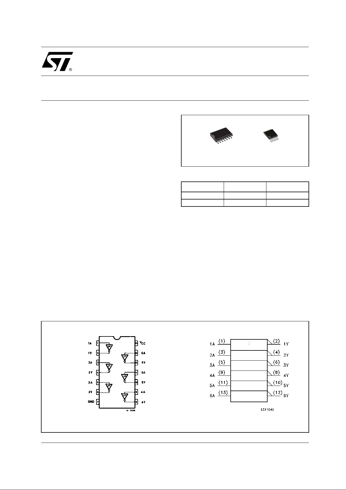
DESCRIPTION
The 74VHC14 is a n advanced high-speed CM OS
HEX SCHMITT INVERTER fabricated with
sub-micron silicon gate and double-layer metal
wiring C
2
MOS technology.
The internal circuit is composed of 3 stages
including buffer output , which enables high noise
immunity and stable output.
Power down protection is provided on all inputs
and 0 to 7V can be accepted on inputs with no
TSSOPSOP
ORDER CODES
PACKAGE TUBE T & R
SOP 74VHC14M 74VHC14MTR
TSSOP 74VHC14TTR
regard to the supply voltage. This device can be
used to interface 5V to 3V.
Pin configuration and function are the same as
those of the 74VHC04 but the 74VHC14 has
hysteresis.
This together with its schmitt trigger function
allows it to be used on line receivers with slow
rise/fall input signals.
All inputs and outputs are equipped with
protection circuits against stat ic discharge, giving
them 2KV ESD immunity and transient excess
voltage.
PIN CONNECTION AND IEC LOGIC SYMBOLS
1/8March 2002
Page 2
74VHC14
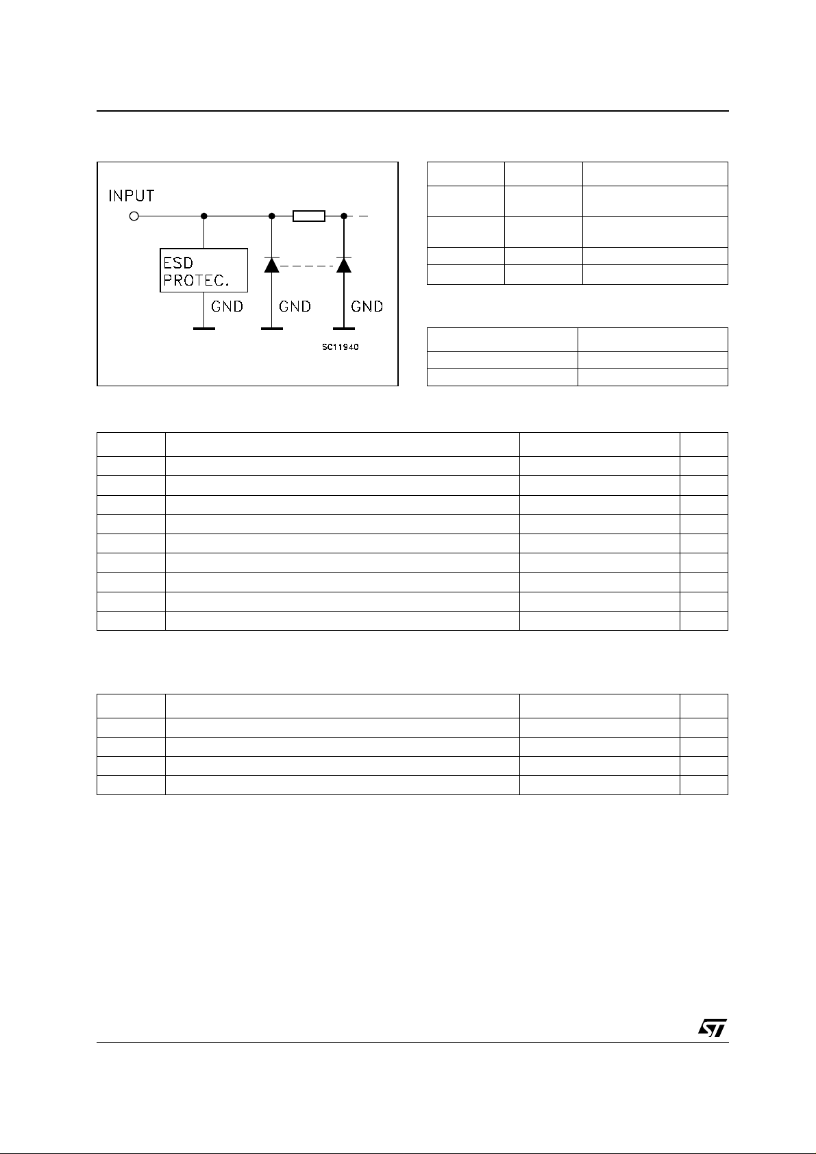
INPUT EQUIVALENT CIRCUIT PIN DESCRIPTION
PIN No SYMBOL NAME AND FUNCTION
1, 3, 5, 9, 1 1,
13
2, 4, 6, 8, 10,
12
7 GND Ground (0V)
14
TRUTH TABLE
ABSOLUTE MAXIMUM RATINGS
Symbol Parameter Value Unit
V
V
V
I
I
OK
I
I
or I
CC
T
T
Absolute Maximum Ratings are those values beyond which damage to the device may occur. Functional operation under these conditions is
not implied
Supply Voltage
CC
DC Input Voltage
I
DC Output Voltage -0.5 to VCC + 0.5
O
DC Input Diode Current
IK
DC Output Diode Current
DC Output Current
O
DC VCC or Ground Current
GND
Storage Temperature
stg
Lead Temperature (10 sec)
L
1A to 6A Data Inputs
1Y to 6Y Data Outputs
V
CC
Positive Supply Voltage
AY
LH
HL
-0.5 to +7.0 V
-0.5 to +7.0 V
V
- 20 mA
20 mA
±
25 mA
±
50 mA
±
-65 to +150 °C
300 °C
RECOMMENDED OPERATING CONDITIONS
Symbol Parameter Value Unit
V
V
V
T
2/8
Supply Voltage
CC
Input Voltage
I
Output Voltage 0 to V
O
Operating Temperature
op
2 to 5.5 V
0 to 5.5 V
CC
-55 to 125 °C
V
Page 3
DC SPECIFICATIONS
Symbol Parameter
V
High Level
t+
Threshold Voltage
Low Level
V
t-
Threshold Voltage
Hysteresis Voltage 3.0 0.3 1.2 0.3 1.2 0.3 1.2
V
h
V
V
I
High Level Output
OH
Voltage
Low Level Output
OL
Voltage
I
Input Leakage
I
Current
Quiescent Supply
CC
Current
74VHC14
Test Condition Value
T
= 25°C
V
CC
(V)
A
Min. Typ. Max. Min. Max. Min. Max.
3.0 1.2 2.2 1.2 2.2 1.2 2.2
5.5 2.15 3.85 2.15 3.85 2.15 3.85
3.0 0.9 1.9 0.9 1.9 0.9 1.9
5.5 1.65 3.35 1.65 3.35 1.65 3.35
5.5 0.5 1.6 0.5 1.6 0.5 1.6
=-50 µA
2.0
3.0
4.5
3.0
4.5
2.0
3.0
4.5
3.0
4.5
0 to
5.5
5.5
I
O
I
=-50 µA
O
I
=-50 µA
O
I
=-4 mA
O
I
=-8 mA
O
IO=50 µA
I
=50 µA
O
I
=50 µA
O
I
=4 mA
O
I
=8 mA
O
V
= 5.5V or GND
I
= VCC or GND
V
I
1.9 2.0 1.9 1.9
2.9 3.0 2.9 2.9
4.4 4.5 4.4 4.4
2.58 2.48 2.4
3.94 3.8 3.7
0.0 0.1 0.1 0.1
0.0 0.1 0.1 0.1
0.0 0.1 0.1 0.1
-40 to 85°C -55 to 125°C
0.36 0.44 0.55
0.36 0.44 0.55
±
0.1
1
±
±
22020
Unit
1
V4.5 1.75 3.15 1.75 3.15 1.75 3.15
V4.5 1.35 2.75 1.35 2.75 1.35 2.75
V4.5 0.4 1.4 0.4 1.4 0.4 1.4
V
V
A
µ
A
µ
AC ELECTRICAL CHARACTERISTICS (Input t
Test Condition Value
Symbol Parameter
t
PLH
t
PHL
(*) Vol tage range is 3.3V
(**) Voltage range is 5.0V
Propagation Delay
Time
±
0.3V
0.5V
±
3.3
3.3
5.0
5.0
C
V
CC
(V)
L
(pF)
(*)
15 8.3 12.8 1.0 15.0 1.0 15.0
(*)
50 10.8 16.3 1.0 18.5 1.0 18.5
(**)
15 5.5 8.6 1.0 10.0 1.0 10.0
(**)
50 7.0 10.6 1.0 12.0 1.0 12.0
= tf = 3ns))
r
= 25°C
T
A
-40 to 85°C -55 to 125°C
Min. Typ. Max. Min. Max. Min. Max.
Unit
ns
3/8
Page 4

74VHC14
CAPACITIVE CHARACTERISTICS
Test Condition Value
= 25°C
Symbol Parameter
T
A
Min. Typ. Max. Min. Max. Min. Max.
C
C
Input Capacitance
IN
Power Dissipation
PD
Capacitance
6101010pF
14 pF
(note 1)
1) CPD is defined as the value of the IC’s internal equivalent capacitance which is calculated from the operating current consumption without
load. (Refer to Test Circuit). Average operating current can be obtained by the following equation. I
DYNAMIC SWITCHING CHARACTERISTICS
Test Condition Value
= 25°C
Symbol Parameter
V
CC
(V)
V
V
Dynamic Low
OLP
Voltage Quiet
OLV
Output (note 1, 2)
5.0
Dynamic High
C
V
IHD
Voltage Input
5.0 3.5 V
= 50 pF
L
(note 1, 3)
Dynamic Low
V
ILD
Voltage Input
5.0 1.5 V
(note 1, 3)
1) Worst c ase package.
2) Max number of output s defined as (n). Data inputs ar e driven 0V to 5.0V, (n-1) outputs switchin g and one output at GND.
3) Max number of data inputs (n) switching. (n-1) switching 0V to 5.0V. Inputs under test switching: 5.0V to threshold (V
(V
), f=1MHz.
IHD
T
A
Min. Typ. Max. Min. Max. Min. Max.
0.3 0.8
-0.8 -0.3
-40 to 85°C -55 to 125°C
= CPD x VCC x fIN + ICC/6 (per gate)
CC(opr)
-40 to 85°C -55 to 125°C
), 0V to threshold
ILD
Unit
Unit
V
TEST CIRCUIT
CL =15/50pF or equivalent (includes jig an d probe capaci ta nce)
R
= Z
of pulse generator (typically 50Ω)
T
OUT
4/8
Page 5

WAVEFORM: PROPAGATION DELAYS (f=1MHz; 50% duty cycle)
74VHC14
5/8
Page 6

74VHC14
SO-14 MECHANICAL DATA
DIM.
A 1.75 0.068
a1 0.1 0.2 0.003 0.007
a2 1.65 0.064
b 0.35 0.46 0.013 0.018
b1 0.19 0.25 0.007 0.010
C 0.5 0.019
c1 45° (typ.)
D 8.55 8.75 0.336 0.344
E 5.8 6.2 0.228 0.244
e 1.27 0.050
e3 7.62 0.300
F 3.8 4.0 0.149 0.157
G 4.6 5.3 0.181 0.208
L 0.5 1.27 0.019 0.050
M 0.68 0.026
S8° (max.)
MIN. TYP MAX. MIN. TYP. M AX.
mm. inch
6/8
PO13G
Page 7

74VHC14
TSSOP14 MECHANICAL DATA
mm. inch
DIM.
MIN. TYP MAX. MIN. TYP. M AX.
A 1.2 0.047
A1 0.05 0.15 0.002 0.004 0.006
A2 0.8 1 1.05 0.031 0.039 0.041
b 0.19 0.30 0.007 0.012
c 0.09 0.20 0.004 0.0089
D 4.9 5 5.1 0.193 0.197 0.201
E 6.2 6.4 6.6 0.244 0.252 0.260
E1 4.3 4.4 4.48 0.169 0.173 0.176
e 0.65 BSC 0.0256 BSC
K0° 8°0° 8°
L 0.45 0.60 0.75 0.018 0.024 0.030
A2
A
A1
b
e
c
K
L
E
D
E1
PIN 1 IDENTIFICATION
1
0080337D
7/8
Page 8

74VHC14
Information furnished is believed to be accurate and reliable. However, STMicroelectronics assumes no responsibility f or the
consequences of use of such informatio n nor for any infringement of paten ts or o ther rig hts of t hird part ies which ma y result from
its use. No license is granted by implication or otherwise under any patent or patent rights of STMicroelectronics. Specifications
mentioned in this publication are subject to change without notice. This publication supersedes and replaces all information
previousl y suppl ied. STM icroel ectronics produc ts are not auth orized for use as c ritica l compone nts in l ife s upport dev ices or
systems without express written approval of STMicroelectronics.
Australia - Brazil - Canada - China - Finland - France - Germany - Hong Kong - India - Israel - Italy - Japan - Malaysia - Malta - Morocco
© The ST logo is a registered trademark of STMicroelectronics
© 2002 STMicroelectronics - Prin ted in Italy - All Rights Reserved
STMicroelectronics GROUP OF COMPANIES
Singapore - Spain - Sweden - Switzerland - United Kingdom - United States.
© http://www.st.com
8/8
 Loading...