

Datasheet 74VHC139SJX, 74VHC139SJ, 74VHC139CW, 74VHC139N, 74VHC139MX Datasheet (Fairchild Semiconductor)
...Page 1
November 1992
Revised April 1999
74VHC139 Dual 2-to-4 Decoder/Demultiplexer
© 1999 Fairchild Semiconductor Corporation DS011521.prf www.fairchildsemi.com
74VHC139
Dual 2-to-4 Decoder/Demultiplexer
General Description
The VHC139 is an adva nced hig h sp eed C MO S D ua l 2-t o4 Decoder/Demultiplexer fabricated with silicon gate
CMOS technology. It achieves the high speed operation
similar to equivalent Bipolar Schottky TTL while maintaining the CMOS low power dissipation.
The active LOW enable input ca n be used for gating or it
can be used as a data input for demultiplexing applications.
When the enable input is held HIGH, all four outputs are
fixed at a HIGH logic level inde pen de nt of the other inputs.
An input protection circuit en sures that 0V to 7V can be
applied to the input pins without re gard to the supply volt-
age. This device can be used to interface 5V to 3V systems
and two supply systems such as ba ttery back up . This circuit prevents device destruction due to m isma tche d supply
and input voltages.
Features
■ High Speed: tPD = 5.0 ns (typ) at TA = 25°C
■ Low power dissipation: I
CC
= 4 µA (Max.) at TA = 25°C
■ High noise immunity: V
NIH
= V
NIL
= 28% VCC (Min.)
■ Power down protection is provided on all inputs
■ Pin and function compatible with 74HC139
Ordering Code:
Surface mount pack ages are also available on Tape and Reel. Specify by appending the s uffix let te r “X” to the ordering code.
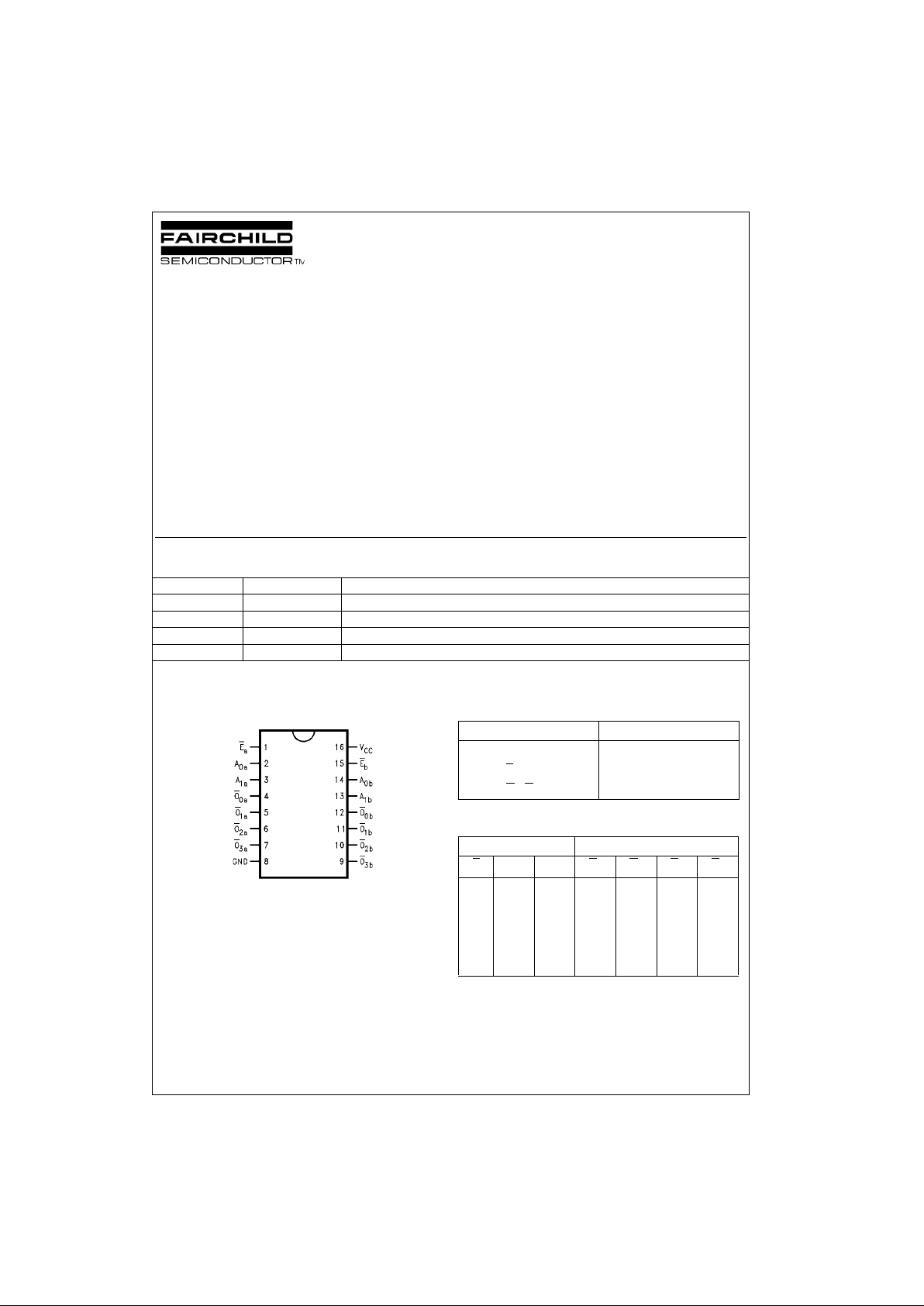
Connection Diagram Pin Description
Truth Table
H = HIGH Voltage Level
L = LOW Voltage Level
X = Immaterial
Order Number Package Number Package Description
74VHC139M M16A 16-Lead Small Outline Integrated Circuit (SOIC), JEDEC MS-012, 0.150” Narrow
74VHC139SJ M16D 16-Lead Small Outline Package (SOP), EIAJ TYPE II, 5.3mm Wide
74VHC139MTC MTC16 16-Lead Thin Shrink Small Outline Package (TSSOP), JEDEC MO-153, 4.4mm Wide
74VHC139N N16E 16-Lead Plastic Dual-In-Line Package (PDIP), JEDEC MS-001, 0.300” Wide
Pin Names Description
A
0
, A
1
Address Inputs
E
Enable Inputs
O
0–O3
Outputs
Inputs Outputs
E
A
0
A
1
O
0
O
1
O
2
O
3
HXXHHHH
LLLLHHH
LHLHLHH
LLHHHLH
LHHHHHL
Page 2
www.fairchildsemi.com 2
74VHC139
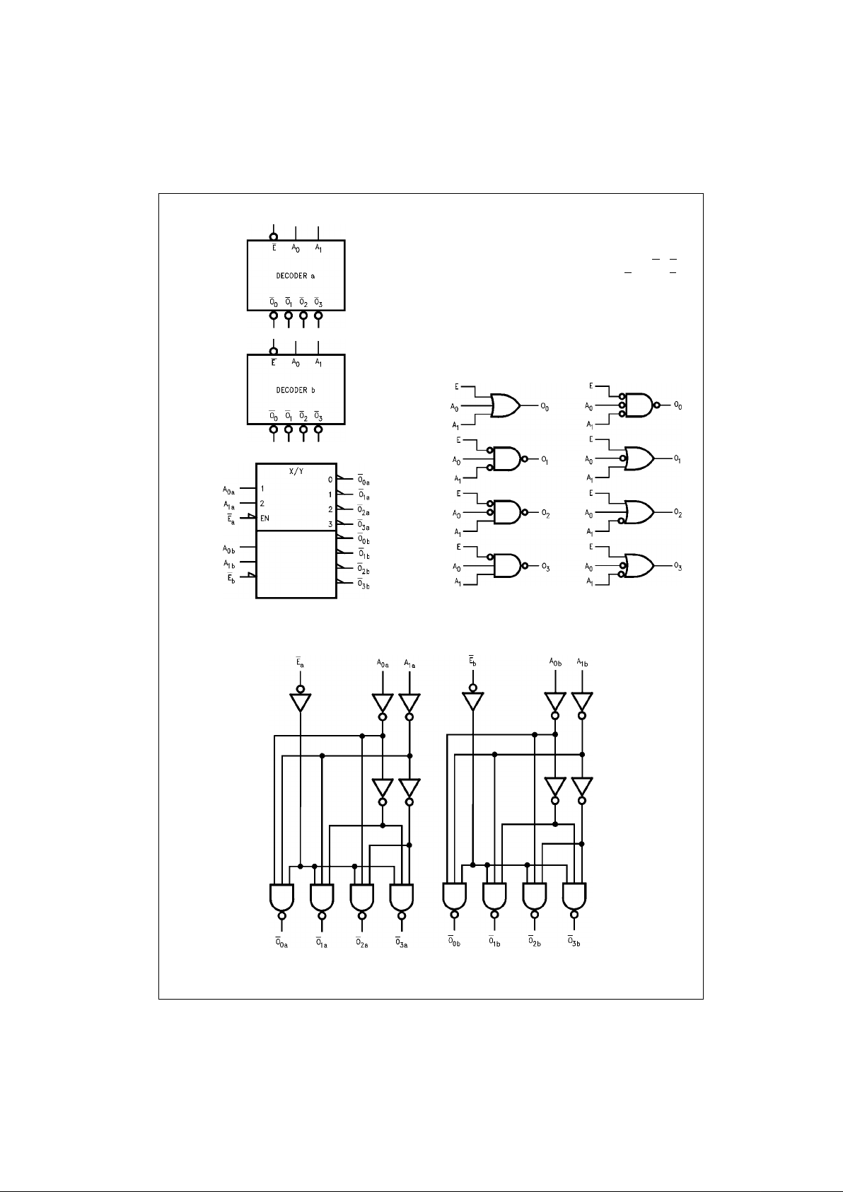
Logic Symbols
IEEE/IEC
Functional Description
The VHC139 is a high-spe ed dual 2-to-4 de coder/demul tiplexer. The device has two independent decode rs, each of
which accepts two binary weighted inputs (A
0–A1
) and pro-
vides four mutually exclusive active-LOW outputs (O
0–O3
).
Each decoder has an active-LOW enable (E
). When E is
HIGH all outputs are forced HIGH. The enable can be used
as the data input for a 4-output demu ltiplexer applicat ion.
Each half of the VHC1 39 generates all four minterms of
two variables. These four minterms are useful in some
applications, replacin g multip le gate fun ctions as sho wn in
Figure 1
, and thereby reduc ing the number of packages
required in a logic network.
FIGURE 1. Gate Functions (Each Half)
Logic Diagram
Please note that this diagram is provided only f or t he understanding of logic operations and should not be used to estimate propagation delays.
Page 3

3 www.fairchildsemi.com
74VHC139
Absolute Maximum Ratings(Note 1) Recommended Operating
Conditions
(Note 2)
Note 1: Absolute Maximum Ratings are valu es beyond whic h the device
may be damaged or ha ve its useful life impaire d. The datab ook specifications should be met, without exception, to ensure that the system design is
reliable over its p ower supp ly, temperature, and o utput/input loading variables. Fairchild does not recommend operation outside databook specifications.
Note 2: Unused inputs must be held HIGH or LOW. They may not float.
DC Electrical Characteristics
AC Electrical Characteristics
Note 3: CPD is defined as the value of the internal equiv alent capacitance which is calculated from the operating current c ons umption without load. Average
operating current ca n be obtained by the equat ion: I
CC
(opr.) = CPD * VCC * fIN + ICC/2 (per decoder).
Supply Voltage (VCC) −0.5V to +7.0V
DC Input Voltage (V
IN
) −0.5V to +7.0V
DC Output Voltage (V
OUT
) −0.5V to VCC + 0.5V
Input Diode Current (I
IK
) −20 mA
Output Diode Current (I
OK
) ±20 mA
DC Output Current (I
OUT
) ±25 mA
DC V
CC
/GND Current (ICC) ±75 mA
Storage Temperature (T
STG
) −65°C to +150°C
Lead Temperature (T
L
)
(Soldering, 10 seconds) 260°C
Supply Voltage (V
CC
)2.0V to +5.5V
Input Voltage (V
IN
)0V to +5.5V
Output Voltage (V
OUT
)0V to V
CC
Operating Temperature (T
OPR
) −40°C to +85°C
Input Rise and Fall Time (t
r
, tf)
V
CC
= 3.3V ± 0.3V 0 ∼ 100 ns/V
V
CC
= 5.0V ± 0.5V 0 ∼ 20 ns/V
Symbol Parameter
V
CC
(V)
TA = 25°CT
A
= −40°C to +85°C
Units Conditions
Min Typ Max Min Max
V
IH
HIGH Level 2.0 1.50 1.50
V
Input Voltage 3.0 − 5.5 0.7 V
CC
0.7 V
CC
V
IL
LOW Level 2.0 0.50 0.50
V
Input Voltage 3.0 − 5.5 0.3 V
CC
0.3 V
CC
V
OH
HIGH Level 2.0 1.9 2.0 1.9 VIN = VIHIOH = −50 µA
Output Voltage 3.0 2.9 3.0 2.9 V or V
IL
4.5 4.4 4.5 4.4
3.0 2.58 2.48
V
IOH = −4 mA
4.5 3.94 3.80 IOH = −8 mA
V
OL
LOW Level 2.0 0.0 0.1 0.1 VIN = VIHIOL = 50 µA
Output Voltage 3.0 0.0 0.1 0.1 V or V
IL
4.5 0.0 0.1 0.1
3.0 0.36 0.44
V
IOL = 4 mA
4.5 0.36 0.44 IOL = 8 mA
I
IN
Input Leakage Current 0 − 5.5 ±0.1 ±1.0 µAVIN = 5.5V or GND
I
CC
Quiescent Supply Current 5.5 4.0 40.0 µAVIN = VCC or GND
Symbol Parameter
V
CC
(V)
TA = 25°CT
A
= −40°C to +85°C
Units Conditions
Min Typ Max Min Max
t
PLH
Propagation Delay 3.3 ± 0.3 7.2 11.0 1.0 13.0
ns
CL = 15 pF
t
PHL
Anto O
n
9.7 14.5 1.0 16.5 CL = 50 pF
5.0 ± 0.5 5.0 7.2 1.0 8.5
ns
CL = 15 pF
6.5 9.2 1.0 10.5 CL = 50 pF
t
PLH
Propagation Delay 3.3 ± 0.3 6.4 9.2 1.0 11.0
ns
CL = 15 pF
t
PHL
Ento O
n
8.9 12.7 1.0 14.5 CL = 50 pF
5.0 ± 0.5 4.4 6.3 1.0 7.5
ns
CL = 15 pF
5.98.31.09.5 C
L
= 50 pF
C
IN
Input Capacitance 4 10 10 pF VCC = Open
C
PD
Power Dissipation Capacitance 26 pF (Note 3)
Page 4

www.fairchildsemi.com 4
74VHC139
Physical Dimensions inches (millimeters) unless otherwise noted
16-Lead Small Outline Integrated Circuit (SOIC), JEDEC MS-012, 0.150” Narrow
Package Number M16A
16-Lead Small Outline Package (SOP), EIAJ TYPE II, 5.3mm Wide
Package Number M16D
Page 5

5 www.fairchildsemi.com
74VHC139
Physical Dimensions inches (millimeters) unless otherwise noted (Continued)
16-Lead Thin Shrink Small Outline Package (TSSOP), JEDEC MO-153, 4.4mm Wide
Package Number MTC16
Page 6

Fairchild does not assume any responsibility for use of any circuitry described, no circuit patent licenses are implied and Fairchild reserves the right at any time without notice to change said circuitry and specifications.
74VHC139 Dual 2-to-4 Decoder/Demultiplexer
LIFE SUPPORT POLICY
FAIRCHILD’S PRODUCTS ARE NOT AUTHORIZED FOR USE AS CRITICAL COMPONENTS IN LIFE SUPPORT
DEVICES OR SYSTEMS WITHOUT THE EXPRESS WRITTEN APPROVAL OF THE PRESIDENT OF FAIRCHILD
SEMICONDUCTOR CORPORATION. As used herein:
1. Life support devices or systems are devices or syste ms
which, (a) are intended for surgical implant into the
body, or (b) support or sustain life, and (c) whose failure
to perform when properly used in accordance with
instructions for use provided in the labeling, can be reasonably expected to result in a significant inju ry to the
user.
2. A critical component i n any compon ent of a lif e support
device or system whose failu re to perform can be reasonably expected to ca use the fa i lure of the life su pp ort
device or system, or to affect its safety or effectiveness.
www.fairchildsemi.com
Physical Dimensions inches (millimeters) unless otherwise noted (Continued)
16-Lead Plastic Dual-In-Line Package (PDIP), JEDEC MS-001, 0.300” Wide
Package Number N16E
 Loading...