

Page 1
74VHC139
DUAL 2 TO 4 DECODER/DEMULTIPLEXER
■ HIGHSPEED:t
■ LOW POWER DISSIPATION:
=4 µA (MAX.) at TA=25oC
I
CC
■ HIGHNOISEIMMUNITY:
V
NIH=VNIL
■ POWERDOWNPROTECTIONON INPUTS
■ SYMMETRICALOUTPUTIMPEDANCE:
|=IOL=8 mA(MIN)
|I
OH
■ BALANCEDPROPAGATIONDELAYS:
t
≅ t
PLH
■ OPERATINGVOLTAGERANGE:
V
(OPR)= 2Vto 5.5V
CC
■ PINANDFUNCTIONCOMPATIBLEWITH
=28%VCC(MIN.)
PHL
=5.0ns (TYP.)atVCC=5V
PD
74SERIES139
■ IMPROVEDLATCH-UPIMMUNITY
DESCRIPTION
The 74VHC139 is an advanced high-speed
CMOS DUAL 2 TO 4 LINE DECODER/
DEMULTIPLEXER fabricated with sub-micron
silicon gate and double-layermetal wiring C
2
MOS
technology.
The active low enable input can be used for
M1
(Micro Package)
(TSSOPPackage)
T
ORDERCODES :
74VHC139M 74VHC139T
gating or as a data input for demultiplexing
applications. While the enable input is held high,
all four outputs are high independently of the
other inputs.
Power down protection is provided on all inputs
and 0 to 7V can be accepted on inputs with no
regard to the supply voltage. This device can be
used to interface 5V to 3V.
All inputs and outputs are equipped with
protection circuits against static discharge, giving
them 2KV ESD immunity and transient excess
voltage.
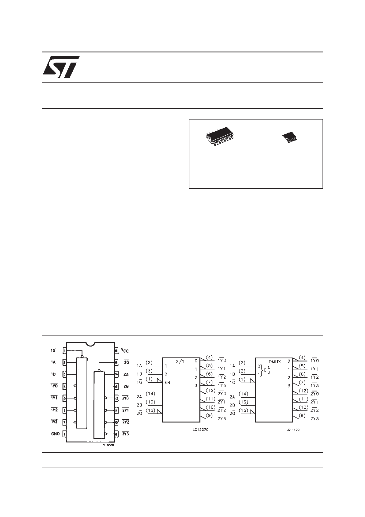
PIN CONNECTION AND IEC LOGIC SYMBOLS
June 1999
1/8
Page 2
74VHC139
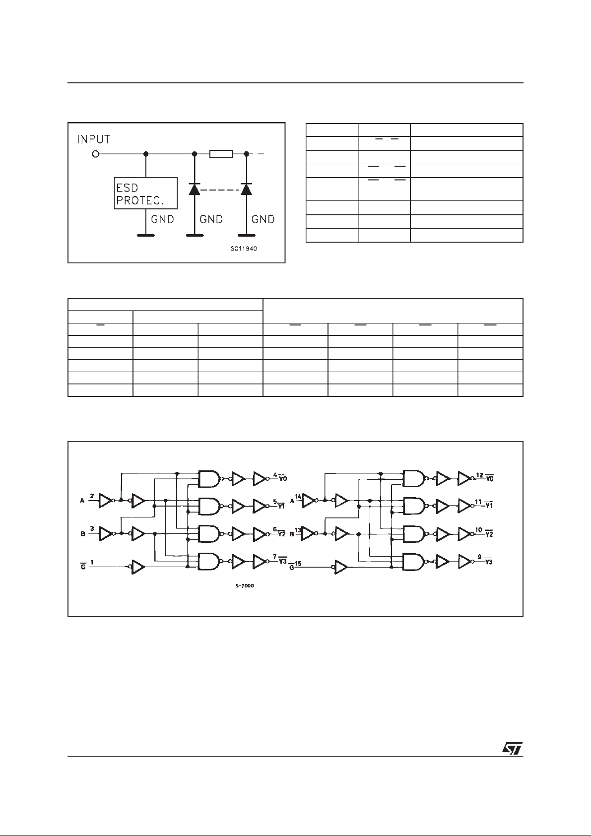
INPUT EQUIVALENTCIRCUIT
PIN DESCRIPTION
PI N No SYM BO L NAM E AND FU NCTIO N
1, 15 1G, 2G Enable Inputs
2, 3 1A, 1B Address Inputs
4, 5, 6,7 1Y0 to 1Y3 Outputs
12, 11, 10,92Y0 to 2Y3 Outputs
14, 13 2A, 2B Address Inputs
8 GND Ground (0V)
16 V
CC
Positive Supply Voltage
TRUTH TABLE
INPUTS OUTPUTS
ENABLE SELECT
G B A Y0Y1Y2Y3
HXXHHHH
LLLLHHH
LLHHLHH
LHLHHLH
X:Don’tCare
LHHHHHL
LOGICDIAGRAM
Thislogic diagram has notbe used to estimate propagation delays
2/8
Page 3
74VHC139
ABSOLUTE MAXIMUM RATINGS
Symb o l Para met er Val u e Uni t
V
V
V
I
I
OK
I
or I
I
CC
T
T
AbsoluteMaximumRatingsarethosevaluesbeyondwhichdamage tothedevicemayoccur. Functionaloperationunderthese condition isnotimplied.
RECOMMENDEDOPERATINGCONDITIONS
Symb o l Para met er Value Un it
V
V
V
T
dt/dv
1)VINfrom30%to70%of V
Supply Voltage -0.5 to +7.0 V
CC
DC Input Voltage -0.5 to +7.0 V
I
DC Output Voltage -0.5 to VCC+ 0.5 V
O
DC Input Diode Current - 20 mA
IK
DC Output Diode Current ± 20 mA
DC Output Current
O
DC VCCor Ground Current
GND
Storage Temperature -65 to +150
stg
Lead Temperature (10 sec) 300
L
Supply Voltage 2.0 to 5.5 V
CC
Input Voltage 0 to 5.5 V
I
Output Voltage 0 to V
O
Operating Temperature -40 to +85
op
(V
CC
CC
=3.3±0.3V)
=5.0±0.5V)
Input Rise and Fall Time (see note 1) (V
CC
25 mA
±
75 mA
±
CC
0 to 100
0to20
o
C
o
C
V
o
C
ns/V
ns/V
DC SPECIFICATIONS
Symb o l Parameter Test C o n dit i ons Val u e Uni t
=25oC -40 to 85oC
V
CC
(V)
High Level Input
V
IH
Voltage
V
Low Level Input
IL
Voltage
V
High Level Output
OH
Voltage
Low Level Output
V
OL
Voltage
Input Leakage Current 0 to 5.5 VI= 5.5V or GND ±0.1 ±1.0 µA
I
I
Quiescent Supply
I
CC
2.0 1.5 1.5
3.0 to 5.5 0.7V
2.0 0.5 0.5
3.0 to 5.5 0.3V
2.0 IO=-50 µA 1.9 2.0 1.9
3.0 I
4.5 I
3.0 I
4.5 I
=-50 µA 2.9 3.0 2.9
O
=-50µA 4.4 4.5 4.4
O
=-4 mA 2.58 2.48
O
=-8 mA 3.94 3.8
O
2.0 IO=50 µA 0.0 0.1 0.1
3.0 I
4.5 I
3.0 I
4.5 I
=50 µA 0.0 0.1 0.1
O
=50µA 0.0 0.1 0.1
O
=4 mA 0.36 0.44
O
=8 mA 0.36 0.44
O
5.5 VI=VCCorGND 4 40 µA
Current
T
A
Min. Typ. Max. Min. Max.
CC
0.7V
CC
0.3V
CC
CC
V
V
V
V
3/8
Page 4

74VHC139
AC ELECTRICAL CHARACTERISTICS
(Inputt
r=tf
=3 ns)
Symbol P arameter Test Condition Value Unit
t
Propagation Delay
PLH
t
Time
PHL
A, B, to Y
t
Propagation Delay
PLH
t
Time
PHL
GtoY
(*) Voltagerangeis 3.3V± 0.3V
(**) Voltagerangeis 5V± 0.5V
V
3.3
3.3
5.0
5.0
3.3
3.3
5.0
5.0
CC
(V)
(**)
(**)
(**)
(**)
C
L
(pF)
(*)
15 7.2 11.0 1.0 13.0
(*)
50 9.7 14.5 1.0 16.5
T
=25oC -40 to 85oC
A
Min. Typ. Max. Min. Max.
15 5.0 7.2 1.0 8.5
50 6.5 9.2 1.0 10.5
(*)
15 6.4 9.2 1.0 11.0
(*)
50 8.9 12.7 1.0 14.5
15 4.4 6.3 1.0 7.5
50 5.9 8.3 1.0 9.5
ns
ns
CAPACITIVE CHARACTERISTICS
Symb o l Parameter Test C o n dit i ons Val u e Uni t
=25oC -40 to 85oC
T
A
Min. Typ. Max. Min. Max.
Input Capacitance 4 10 10
C
IN
Power Dissipation
C
PD
26 pF
Capacitance (note 1)
1)CPDisdefinedasthevalue oftheIC’sinternalequivalentcapacitance whichis calculated fromtheoperating currentconsumption withoutload.(Referto
TestCircuit).Averageoperatingcurrent canbeobtainedbythefollowingequation.I
(opr)= CPD• VCC• fIN+ICC/2(perDecoder)
CC
pF
TESTCIRCUIT
CL= 15/50 pF or equivalent (includes jigand probe capacitance)
R
ofpulse generator (typically50Ω)
T=ZOUT
4/8
Page 5

74VHC139
WAVEFORM1: PROPAGATIONDELAYS FOR INVERTING OUTPUTS(f=1MHz;50% duty cycle)
WAVEFORM2: PROPAGATIONDELAYS FOR NON-INVERTING OUTPUTS(f=1MHz;50%dutycycle)
5/8
Page 6

74VHC139
SO-16 MECHANICAL DATA
DIM.
MIN. TYP. MAX. MIN. TYP. MAX.
A 1.75 0.068
a1 0.1 0.2 0.004 0.007
a2 1.65 0.064
b 0.35 0.46 0.013 0.018
b1 0.19 0.25 0.007 0.010
C 0.5 0.019
c1 45 (typ.)
D 9.8 10 0.385 0.393
E 5.8 6.2 0.228 0.244
e 1.27 0.050
e3 8.89 0.350
F 3.8 4.0 0.149 0.157
G 4.6 5.3 0.181 0.208
L 0.5 1.27 0.019 0.050
M 0.62 0.024
S 8 (max.)
mm inch
6/8
P013H
Page 7

TSSOP16 MECHANICAL DATA
74VHC139
DIM.
mm inch
MIN. TYP. MAX. MIN. TYP. MAX.
A 1.1 0.433
A1 0.05 0.10 0.15 0.002 0.004 0.006
A2 0.85 0.9 0.95 0.335 0.354 0.374
b 0.19 0.30 0.0075 0.0118
c 0.09 0.20 0.0035 0.0079
D 4.9 5 5.1 0.193 0.197 0.201
E 6.25 6.4 6.5 0.246 0.252 0.256
E1 4.3 4.4 4.48 0.169 0.173 0.176
e 0.65 BSC 0.0256BSC
K0
o
o
4
o
8
o
0
o
4
L 0.50 0.60 0.70 0.020 0.024 0.028
o
8
A2
A
A1
PIN 1 IDENTIFICATION
b
e
c
K
L
E
D
E1
1
7/8
Page 8

74VHC139
Information furnished is believed to beaccurate and reliable. However, STMicroelectronics assumes no responsibility fortheconsequences
of use of such information nor for any infringement of patents or other rights of third parties which may result from its use. No license is
granted by implication or otherwise under any patent or patent rights of STMicroelectronics. Specification mentioned in this publication are
subject tochange without notice. Thispublication supersedes and replaces all information previously supplied. STMicroelectronics products
are not authorized for use as critical components in life support devices or systems without express written approval of STMicroelectronics.
The ST logo is a trademark of STMicroelectronics
1999 STMicroelectronics – Printed in Italy – All Rights Reserved
STMicroelectronics GROUP OF COMPANIES
Australia - Brazil - Canada - China -France -Germany - Italy - Japan - Korea - Malaysia - Malta - Mexico - Morocco - The Netherlands -
Singapore - Spain -Sweden - Switzerland - Taiwan - Thailand - UnitedKingdom - U.S.A.
http://www.st.com
.
8/8
 Loading...