

Page 1
QUAD BUS BUFFERS (3-STATE)
■ HIGHSPEED:t
■ LOW POWER DISSIPATION:
I
=4 µA (MAX.) at TA=25oC
CC
■ HIGHNOISEIMMUNITY:
V
NIH=VNIL
■ POWERDOWNPROTECTIONON INPUTS
■ SYMMETRICALOUTPUTIMPEDANCE:
|I
|=IOL=8 mA(MIN)
OH
■ BALANCEDPROPAGATIONDELAYS:
≅ t
t
PLH
■ OPERATINGVOLTAGERANGE:
V
(OPR)= 2Vto 5.5V
CC
■ PINANDFUNCTION COMPATIBLEWITH
=28%VCC(MIN.)
PHL
74SERIES126
■ IMPROVEDLATCH-UP IMMUNITY
■ LOWNOISE:V
DESCRIPTION
The 74VHC126 is an advanced high-speed
CMOS QUAD BUS BUFFERS fabricated with
sub-micron silicon gate and double-layer metal
wiringC
2
MOStechnology.
=3.8ns(TYP.)atVCC=5V
PD
= 0.8V(Max.)
OLP
74VHC126
PRELIMINARY DATA
M
(Micro Package)
(TSSOPPackage)
ORDERCODES :
74VHC126M 74VHC126T
This device requires the 3-STATEcontrol input G
to be set low to place the output into the high
impedancestate.
Power down protection is provided on all inputs
and 0 to 7V can be accepted on inputs with no
regard to the supply voltage. This device can be
used to interface5V to 3V.
All inputs and outputs are equipped with
protection circuits against static discharge, giving
them 2KV ESD immunity and transient excess
voltage.
T
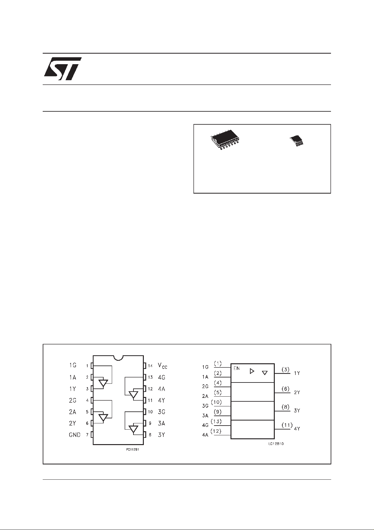
PIN CONNECTION AND IECLOGIC SYMBOLS
June 1999
1/8
Page 2
74VHC126
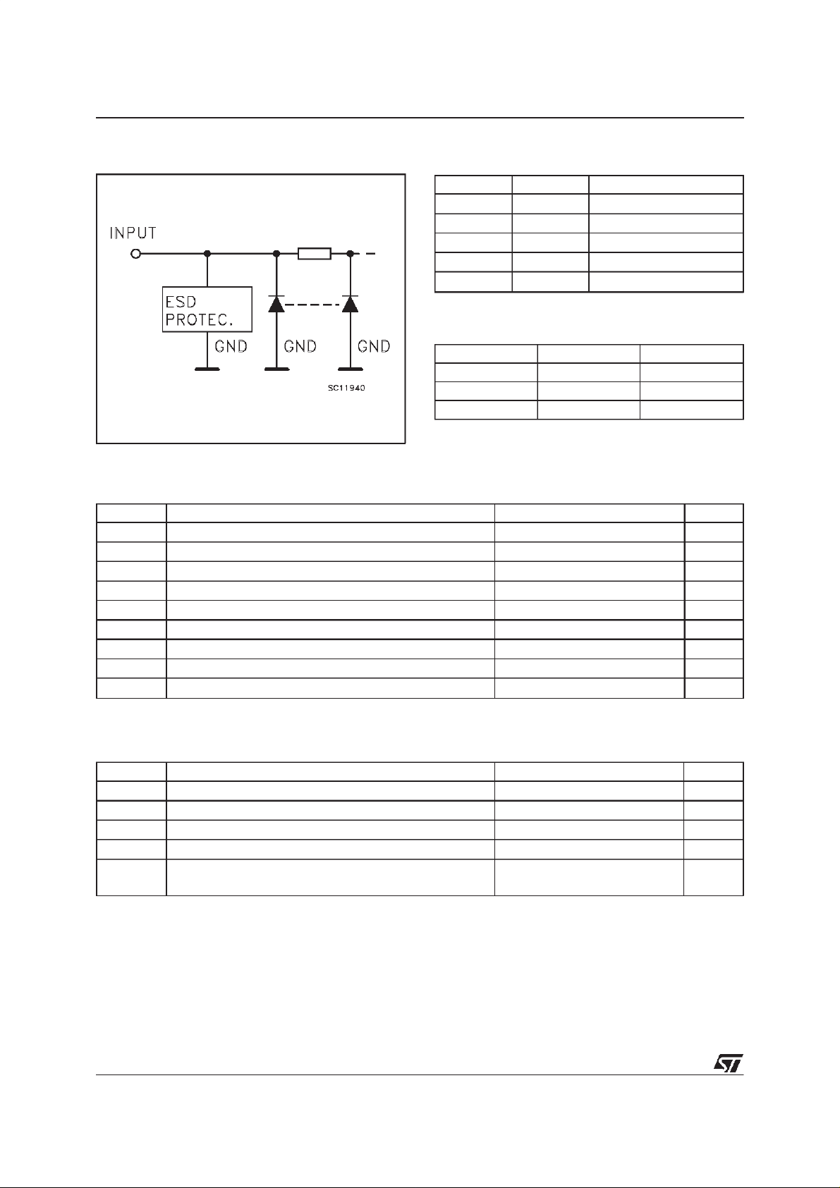
INPUT EQUIVALENTCIRCUIT
PIN DESCRIPTION
PI N No SYMB OL NAME AND FU NCTION
1, 4, 10, 13 1G to 4G Output Enable Inputs
2, 5, 9, 12 1A to 4A Data Inputs
3, 6, 8, 11 1Y to 4Y Data Outputs
7 GND Ground (0V)
14 V
CC
Positive Supply Voltage
TRUTH TABLE
AGY
XLZ
LHL
HHH
X:”H” or”L”
Z: HighImpedance
ABSOLUTE MAXIMUMRATINGS
Symb o l Para met er Val u e Uni t
V
V
V
I
I
OK
I
or I
I
CC
T
T
AbsoluteMaximumRatingsarethosevalues beyond whichdamagetothedevicemayoccur. Functionaloperationundertheseconditionisnotimplied.
Supply Voltage -0.5 to +7.0 V
CC
DC Input Voltage -0.5 to +7.0 V
I
DC Output Voltage -0.5 to VCC+ 0.5 V
O
DC Input Diode Current - 20 mA
IK
DC Output Diode Current ± 20 mA
DC Output Current ± 25 mA
O
DC VCCor Ground Current ± 50 mA
GND
Storage Temperature -65 to +150
stg
Lead Temperature (10 sec) 300
L
o
C
o
C
RECOMMENDEDOPERATINGCONDITIONS
Symb o l Para met er Value Un it
V
V
V
T
dt/dv
1)VINfrom30%to70%of V
2/8
Supply Voltage 2.0 to 5.5 V
CC
Input Voltage 0 to 5.5 V
I
Output Voltage 0 to V
O
Operating Temperature -40 to +85
op
(V
CC
CC
=3.3±0.3V)
=5.0±0.5V)
Input Rise and Fall Time (see note 1) (V
CC
CC
0 to 100
0to20
V
o
C
ns/V
ns/V
Page 3
74VHC126
DC SPECIFICATIONS
Symb o l Para meter Test C o n ditio ns Val u e Uni t
T
V
CC
(V)
High Level Input
V
IH
Voltage
V
Low Level Input
IL
Voltage
V
High Level Output
OH
Voltage
2.0 1.5 1.5
3.0 to 5.5 0.7V
2.0 0.5 0.5
3.0 to 5.5 0.3V
2.0 IO=-50µA 1.9 2.0 1.9
3.0 I
4.5 I
3.0 I
4.5 I
Low Level Output
V
OL
Voltage
2.0 IO=50µA 0.0 0.1 0.1
3.0 I
4.5 I
3.0 I
4.5 I
High Impedance
I
OZ
Output Leakage
5.5
VO=VCCor GND
Current
Input Leakage Current 0 to 5.5 VI= 5.5V or GND
I
I
Quiescent Supply
I
CC
5.5 VI=VCCorGND 4 40
Current
Min. Typ. Max. Min. Max.
=-50µA 2.9 3.0 2.9
O
=-50µA 4.4 4.5 4.4
O
=-4 mA 2.58 2.48
O
=-8 mA 3.94 3.8
O
=50µA 0.0 0.1 0.1
O
=50µA 0.0 0.1 0.1
O
=4 mA 0.36 0.44
O
=8 mA 0.36 0.44
O
VI=VIHor V
IL
=25oC -40 to 85oC
A
±
±
0.7V
CC
0.25
0.1
CC
CC
0.3V
±
±
2.5
1.0
CC
µ
µ
µ
V
V
V
V
A
A
A
AC ELECTRICAL CHARACTERISTICS (Input tr=tf=3 ns)
Symbol Parameter Test Condition Value Unit
t
Propagation Delay
PLH
t
Time
PHL
t
Output Disable Time 3.3
PLZ
t
PHZ
Output Enable Time 3.3
t
PZL
t
PZH
(*) Voltagerangeis3.3V± 0.3V
(**) Voltagerangeis 5V± 0.5V
V
3.3
3.3
5.0
5.0
3.3
5.0
5.0
5.0
CC
(V)
(**)
(**)
(**)
(**)
(**)
C
L
(pF)
(*)
15 5.6 8.0 1.0 9.5
(*)
50 8.1 11.5 1.0 13.0
T
=25oC -40 to 85oC
A
Min. Typ. Max. Min. Max.
15 3.8 5.5 1.0 6.5
50 5.3 7.5 1.0 8.5
(*)
(*)
15 RL=1K
50 RL=1K
Ω
Ω
5.4 8.0 1.0 9.5
7.9 11.5 1.0 13.0
15 RL=1KΩ 3.6 5.1 1.0 6.0
50 RL=1K
(*)
50 RL=1KΩ 9.5 13.2 1.0 15.0
50 RL=1K
Ω
Ω
5.1 7.1 1.0 8.0
6.1 8.8 1.0 10.0
ns
ns
ns
3/8
Page 4

74VHC126
CAPACITIVE CHARACTERISTICS
Symbol Parameter Test Conditi ons Value Unit
=25oC -40 to 85oC
T
A
Min. Typ. Max. Min. Max.
Input Capacitance 4 10 10
C
IN
C
Output Capacitance 6
OUT
Power Dissipation
C
PD
15 pF
Capacitance (note 1)
1)CPDisdefinedasthevalueoftheIC’sinternal equivalentcapacitance whichiscalculatedfromtheoperatingcurrentconsumptionwithoutload. (Referto
TestCircuit).Average opertingcurrent canbeobtainedbythefollowingequation. I
(opr)=CPD• VCC• fIN+ICC/4(percircuit)
CC
DYNAMICSWITCHING CHARACTERISTICS
Symb o l Para meter Test C o n ditio ns Val u e Uni t
T
V
CC
(V)
V
V
V
Dynamic Low Voltage
OLP
Quiet Output (note 1, 2)
OLV
Dynamic High Voltage
IHD
5.0
5.0 3.5
C
L
=50pF
Min. Typ. Max. Min. Max.
Input (note 1, 3)
V
Dynamic Low Voltage
ILD
5.0 1.5
Input (note 1, 3)
1)Worstcase package.
2)Maxnumberofoutputs defined as(n).Datainputsaredriven0Vto 5.0V,(n -1)outputsswitching andoneoutputat GND.
3)Maxnumberofdatainputs(n)switching.(n-1)switching0Vto5.0V.Inputs under test switching: 5.0Vtothreshold(V
=25oC -40 to 85oC
A
0.3 0.8
-0.8 -0.3
),0Vtothreshold(V
ILD
),f=1MHz.
IHD
pF
pF
V
TESTCIRCUIT
TEST SWITCH
t
PLH,tPHL
t
PZL,tPLZ
t
PZH,tPHZ
CL= 15/50 pF orequivalent (includes jig and probe capacitance)
=1KΩorequivalent
R
L=R1
R
ofpulsegenerator(typically50Ω)
T=ZOUT
Open
V
CC
GND
4/8
Page 5

74VHC126
WAVEFORM1: PROPAGATION DELAYS
(f=1MHz;50% dutycycle)
WAVEFORM2: OUTPUTENABLE AND DISABLE TIME(f=1MHz; 50% duty cycle)
5/8
Page 6

74VHC126
SO-14 MECHANICALDATA
DIM.
MIN. TYP. MAX. MIN. TYP. MAX.
A 1.75 0.068
a1 0.1 0.2 0.003 0.007
a2 1.65 0.064
b 0.35 0.46 0.013 0.018
b1 0.19 0.25 0.007 0.010
C 0.5 0.019
c1 45 (typ.)
D 8.55 8.75 0.336 0.344
E 5.8 6.2 0.228 0.244
e 1.27 0.050
e3 7.62 0.300
F 3.8 4.0 0.149 0.157
G 4.6 5.3 0.181 0.208
L 0.5 1.27 0.019 0.050
M 0.68 0.026
S 8 (max.)
mm inch
6/8
P013G
Page 7

TSSOP14 MECHANICAL DATA
74VHC126
DIM.
mm inch
MIN. TYP. MAX. MIN. TYP. MAX.
A 1.1 0.433
A1 0.05 0.10 0.15 0.002 0.004 0.006
A2 0.85 0.9 0.95 0.335 0.354 0.374
b 0.19 0.30 0.0075 0.0118
c 0.09 0.20 0.0035 0.0079
D 4.9 5 5.1 0.193 0.197 0.201
E 6.25 6.4 6.5 0.246 0.252 0.256
E1 4.3 4.4 4.48 0.169 0.173 0.176
e 0.65 BSC 0.0256BSC
K0
o
o
4
o
8
o
0
o
4
L 0.50 0.60 0.70 0.020 0.024 0.028
o
8
A2
A
A1
PIN 1 IDENTIFICATION
b
e
c
K
L
E
D
E1
1
7/8
Page 8

74VHC126
Information furnished is believed tobe accurate and reliable. However, STMicroelectronics assumes no responsibility for the consequences
of use of such information nor for any infringement of patents or other rights of third parties which may result from its use. No license is
granted by implicationor otherwise under any patent or patent rights of STMicroelectronics. Specification mentioned in this publication are
subject tochange withoutnotice. This publication supersedes and replaces all information previously supplied. STMicroelectronics products
are not authorized for use as critical components inlife support devices or systems without express written approval of STMicroelectronics.
The ST logo is a trademark of STMicroelectronics
1999 STMicroelectronics – Printed in Italy – All Rights Reserved
STMicroelectronics GROUP OF COMPANIES
Australia - Brazil - Canada - China -France -Germany - Italy - Japan -Korea - Malaysia - Malta - Mexico -Morocco - The Netherlands -
Singapore - Spain -Sweden - Switzerland - Taiwan - Thailand - United Kingdom -U.S.A.
http://www.st.com
.
8/8
 Loading...