

Datasheet 74VHC123ASJX, 74VHC123ASJ, 74VHC123AN, 74VHC123AMX, 74VHC123AMTCX Datasheet (Fairchild Semiconductor)
...Page 1
July 1993
Revised April 1999
74VHC123A Dual Retriggerable Monostable Multivibrator
© 1999 Fairchild Semiconductor Corporation DS011621.prf www.fairchildsemi.com
74VHC123A
Dual Retriggerable Monostable Multivibrator
General Description
The VHC123A is an advanced high speed CMOS
Monostable Multivibrator fabricated with silicon gate CMOS
technology. It achieves the high speed opera tion simil ar to
equivalent Bipolar Schottky TTL while maintaining the
CMOS low power dissipation. Each multivibrator features
both a negative, A, and a po sitive, B, transition triggered
input, either of whi ch can be used as an inhibit in put. Also
included is a clear input that when taken low resets the
one-shot. The VHC123A ca n be triggered on the positive
transition of the clear while A is held low and B is held high.
The output pulse width is determined by the equation:
PW = (R
x
)(Cx); where PW is in seconds, R is in ohms, and
C is in farads.
Limits for R
x
and Cx are:
External capacitor, C
x
No limit
External resistors, R
xVCC
= 2.0V, 5 kΩ min
V
CC
> 3.0V, 1 kΩ min
An input protection circuit ensures that 0 to 7V can be
applied to the inp ut pins with out regard to the sup ply voltage. This device can be used to interface 5V to 3V systems
and two supply systems such as ba ttery back up . This circuit prevents device destruction due to m isma tche d s upp l y
and input voltages.
Features
■ High Speed:
t
PD
= 8.1 ns (typ) at TA = 25°C
■ Low Power Dissipation:
I
CC
= 4 µA (Max) at TA= 25°C
■ Active State: I
CC
= 600 µA (Max) at TA = 25°C
■ High Noise Immunity: V
NIH
= V
NIL
= 28% VCC (min)
■ Power down protection is provided on all inputs
■ Pin and function compatible with 74HC123A
Ordering Code:
Surface mount pack ages are also available on Tape and Reel. Specify by appending the suffix letter “X” to the or dering code.
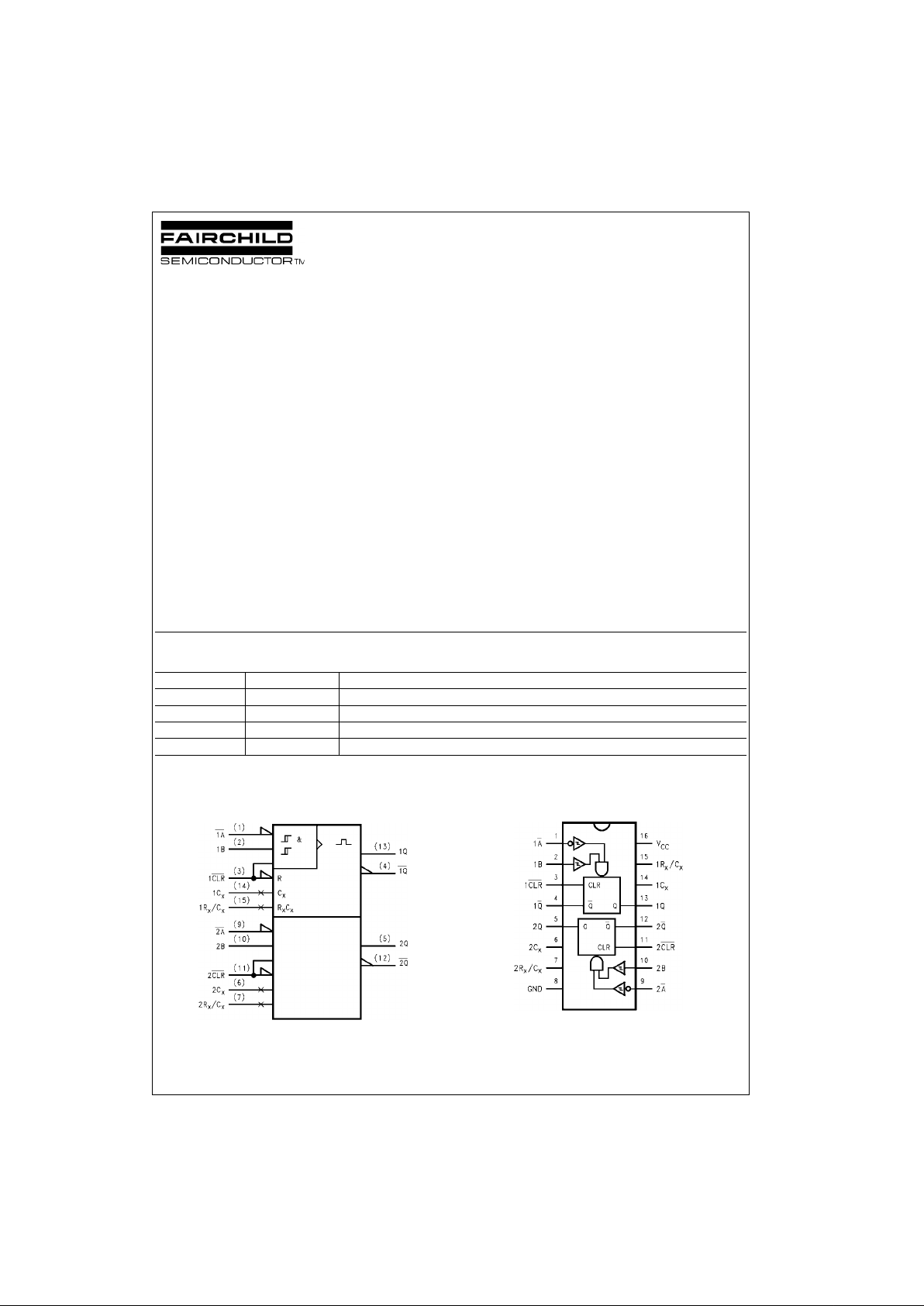
Logic Symbol
IEEE/IEC
Connection Diagram
Order Number Package Number Package Description
74VHC123AM M16A 16-Lead Small Outline Integrated Circuit (SOIC), JEDEC MS-012, 0.150” Narrow
74VHC123ASJ M16D 16-Lead Small Outline Package (SOP), EIAJ TYPE II, 5.3mm Wide
74VHC123AMTC MTC16 16-Lead Thin Shrink Small Outline Package (TSSOP), JEDEC MO-153, 4.4mm Wide
74VHC123AN N16E 16-Lead Plastic Dual-In-Line Package (PDIP), JEDEC MS-001, 0.300” Wide
Page 2
www.fairchildsemi.com 2
74VHC123A
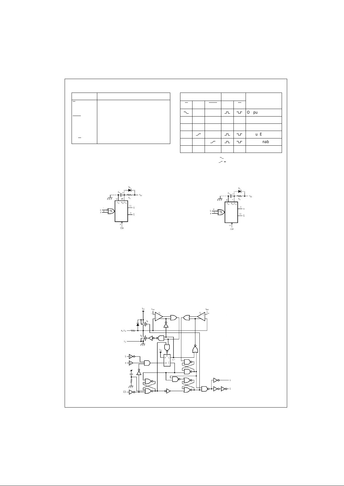
Pin Descriptions Tr uth Table
H = HIGH Voltage Level
= HIGH-to-LOW Tran s iti on
L = LOW Voltage Level
= LOW-to-HIGH Transition
X = Don’t Care
Block Diagrams
Note A: Cx, Rx, Dx are external Capaci to r, Resisto r, and Diode, res pectively.
Note B: External clamping diode, D
x
;
External capacitor is charged to V
CC
level in the wait state, i.e. w hen no trigger is applied.
If the supply voltage is turned off, C
x
discharges mainl y through the int ernal (p arasit ic) diod e. If Cx is sufficiently large a nd VCC drops rapidly, there will be
some possibility o f damag in g the IC throu gh in rus h cu rrent or latch- up . If the ca pac itance of the supp ly volt age fi lter is larg e enough and V
CC
drops slowly,
the in rush current is automatically limite d and damage to the IC is av oided.
The maximum va lue of fo rwar d c urren t t hroug h the par asit ic diode i s ±20 mA. In the case of a large Cx, the limit of fall time of the supply voltage is determined as follows:
t
f
≥ (VCC −0.7) Cx/20 mA
(t
f
is the time between the supply voltage turn off and the supply voltage reaching 0.4 VCC)
In the event a system does not satisfy the above condition, an external clamping diode (D
x
) is needed to protect the IC from rush current.
System Diagram
Pin Names Description
A
Trigger Inputs (Negative Edge)
B Trigger Inputs (Positive Edge)
CLR
Reset Inputs
C
x
External Capacitor
R
x
External Resistor
Q, Q
Outputs
Inputs Outputs Function
A
BCLRQQ
HH
Output Enable
X L H L H Inhibit
H X H L H Inhibit
L
H
Output Enable
LH
Output Enable
XX L LHReset
Page 3
3 www.fairchildsemi.com
74VHC123A
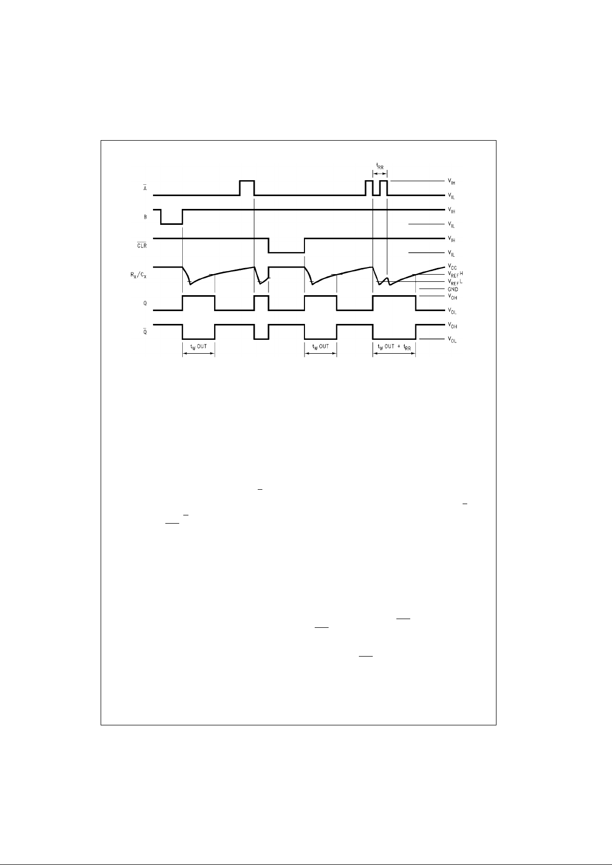
Timing Chart
Functional Description
1. Stand-by State
The external capaci tor (C
x
) is fully charged to V
CC
in
the Stand-by State. That mean s, before trigger ing, the
Q
P
and QN transistors which are connecte d to the Rx/
C
x
node are in the off state. Two comparators that
relate to the timing of the output p ulse, and two r eference voltage supplies turn off. The total supply curre nt
is only leakage current.
2. Trigger Operation
Trigger operation is effective in any of the following
three cases. First, the co ndition where the A
input is
LOW, and B input has a rising signal; second, where
the B input is HIGH, and the A input has a falling signal;
and third, where the A
input is LOW and the B input is
HIGH, and the CLR
input has a rising signal.
After a trigger becomes effecti ve, comparat ors C
1
and
C
2
start operating, and QN is turned on. The external
capacitor discharges thro ugh Q
N
. The voltage level at
the R
x/Cx
node drops. If the Rx/Cx voltage level falls to
the internal referen ce voltage V
ref
L, the output of C
1
becomes LOW. The flip-flop is then reset an d QN turns
off. At that moment C
1
stops but C2 continues operating.
After Q
N
turns off, the voltage at the Rx/Cx node starts
rising at a rate determined by the time constant of
external capacitor C
x
and resistor Rx.
Upon triggering, output Q becomes HIGH, following
some delay time of th e internal F/F and gates. It s tays
HIGH even if the voltage of R
x/Cx
changes from falling
to rising. When R
x/Cx
reaches the internal reference
voltage V
ref
H, the output of C2 becomes LOW, the out-
put Q goes LOW and C
2
stops its operation. That
means, after trigger ing, when the voltage level of the
R
x/Cx
node reaches V
ref
H, the IC returns to its
MONOSTABLE stat e.
With large values of C
x
and Rx, and ignoring the dis-
charge time of the capacitor a nd internal dela ys of the
IC, the width of the outp ut pulse, t
W
(OUT), is as follows:
t
W
(OUT) = 1.0 Cx R
x
3. Retrigger operation (74 V HC12 3A )
When a new trigger is applied to either inpu t A
or B
while in the MONOSTABLE state, it is effective only if
the IC is chargi ng C
x
. The voltage level of the Rx/C
x
node then falls to V
ref
L level again. Therefo re the Q
output stays HIGH if the next tr igger comes in before
the time period set by C
x
and Rx.
If the new trigger is very close to a previous trigger,
such as an occurrence during th e discharge cycle, it
will have no effect.
The minimum time for a tr igge r to be effecti ve 2nd trigger, t
RR
(Min), depends on VCC and Cx.
4. Reset Operation
In normal operation, the CLR
input is held HIGH. If
CLR
is LOW, a trigger has no affect because the Q output is held LOW and the tri gger control F/F is reset.
Also, Q
p
turns on and Cx is charged rapidly to VCC.
This means if CLR
is set LOW, the IC goes into a wait
state.
Page 4

www.fairchildsemi.com 4
74VHC123A
Absolute Maximum Ratings(Note 1) Recommended Operating
Conditions
(Note 2)
Note 1: Absolute maximum ratings are values beyond which the device
may be damaged or ha ve its useful li fe impaire d. The datab ook specifications should be met, without exception, to ensure that the system design is
reliable over its p ower supp ly, temperature, and ou tput/input loading variables. Fairchild do es not recommended operation outside data book specifications.
Note 2: Unused inputs must be held HIGH or LOW. They may not float.
Note 3: The maximum allowable values of C
x
and Rx are a function o f the
leakage of capacitor C
x
, the leakage of the device, and leakage due to
board layout and su rface resistance. Suscep tibility to externally induc ed
noise signals may oc c ur f or R
x
> 1MΩ.
DC Electrical Characteristics
Note 4: Per Circuit
Supply Voltage (VCC) −0.5V to +7.0V
DC Input Voltage (V
IN
) −0.5V to +7.0V
DC Output Voltage (V
OUT
) −0.5 to VCC +0.5V
Input Diode Current (I
IK
) −20 mA
Output Diode Current (I
OK
) ±20 mA
DC Output Current (I
OUT
) ±25 mA
DC V
CC
/Current (ICC) ±50 mA
Storage Temperature (T
STG
) −65°C to 150°C
Lead Temperature (T
L
)
Solderin g, 10 seconds 260°C
Supply Voltage (V
CC
) 2.0V to +5.5V
Input Voltage (V
IN
)0V to +5.5V
Output Voltage (V
OUT
) 0V to V
CC
Operating Temperature
(T
opr
) −40° to +85°C
Input Rise and Fall Time (t
r
, tf)
(CLR
only)
V
CC
= 3.3V ± 0.3V 0 ∼ 100 ns/V
V
CC
= 5.0V ± 0.5V 0 ∼ 20 ns/V
External Capacitor - C
x
No Limitation (Note 3) F
External Resistor - R
x
>5 kΩ (Note 3) (VCC = 2.0V)
>1 kΩ (Note 3) (V
CC
> 3.0V)
Symbol Parameter
V
CC
(V)
TA = 25°CT
A
= −40° to 85°C
Units Conditions
Min Typ Max Min Max
V
IH
HIGH Level 2.0 1.50 1.50
V
Input Voltage 3.0 − 5.5 0.7 V
CC
0.7 V
CC
V
IL
LOW Level 2.0 0.50 0.50
V
Input Voltage 3.0 − 5.5 0.3 V
CC
0.3 V
CC
V
OH
HIGH Level 2.0 1.9 2.0 1.9 VIN = VIHIOH = −50 µA
Output Voltage 3.0 2.9 3.0 2.9 V or V
IL
4.5 4.4 4.5 4.4
3.0 2.58 2.48
V
IOH = −4 mA
4.5 3.94 3.80 IOH = −8 mA
V
OL
LOW Level 2.0 0.0 0.1 0.1
V
VIN = VIHIOL = 50 µA
Output Voltage 3.0 0.0 0.1 0.1 or V
IL
4.5 0.0 0.1 0.1
3.0 0.36 0.44 IOL = 4 mA
4.5 0.36 0.44 IOL = 8 mA
I
IN
Input Leakage Current 0 − 5.5 ±0.1 ±1.0 µAVIN = 5.5V or GND
I
IN
Rx/Cx Terminal 5.5 ±0.25 ±2.50 µAVIN = VCC or GND
Off-State Current
I
CC
Quiescent Supply Current 5.5 4.0 40.0 µAVIN = VCC or GND
I
CC
Active—State 3.0 160 250 280 VIN = VCC or GND
(Note 4) 4.5 380 500 650 µARx/Cx = 0.5 V
CC
Supply Current 5.5 560 750 975
Page 5

5 www.fairchildsemi.com
74VHC123A
AC Electrical Characteristics (Note 5)
Note 5: Refer to Timing Char t.
Note 6: C
PD
is defined as the value of the internal equi v alent capacitance w hic h is calculated from t he operating curre nt c ons umption without load. Av erage
operating current ca n be obtained by the equ at ion:
I
CC
(opr.) = CPD*VCC*f
IN+ ICC
1
*Duty/100 + ICC/2 (per Circuit)
I
CC
1
: Active Supply Current
Duty:%
AC Operating Requirement (Note 7)
Note 7: Refer to Timing Char t.
Symbol Parameter
V
CC
(V)
TA = 25°CT
A
= −40°C to +85°C
Units Conditions
Min Typ Max Min Max
t
PLH
t
PHL
Propagation Delay Time 3.3 ± 0.3 13.4 20.6 1.0 24.0
ns
CL = 15 pF
(A, B–Q, Q)
15.9 24.1 1.0 27.5 CL = 50 pF
5.0 ± 0.5 8.1 12.0 1.0 14.0
ns
CL = 15 pF
9.6 14.0 1.0 16.0 CL = 50 pF
t
PLH
t
PHL
Propagation Delay Time 3.3 ± 0.3 14.5 22.4 1.0 26.0
ns
CL = 15 pF
(CLR Trigger—Q, Q \)
17.0 25.9 1.0 29.5 CL = 50 pF
5.0 ± 0.5 8.7 12.9 1.0 15.0
ns
CL = 15 pF
10.2 14.9 1.0 17.0 CL = 50 pF
t
PLH
t
PHL
Propagation Delay Time 3.3 ± 0.3 10.3 15.8 1.0 18.5
ns
CL = 15 pF
(CLR—Q, Q)
12.8 19.3 1.0 22.0 CL = 50 pF
5.0 ± 0.5 6.3 9.4 1.0 11.0
ns
CL = 15 pF
7.8 11.4 1.0 13.0 CL = 50 pF
t
WOUT
Output Pulse Width 3.3 ± 0.3 160 240 300
ns
CL = 50 pF Cx = 28 pF
5.0 ± 0.5 133 200 240 Rx = 2 kΩ
3.3 ± 0.3 90 100 110 90 110
µs
CL = 50 pF Cx = 0.01 µF
5.0 ± 0.5 90 100 110 90 110 Rx = 10 kΩ
3.3 ± 0.3 0.9 1.0 1.1 0.9 1.1
ms
CL = 50 pF Cx = 0.1 µF
5.0 ± 0.5 0.9 1.0 1.1 0.9 1.1 Rx = 10 kΩ
∆t
WOUT
Output Pulse Width Error
Between Circuits ±1%
(In same Package)
C
IN
Input Capacitance 4 10 10 pF VCC = Open
C
PD
Power Dissipation 73 pF (Note 6)
Capacitance
Symbol Parameter
V
CC
(V)
TA = 25°CT
A
= −40°C to +85°C
Units Conditions
Min Typ Max Min Max
tW(L) Minimum Trigger 3.3 5.0 5.0
ns
tW(H) Pulse Width 5.0 5.0 5.0
tW(L) Minimum Clear 3.3 5.0 5.0 ns
Pulse Width 5.0 5.0 5.0
t
RR
Minimum 3.3 ± 0.3 60 ns Rx = 1 kΩ
Retrigger Time 5.0 ± 0.5 39 CX = 100 pF
3.3 1.5 µsRx = 1 kΩ
5.0 1.2 CX = 0.01 µF
Page 6

www.fairchildsemi.com 6
74VHC123A
Device Characteristics
t
wout*Cx
Characteristics (ty p) tRR*VCC Characteristics (typ)
Output Pulse Width Constant K-Supply Voltage
(Typical)
Input Equivalent Circuit
Page 7

7 www.fairchildsemi.com
74VHC123A
Physical Dimensions inches (millimeters) unless otherwise noted
16-Lead Small Outline Integrated Circuit (SOIC), JEDEC MS-012, 0.150” Narrow
Package Number M16A
16-Lead Small Outline Package (SOP), EIAJ TYPE II, 5.3mm Wide
Package Number M16D
Page 8

www.fairchildsemi.com 8
74VHC123A
Physical Dimensions inches (millimeters) unless otherwise noted (Continued)
16-Lead Thin Shrink Small Outline Package (TSSOP), JEDEC MO-153, 4.4mm Wide
Package Number MTC16
Page 9

Fairchild does not assume any responsibility for use of any circuitry described, no circuit patent licenses are implied and Fairchild reserves the right at any time without notice to change said circuitry and specifications.
74VHC123A Dual Retriggerable Monostable Multivibrator
LIFE SUPPORT POLICY
FAIRCHILD’S PRODUCTS ARE NOT AUTHORIZED FOR USE AS CRITICAL COMPONENTS IN LIFE SUPPORT
DEVICES OR SYSTEMS WITHOUT THE EXPRESS WRITTEN APPROVAL OF THE PRESIDENT OF FAIRCHILD
SEMICONDUCTOR CORPORATION. As used herein:
1. Life sup port de vices o r syst ems are devices or systems
which, (a) are intended for surgical implant into the
body, or (b) support or sustain life, and (c) whose failure
to perform when properly used in accordance with
instructions for use provided i n the labe li ng, can be re asonably expected to result in a significant injury to the
user.
2. A cri tical componen t in any com ponen t of a life s upport
device or system whose failu re to perform can b e reasonably expected to c ause th e fa i lure of the li fe s upp or t
device or system, or to affect its safety or effectiveness.
www.fairchildsemi.com
Physical Dimensions inches (millimeters) unless otherwise noted (Continued)
16-Lead Plastic Dual-In-Line Package (PDIP), JEDEC MS-001, 0.300” Wide
Package Number N16E
 Loading...