

Page 1
QUAD 2-INPUT OPEN DRAIN NAND GATE
■ HIGHSPEED:t
■ LOW POWER DISSIPATION:
=2 µA (MAX.)at TA=25oC
I
CC
■ HIGHNOISEIMMUNITY:
V
NIH=VNIL
■ POWERDOWNPROTECTIONON INPUTS
■ OPERATINGVOLTAGERANGE:
V
CC
■ PINANDFUNCTIONCOMPATIBLEWITH
=28%VCC(MIN.)
(OPR)= 2Vto5.5V
74SERIES03
■ IMPROVEDLATCH-UPIMMUNITY
■ LOWNOISE:V
DESCRIPTION
The 74VHC03 is an advanced high-speedCMOS
QUAD 2-INPUT OPEN DRAIN NAND GATE
fabricated with sub-micron silicon gate and
double-layermetal wiring C
The internal circuit is composed of 3 stages
including buffer output, which provides high noise
immunityand stableoutput.
This device can, with an external pull-up resistor,
=3.7ns(TYP.)atVCC=5V
PD
= 0.8V(Max.)
OLP
2
MOS technology.
74VHC03
PRELIMINARY DATA
M
(Micro Package)
(TSSOPPackage)
ORDERCODES :
74VHC03M 74VHC03T
be used in wired AND configuration. This device
can also be used as a led driver and in anyother
applicationrequiring a currentsink.
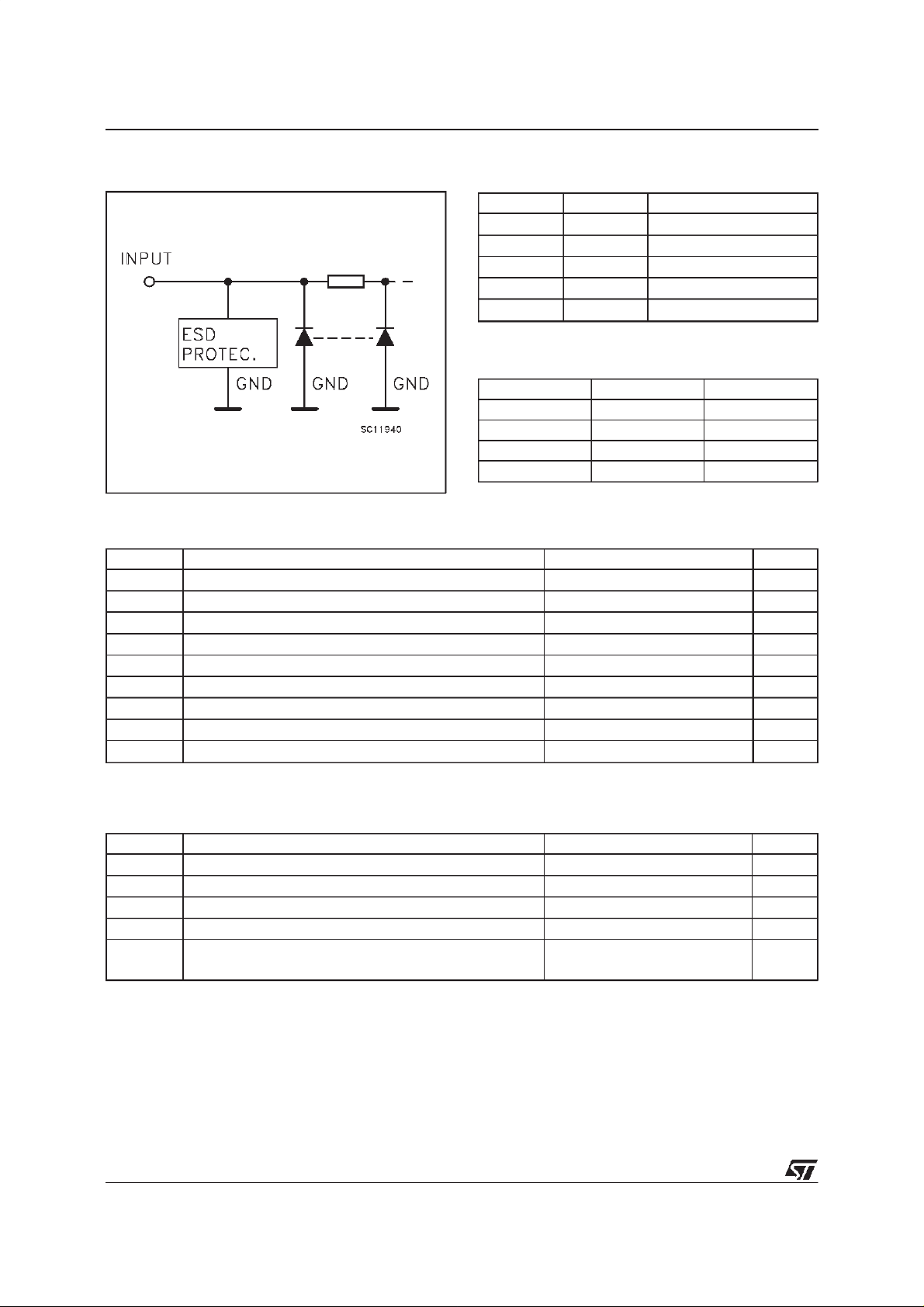
Power down protection is provided on all inputs
and 0 to 7V can be accepted on inputs with no
regard to the supply voltage. This device can be
used to interface 5V to 3V.
All inputs and outputs are equipped with
protection circuits against static discharge, giving
them 2kV ESD immunity and transient excess
voltage.
T
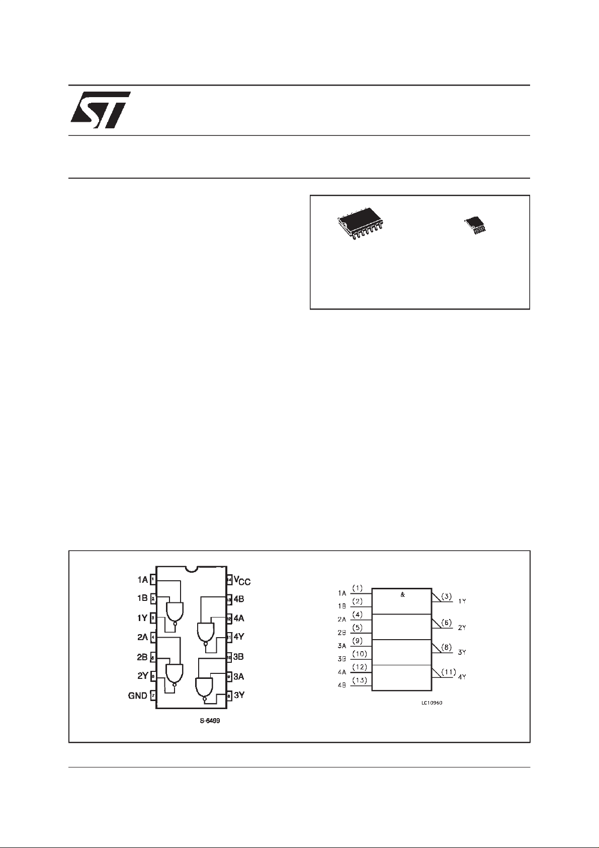
PIN CONNECTION AND IEC LOGICSYMBOLS
June 1999
1/7
Page 2
74VHC03
INPUT EQUIVALENTCIRCUIT
PIN DESCRIPTION
PI N No SYMB OL NAME AND FU NCTIO N
1, 4, 9, 12 1A to 4A Data Inputs
2, 5, 10,13 1B to 4B Data Inputs
3, 6, 8, 11 1Y to 4Y Data Outputs
7 GND Ground (0V)
14 V
CC
Positive Supply Voltage
TRUTH TABLE
ABY
LLZ
LHZ
HLZ
HHL
Z: High Impedance
ABSOLUTE MAXIMUM RATINGS
Symb o l Para met er Val u e Uni t
V
V
V
I
I
OK
I
or I
I
CC
T
T
AbsoluteMaximumRatingsarethosevaluesbeyondwhichdamageto thedevicemayoccur.Functionaloperation underthesecondition isnotimplied.
Supply Voltage -0.5 to +7.0 V
CC
DC Input Voltage -0.5 to +7.0 V
I
DC Output Voltage -0.5 to VCC+ 0.5 V
O
DC Input Diode Current - 20 mA
IK
DC Output Diode Current ± 20 mA
DC Output Current 25 mA
O
DC VCCor Ground Current ± 50 mA
GND
Storage Temperature -65 to +150
stg
Lead Temperature (10 sec) 300
L
o
C
o
C
RECOMMENDED OPERATINGCONDITIONS
Symb o l Para met er Value Un it
V
V
V
T
dt/dv
1)VINfrom30%to70%of V
2/7
Supply Voltage 2.0 to 5.5 V
CC
Input Voltage 0 to 5.5 V
I
Output Voltage 0 to V
O
Operating Temperature -40 to +85
op
(V
CC
CC
=3.3±0.3V)
=5.0±0.5V)
Input Rise and Fall Time (see note 1) (V
CC
CC
0 to 100
0to20
V
o
C
ns/V
ns/V
Page 3
74VHC03
DC SPECIFICATIONS
Symb o l Para met er Test C o n diti o ns Val u e Uni t
T
V
CC
(V)
High Level Input
V
IH
Voltage
V
Low Level Input
IL
Voltage
V
Low Level Output
OL
Voltage
2.0 1.5 1.5
3.0 to 5.5 0.7V
2.0 0.5 0.5
3.0 to 5.5 0.3V
2.0 IO=50 µ A 0.0 0.1 0.1
3.0 I
4.5 I
3.0 I
4.5 I
High Impedance
I
OZ
Output Leakage
5.5
VO=VCCor GND
Current
Input Leakage Current 0 to 5.5 VI= 5.5V or GND
I
I
Quiescent Supply
I
CC
5.5 VI=VCCorGND 2 20
Current
Min. Typ. Max. Min. Max.
=50µA 0.0 0.1 0.1
O
=50µA 0.0 0.1 0.1
O
=4 mA 0.36 0.44
O
=8 mA 0.36 0.44
O
VI=VIHor V
IL
=25oC -40 to 85oC
A
CC
0.7V
CC
±0.25 ±2.5 µA
0.1
±
CC
0.3V
±
1.0
CC
µ
µ
V
V
V
A
A
AC ELECTRICAL CHARACTERISTICS (Inputtr=tf=3ns)
Symbol Parameter T est Condition Value Unit
t
Propagation Delay
PZL
Time
t
Propagation Delay
PLZ
Time
(*) Voltagerange is3.3V± 0.3V
(**) Voltagerangeis 5V± 0.5V
V
(V)
3.3
3.3
5.0
5.0
3.3
5.0
CC
(**)
(**)
(**)
C
L
(pF)
(*)
(*)
15 RL=1KΩ 5.5 7.9 1.0 9.5
50 RL=1KΩ 8.0 11.4 1.0 13.0
15 RL=1K
Ω
T
=25oC -40 to 85oC
A
Mi n . Typ. Max. Mi n . Max.
3.7 5.5 1.0 6.5
ns
50 RL=1KΩ 5.2 7.5 1.0 8.5
(*)
50 RL=1K
Ω
8.0 11.4 1.0 13.0
50 RL=1KΩ 5.2 7.5 1.0 8.5
ns
CAPACITIVE CHARACTERISTICS
Symb o l Para met er Test C o n diti o ns Val u e Uni t
=25oC -40 to 85oC
T
A
Min. Typ. Max. Min. Max.
Input Capacitance 4 10 10
C
IN
C
Output Capacitance 5
OUT
Power Dissipation
C
PD
6pF
Capacitance (note 1)
1)CPDisdefined asthevalue oftheIC’sinternal equivalentcapacitance whichis calculated fromtheoperatingcurrent consumptionwithout load.(Referto
TestCircuit).Average operatingcurrent canbeobtainedbythefollowingequation.I
(opr)= CPD• VCC• fIN+ICC/4(perGate)
CC
pF
pF
3/7
Page 4

74VHC03
DYNAMICSWITCHING CHARACTERISTICS
Symb o l Para met er Test C o n diti o ns Val u e Uni t
T
V
CC
(V)
V
V
V
Dynamic Low Voltage
OLP
Quiet Output (note 1, 2)
OLV
Dynamic High Voltage
IHD
5.0
5.0 3.5
C
L
=50pF
Min. Typ. Max. Min. Max.
Input (note 1, 3)
V
Dynamic Low Voltage
ILD
5.0 1.5
Input (note 1, 3)
1)Worstcasepackage.
2)Maxnumberofoutputsdefined as(n).Datainputs aredriven 0Vto5.0V,(n -1)outputsswitching andoneoutputatGND.
3)Maxnumberofdatainputs (n)switching. (n-1)switching0V to5.0V.Inputsundertestswitching: 5.0Vtothreshold(V
TESTCIRCUIT
=25oC -40 to 85oC
A
0.3 0.8
-0.8 -0.3
),0Vtothreshold(V
ILD
),f=1MHz.
IHD
V
CL= 15/50 pF orequ ivalent (includes jigand probe capacitance)
R
=1KΩ orequivalent
L=R1
R
ofpulse generator (typically50Ω)
T=ZOUT
WAVEFORM:PROPAGATIONDELAYS
4/7
(f=1MHz;50% duty cycle)
Page 5

SO-14 MECHANICALDATA
74VHC03
DIM.
MIN. TYP. MAX. MIN. TYP. MAX.
A 1.75 0.068
a1 0.1 0.2 0.003 0.007
a2 1.65 0.064
b 0.35 0.46 0.013 0.018
b1 0.19 0.25 0.007 0.010
C 0.5 0.019
c1 45 (typ.)
D 8.55 8.75 0.336 0.344
E 5.8 6.2 0.228 0.244
e 1.27 0.050
e3 7.62 0.300
F 3.8 4.0 0.149 0.157
G 4.6 5.3 0.181 0.208
L 0.5 1.27 0.019 0.050
M 0.68 0.026
S 8 (max.)
mm inch
P013G
5/7
Page 6

74VHC03
TSSOP14 MECHANICAL DATA
DIM.
mm inch
MIN. TYP. MAX. MIN. TYP. MAX.
A 1.1 0.433
A1 0.05 0.10 0.15 0.002 0.004 0.006
A2 0.85 0.9 0.95 0.335 0.354 0.374
b 0.19 0.30 0.0075 0.0118
c 0.09 0.20 0.0035 0.0079
D 4.9 5 5.1 0.193 0.197 0.201
E 6.25 6.4 6.5 0.246 0.252 0.256
E1 4.3 4.4 4.48 0.169 0.173 0.176
e 0.65 BSC 0.0256BSC
K0
o
o
4
o
8
o
0
o
4
L 0.50 0.60 0.70 0.020 0.024 0.028
o
8
A
PIN 1 IDENTIFICATION
6/7
A2
A1
b
e
c
K
L
E
D
E1
1
Page 7

74VHC03
Information furnished is believed to beaccurate and reliable. However, STMicroelectronics assumes no responsibility forthe consequences
of use of such information nor for any infringement of patents or other rights of third parties which may result from its use. No license is
granted by implication or otherwise under any patent or patent rights of STMicroelectronics. Specification mentioned in this publication are
subject tochange without notice. Thispublication supersedes and replaces all information previously supplied. STMicroelectronics products
are not authorized for use as critical components in life support devices or systems without express written approval of STMicroelectronics.
The ST logo is a trademark of STMicroelectronics
1999 STMicroelectronics – Printed in Italy –All Rights Reserved
STMicroelectronics GROUP OF COMPANIES
Australia - Brazil - Canada - China -France -Germany - Italy - Japan - Korea - Malaysia - Malta - Mexico -Morocco - The Netherlands -
Singapore - Spain -Sweden - Switzerland- Taiwan - Thailand - UnitedKingdom -U.S.A.
http://www.st.com
.
7/7
 Loading...