

Page 1
1/11February 2003
■ 3.6V TOLERANT INPUTS AND OUTPUTS
■ HIGH SPEED :
t
PD
= 2.5 ns (MAX.) at VCC=3.0to3.6V
t
PD
= 3.0 ns (MAX.) at VCC=2.3to2.7V
■ POWER DOWN PROTECTION ON INPUTS
AND OUTPUTS
■ SYMMETRICAL OUTPUT IMPEDANCE:
|I
OH
|=IOL= 24mA (MIN) at VCC=3.0V
|I
OH
|=IOL= 18mA (MIN) at VCC=2.3V
■ OPERATING VOLTAGE RANGE:
V
CC
(OPR) = 2.3V to 3.6V
■ PIN AND FUNCTION COMPATIBLE WITH
74 SERIES H16240
■ BUS HOLD PROVIDED ON DATA INPUTS
■ LATCH-UP P ERFO RMANCE EXCEEDS
300mA (JESD 17)
■ ESD PERFORMANCE:
HBM > 2000V (MIL STD 883 method 3015);
MM > 200V
DESCRIPTION
The 74VCXH16240 is a low voltage CMOS 16 BIT
BUS BUFFER (INVERTED) fabricated with
sub-micron silicon gate and five-layer metal wiring
C
2
MOS technology. It is ideal for low power and
very high s peed 2.3 to 3.6V applications; it can be
interfaced to 3.6V signal environment for both
inputs and outputs.
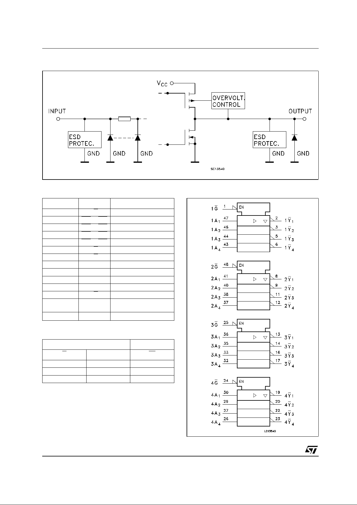
Any nG
output con trol governs four BUS
BUFFERS. Output Enable input (nG
) tied together
gives full 16-bit operation.
When nG
is LO W, the outputs are on. When nG is
HIGH, the output are in high impedance state.
This dev ice is designed to be us ed with 3 state
memory address drivers, etc. Bus hold on data
inputs is p ro vided in order to eli minate the need f or
external pull-up or pull-down resistor.
All inputs and outputs are equipped with
protection circuits against static discharge, giving
them 2KV ESD imm unity and transient excess
voltage.
74VCXH16240
LOW VOLTAGE CMOS 16-BIT BUS BUFFER (3-STATE INV.)
WITH 3.6V TOLERANT INPUTS AND OUTPUTS
ORDER CODES
PACKAGE TUBE T & R
TSSOP 74VCXH16240TTR
TSSOP
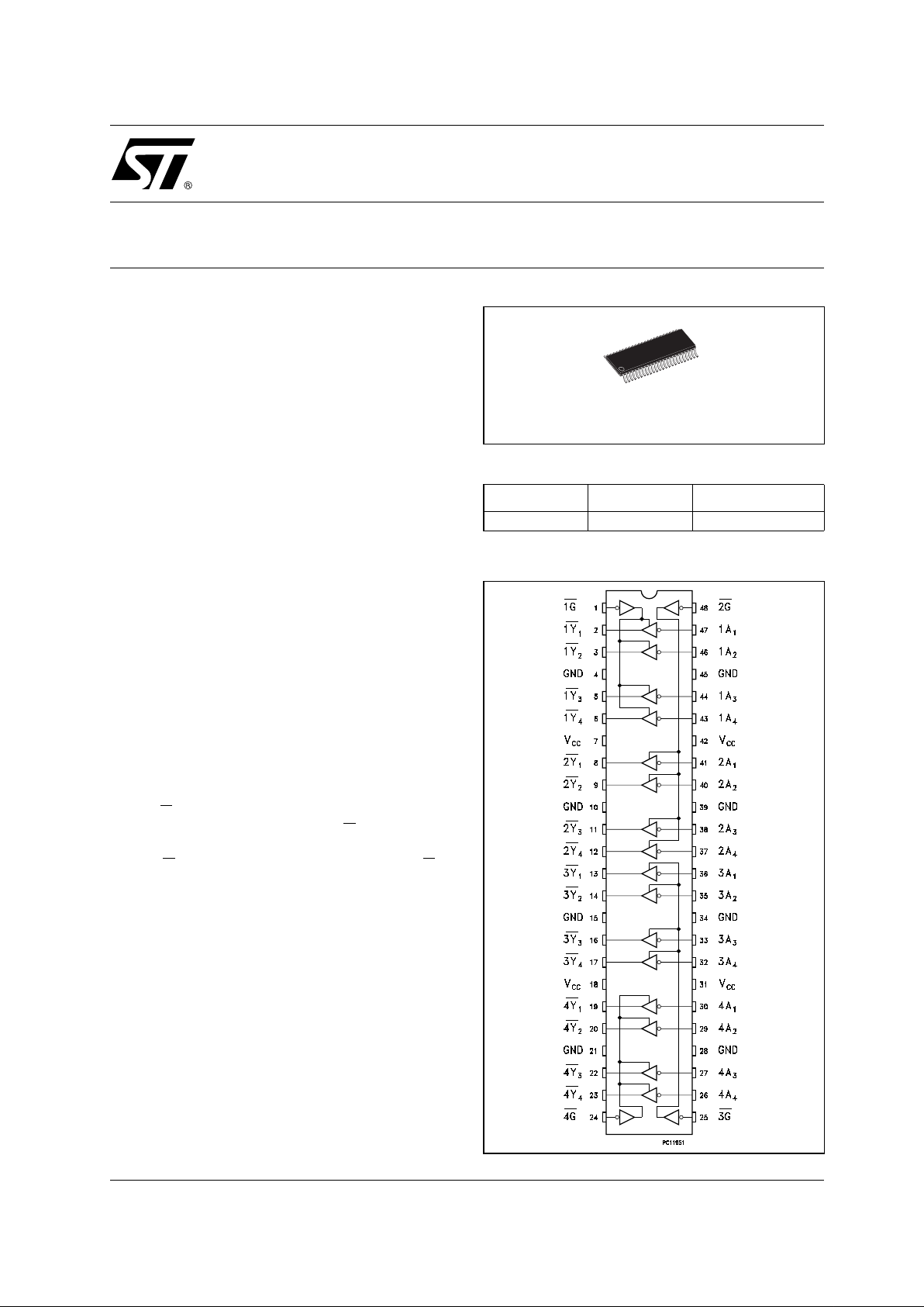
PIN CO NNE CTION
Page 2
74VCXH16240
2/11
INPUT AND OUTPUT EQUIVALENT CIRCUIT
PIN DESCRIPTION
TRUTH TABLE
X : Don‘t Care
Z : High Impedance
IEC LOGIC SYMBOLS
PIN No SYMBOL NAME AND FUNCTION
11G
Output Enable Input
2, 3, 5, 6 1Y1
to 1Y4 Data Outputs
8, 9, 11, 12 2Y1
to 2Y4 Data Outputs
13, 14, 16, 17 3Y1
to 3Y4 Data Outputs
19, 20, 22, 23 4Y1
to 4Y4 Data Outputs
24 4G
Output Enable Input
25 3G
Output Enable Input
30, 29, 27, 26 4A1 to 4A4 Data Outputs
36, 35, 33, 32 3A1 to 3A4 Data Outputs
41, 40, 38, 37 2A1 to 2A4 Data Outputs
47, 46, 44, 43 1A1 to 1A4 Data Outputs
48 2G
Output Enable Input
4, 10, 15, 21,
28, 34, 39, 45
GND Ground (0V)
7, 18, 31, 42
V
CC
Positive Supply Voltage
INPUTS OUTPUT
G
An Yn
LLH
LHL
HXZ
Page 3
74VCXH16240
3/11
ABSOLUTE MAXIMUM RATINGS
Absolute Maximum Ratings are those values beyond which damage to the device may occur. Functional operation under these conditions is
not implied
1) I
O
absolute maximum rating must be observed
2) V
O
<GND,VO>V
CC
RECOMMENDED OPERATING CONDITIONS
1) VINfrom0.8Vto 2V at VCC=3.0V
Symbol Parameter Value Unit
V
CC
Supply Voltage
-0.5 to +4.6 V
V
I
DC Input Voltage
-0.5 to +4.6 V
V
O
DC Output Voltage (OFF State)
-0.5 to +4.6 V
V
O
DC Output Voltage (High or Low State) (note 1) -0.5 to VCC+ 0.5
V
I
IK
DC Input Diode Current
-50 mA
I
OK
DC Output Diode Current (note 2)
-50 mA
I
O
DC Output Current
± 50 mA
I
CC
or I
GND
DC VCCor Ground Current per Supply Pin
± 100 mA
P
D
Power Dissipation
400 mW
T
stg
Storage Temperature
-65 to +150 °C
T
L
Lead Temperature (10 sec)
300 °C
Symbol Parameter Value Unit
V
CC
Supply Voltage
2.3 to 3.6 V
V
I
Input Voltage
-0.3 to 3.6 V
V
O
Output Voltage (OFF State)
0 to 3.6 V
V
O
Output Voltage (High or Low State) 0 to V
CC
V
I
OH,IOL
High or Low Level Output Current (VCC= 3.0 to 3.6V)
± 24 mA
I
OH,IOL
High or Low Level Output Current (VCC= 2.3 to 2.7V)
± 18 mA
T
op
Operating Temperature
-55 to 125 °C
dt/dv Input Rise and Fall Time (note 1) 0 to 10 ns/V
Page 4
74VCXH16240
4/11
DC SPECIFICATIONS (2.7V < VCC< 3.6V unless otherwise specified)
Symbol Parameter
Test Condition Value
Unit
V
CC
(V)
-40to85°C -55to125°C
Min. Max. Min. Max.
V
IH
High Level Input
Voltage
2.7to3.6
2.0 2.0
V
V
IL
Low Level Input
Voltage
0.8 0.8
V
OH
High Level Output
Voltage
2.7to3.6
IO=-100 µAVCC-0.2 VCC-0.2
V
2.7
I
O
=-12 mA
2.2 2.2
3.0
I
O
=-18 mA
2.4 2.4
I
O
=-24 mA
2.2 2.2
V
OL
Low Level Output
Voltage
2.7to3.6
IO=100 µA
0.2 0.2
V
2.7
I
O
=12 mA
0.4 0.4
3.0
I
O
=18 mA
0.4 0.4
I
O
=24 mA
0.55 0.55
I
I
Input Leakage
Current
2.7to3.6
V
I=VCC
or GND
± 5 ± 5 µA
I
I(HOLD)
Input Hold Current
3.0
VI= 0.8V
75 75
µA
V
I
=2V
-75 -75
3.6
V
I
= 0 to 3.6V
± 500 ± 500
I
off
Power Off Leakage
Current
0
V
I
or VO= 0 to 3.6V
10 10 µA
I
OZ
High Impedance
Output Leakage
Current
2.7to3.6
V
I=VIH
or V
IL
VO= 0 to 3.6V
± 10 ± 10 µA
I
CC
Quiescent Supply
Current
2.7to3.6
V
I=VCC
or GND
20 20
µA
V
I
or VO=VCCto
3.6V
± 20 ± 20
∆I
CC
ICCincr. per Input
2.7to3.6
VIH=VCC-0.6V
750 750 µA
Page 5

74VCXH16240
5/11
DC SPECIFICATIONS (2.3V < VCC< 2.7V unless otherwise specified)
DYNAMIC SWITCHING CHARA CTERISTICS (T
a
= 25°C, Input tr=tf= 2.0ns, CL= 30pF, RL= 500Ω)
1) Number of outputsdefined as "n". Measured with"n-1"outputs switchingfromHIGH to LOW or LOW to HIGH. The remaining outputis
measured in the LOW state.
2) Number of outputsdefined as "n". Measured with"n-1"outputs switchingfromHIGH to LOW or LOW to HIGH. The remaining outputis
measured in the HIGH state.
3) Parameters guaranteed by design.
Symbol Parameter
Test Condition Value
Unit
V
CC
(V)
-40to85°C -55to125°C
Min. Max. Min. Max.
V
IH
High Level Input
Voltage
2.3to2.7
1.6 1.6
V
V
IL
Low Level Input
Voltage
0.7 0.7
V
OH
High Level Output
Voltage
2.3to2.7
IO=-100 µAVCC-0.2 VCC-0.2
V
2.3
I
O
=-6 mA
2.0 2.0
I
O
=-12 mA
1.8 1.8
I
O
=-18 mA
1.7 1.7
V
OL
Low Level Output
Voltage
2.3to2.7
IO=100 µA
0.2 0.2
V
2.3
I
O
=12 mA
0.4 0.4
I
O
=18 mA
0.6 0.6
I
I
Input Leakage
Current
2.3to2.7
V
I=VCC
or GND
± 5 ± 5 µA
I
I(HOLD)
Input Hold Current
2.3
VI= 0.7V
45 45
µA
V
I
= 1.7V
-45 -45
I
off
Power Off Leakage
Current
0
V
I
or VO= 0 to 3.6V
10 10 µA
I
OZ
High Impedance
Output Leakage
Current
2.3to2.7
V
I=VIH
or V
IL
VO= 0 to 3.6V
± 10 ± 10 µA
I
CC
Quiescent Supply
Current
2.3to2.7
VI=VCCor GND
20 20
µA
V
I
or VO=VCCto
3.6V
± 20 ± 20
Symbol Parameter
Test Condition Value
Unit
V
CC
(V)
T
A
=25°C
Min. Typ. Max.
V
OLP
Dynamic Low Voltage Quiet
Output (note 1, 3)
2.5 VIL=0V
V
IH=VCC
0.6
V
3.3 0.8
V
OLV
Dynamic Low Voltage Quiet
Output (note 1, 3)
2.5 VIL=0V
V
IH=VCC
-0.6
V
3.3 -0.8
V
OHV
Dynamic High Voltage Quiet
Output (note 2, 3)
2.5 VIL=0V
V
IH=VCC
1.9
V
3.3 2.2
Page 6

74VCXH16240
6/11
AC ELECTRICAL C HARACTERISTICS (CL= 30pF, RL= 500Ω, Input tr=tf= 2.0ns)
1) Skew is defined as the absolute value of the difference between the actual propagation delay for any two outputs of the same device switching in the same direction, either HIGH or LOW (t
OSLH
=|t
PLHm-tPLHn
|, t
OSHL
=|t
PHLm-tPHLn
|)
2) Parameter guaranteed by design
CAPACITIVE CHARACTERISTICS
1) CPDis defined as the value of the IC’s internal equivalent capacitance which is calculated from the operating current consumption without
load. (Refer to Test Circuit). Average operating current can be obtained by the following equation. I
CC(opr)=CPDxVCCxfIN+ICC
/16 (per
circuit)
Symbol Parameter
Test Condition Value
Unit
V
CC
(V)
-40 to 85 °C -55 to 125 °C
Min. Max. Min. Max.
t
PLHtPHL
Propagation Delay
Time
2.3 to 2.7 1.0 3.0 1.0 3.8
ns
3.0 to 3.6 0.8 2.5 0.8 3.3
t
PZLtPZH
Output Enable Time 2.3 to 2.7 1.0 4.1 1.0 4.6
ns
3.0 to 3.6 0.8 3.5 0.8 4.1
t
PLZtPHZ
Output Disable Time 2.3 to 2.7 1.0 3.8 1.0 4.3
ns
3.0 to 3.6 0.8 3.5 0.8 4.1
t
OSLHtOSHL
Output To Output
Skew Time (note1, 2)
2.3 to 2.7 0.5 0.5
ns
3.0 to 3.6 0.5 0.5
Symbol Parameter
Test Condition Value
Unit
V
CC
(V)
T
A
=25°C
Min. Typ. Max.
C
IN
Input Capacitance
2.5 or 3.3
VIN= 0 or V
CC
6pF
C
OUT
Output Capacitance
2.5 or 3.3
VIN= 0 or V
CC
7pF
C
PD
Power Dissipation Capacitance
(note 1)
2.5 or 3.3 fIN= 10MHz
V
IN
= 0 or V
CC
20 pF
Page 7

74VCXH16240
7/11
TEST CIRCUIT
CL= 30 pF or equivalent (includes jig and probe capacitance)
R
L
=R1=500Ω or equivalent
R
T=ZOUT
of pulse generator (typically 50Ω)
WAVEFORM SYMBOL VALUES
TEST SWITCH
t
PLH,tPHL
Open
t
PZL,tPLZ(VCC
= 3.0 to 3.6V)
6V
t
PZL,tPLZ(VCC
= 2.3 to 2.7V) 2V
CC
t
PZH,tPHZ
GND
Symbol
V
CC
3.0 to3.6V 2.3 to 2.7V
V
IH
2.7V
V
CC
V
M
1.5V
V
CC
/2
V
X
VOL+ 0.3V VOL+ 0.15V
V
Y
VOH- 0.3V VOH- 0.15V
Page 8

74VCXH16240
8/11
WAVEFORM 1: PROPAGATION DELAYS (f=1MHz; 50% duty cycle)
WAVEFORM 2: OUTPUT ENABLE AND DISABLE TIME (f=1MHz; 50% duty cycle)
Page 9

74VCXH16240
9/11
DIM.
mm. inch
MIN. TYP MAX. MIN. TYP. MAX.
A 1.2 0.047
A1 0.05 0.15 0.002 0.006
A2 0.9 0.035
b 0.17 0.27 0.0067 0.011
c 0.09 0.20 0.0035 0.0079
D 12.4 12.6 0.488 0.496
E 8.1 BSC 0.318 BSC
E1 6. 0 6.2 0.236 0.244
e 0.5 BSC 0.0197 BSC
K0˚ 8˚0˚ 8˚
L 0.50 0.75 0.020 0. 030
TSSOP48 MECHANICAL DATA
c
E
b
A2
A
E1
D
1
PIN 1 IDENTIFICATION
A1
L
K
e
7065588C
Page 10

74VCXH16240
10/11
DIM.
mm. inch
MIN. TYP MAX. MIN. TYP. MAX.
A 330 12.992
C 12.8 13.2 0.504 0.519
D 20.2 0.795
N 60 2.362
T 30.4 1.197
Ao 8.7 8.9 0.343 0.350
Bo 13.1 13.3 0.516 0.524
Ko 1.5 1.7 0.059 0.067
Po 3.9 4.1 0.153 0.161
P 11.9 12.1 0.468 0.476
Tape & Reel TSSOP48 MECHANICAL DATA
Page 11

74VCXH16240
11/11
Information furnished is believed to be accurate and reliable. However, STMicroelectronics assumes no responsibility for the
consequences of use o f suc h inf ormat ion n or f or an y infr ingeme nt of paten ts or oth er ri gh ts of third part ies whic h may resul t f rom
its use. No license is granted by implication or otherwise under any patent or patent rights of STMicroelectronics. Specifications
mentioned in this publication are subject to change without notice. This publication supersedes and replaces all information
previously supplied. STMicroelectronics products are not authorized for use as critical components in life support devices or
systems without express written approval of STMicroelectronics.
© The ST logo is a registered trademark of STMicroelectronics
© 2003 STMicroelectronics - Printed in Italy - All Rights Reserved
STMicroelectronics GROUP OF COMPANIES
Australia - Brazil - Canada - China - Finland - France - Germany - Hong Kong - India - Israel - Italy - Japan - Malaysia - Malta - Morocco
Singapore - Spain - Sweden - Switzerland - United Kingdom - United States.
© http://www.st.com
 Loading...