

Page 1
© 1999 Fairchild Semiconductor Corporation ds500163 www.fairchildsemi.com
July 1999
Revised July 1999
74VCX86 Low Voltage Quad 2-Input Exclusive-OR Gate with 3.6V Tolerant Inputs and Outputs
74VCX86
Low Voltage Quad 2-Input Exclusive-OR Gate with
3.6V Tolerant Inputs and Outputs
General Description
The VCX86 contains four 2-inp ut exclu sive OR ga tes. This
product is designed for low voltage (1.65V to 3.6V) V
CC
applications with I/O compatibility up to 3.6V
The 74VCX86 is fabr icated w ith an adva nced CM OS tec h-
nology to achieve high-speed oper ation while maintaining
low CMOS power dissipation.
Features
■ 1.65V-3.6V VCC supply operation
■ 3.6V tolerant inputs and outputs
■ t
PD
3.0 ns max for 3.0V to 3.6V V
CC
3.9 ns max for 2.3V to 2.7V V
CC
7.8 ns max for 1.65V to 1.95V V
CC
■ Power-off high impedance inputs and outputs
■ Static Drive (I
OH/IOL
)
±24 mA @ 3.0V V
CC
±18 ma @ 2.3V V
CC
±6 mA @ 1.65V V
CC
■ Uses patented Quiet Series noise/EMI reduction
circuitry
■ Latchup performance exceeds 300 mA
■ ESD performance:
Human body model > 2000V
Machine model > 250V
Ordering Code:
Devices also availab le in Tape and Reel. Specify by appending th e s uffix let t er “X” to the ordering code.
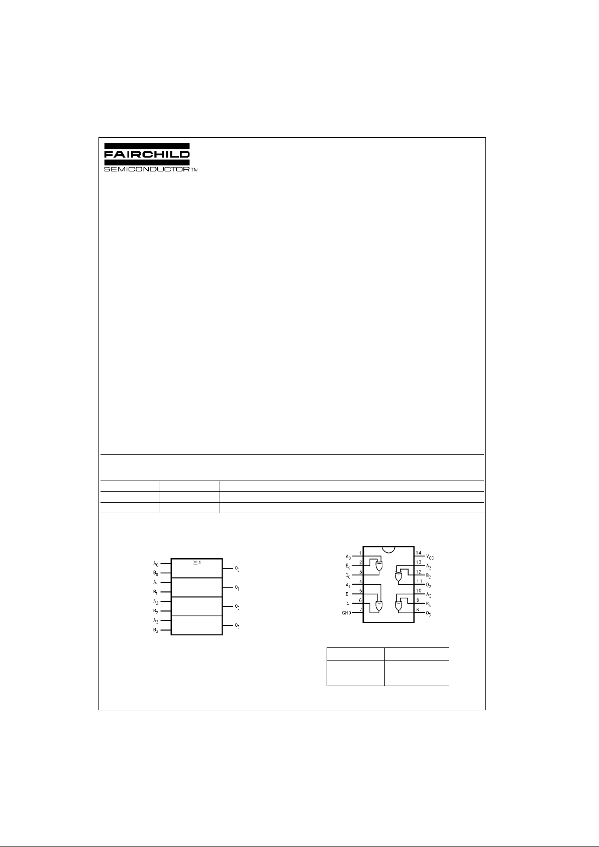
Logic Symbol
IEEE/IEC
Connection Diagram
Pin Descriptions
Quiet Series is a trademark of Fairchild Semiconductor Corporation
Order Number Package Number Package Description
74VCX86M M14A 14-Lead Small Outline Integrated Circuit (SOIC), JEDEC MS-120, 0.150” Narrow
74VCX86MTC MTC14 14-Lead Thin Shrink Small Outline Package (TSSOP), JEDEC MO-153, 4.4mm Wide
Pin Names Description
A
n
, B
n
Inputs
O
n
Outputs
Page 2
www.fairchildsemi.com 2
74VCX86
Absolute Maximum Ratings(Note 1) Recommended Operating
Conditions
(Note 3)
Note 1: The Absolute Maximum Ratings are those values beyond which
the safety of the dev ice cannot be guaranteed. T he device sh ould not be
operated at these limits. The parametric values defined in the Electrical
Characteristics tables are not guaranteed at the Absolute Maximum Rat-
ings. The “Recommended Operating Conditions” table will define the conditions for actual device operation.
Note 2: I
O
Absolute Maximum Rating must be observed.
Note 3: Floating or unused inputs m us t be held HIGH or LOW
DC Electrical Characteristics (2.7V < VCC ≤ 3.6V)
Supply Voltage (VCC) −0.5V to +4.6V
DC Input Voltage (V
I
) −0.5V to +4.6V
Output Voltage (V
O
)
HIGH or LOW State (Note 2) −0.5V to V
CC
+0.5V
V
CC
= 0V −0.5V to +4.6V
DC Input Diode Current (I
IK
)
V
I
< 0V −50 mA
DC Output Diode Current (I
OK
)
V
O
< 0V −50 mA
V
O
> V
CC
+50 mA
DC Output Source/Sink Current (I
OH/IOL
) ±50 mA
DC V
CC
or Ground Current per ±100 mA
Supply Pin (I
CC
or Ground)
Storage Temperature Range (T
STG
) −65°C to +150°C
Power Supply
Operating 1.65V to 3.6V
Data Retention Only 1.2V to 3.6V
Input Voltage −0.3V to 3.6V
Output Voltage (V
O
)
HIGH or LOW State 0V to V
CC
Output Current in IOH/i
OL
VCC = 3.0V to 3.6V ±24 mA
V
CC
= 2.3V to 2.7V ±18 mA
V
CC
= 1.65V to 2.3V ±6 mA
Free Air Operating Temperature (T
A
) −40°C to +85°C
Minimum Input Edge Rate (∆t/∆V)
V
IN
= 0.8V to 2.0V, VCC = 3.0V 10 ns/V
Symbol Parameter Conditions
V
CC
(V)
Min Max Units
V
IH
HIGH Level Input Voltage 2.7–3.6 2.0 V
V
IL
LOW Level Input Voltage 2.7–3.6 0.8 V
V
OH
HIGH Level Output Voltage IOH = −100 µA 2.7–3.6 VCC − 0.2
V
IOH = −12 mA 2.7 2.2
IOH = −18 mA 3.0 2.4
IOH = −24 mA 3.0 2.2
V
OL
LOW Level Output Voltage IOL = 100 µA 2.7–3.6 0.2
V
IOL = 12 mA 2.7 0.4
IOL = 18 mA 3.0 0.4
IOL = 24 mA 3.0 0.55
I
I
Input Leakage Current 0 ≤ VI ≤ 3.6V 2.7–3.6 ±5.0 µA
I
OFF
Power-Off Leakage Current 0 ≤ (VI, VO) ≤ 3.6V 0 10 µA
I
CC
Quiescent Supply Current VI = VCC or GND 2.7–3.6 20
µA
VCC ≤ VI ≤ 3.6V 2.7–3.6 ±20
∆I
CC
Increase in ICC per Input VIH = VCC −0.6V 2.7–3.6 750 µA
Page 3

3 www.fairchildsemi.com
74VCX86
DC Electrical Characteristics (2.3V ≤ VCC ≤ 2.7V)
DC Electrical Characteristics (1.65V ≤ V
CC
< 2.3V)
AC Electrical Characteristics
(Note 4)
Note 4: For CL = 50 pf, add approxim ately 300 ps to the AC max im um specification.
Note 5: Skew is def ined as the absol ut e v alue of the difference between the actu al propagation del ay f or any two separate outputs of the same device. The
specification applies t o any outputs switching in the same direction, ei th er HIGH-to-LOW (t
OSHL
) or LOW-to-HIGH (t
OSLH
).
Symbol Parameter Conditions
V
CC
(V)
Min Max Units
V
IH
HIGH Level Input Voltage 2.3–2.7 1.6 V
V
IL
LOW Level Input Voltage 2.3–2.7 0.7 V
V
OH
HIGH Level Output Voltage IOH = −100 µA 2.3–2.7 VCC − 0.2
V
IOH = −6 mA 2.3 2.0
IOH = −12 mA 2.3 1.8
IOH = −18 mA 2.3 1.7
V
OL
LOW Level Output Voltage IOL = 100 µA 2.3–2.7 0.2
VIOL = 12 mA 2.3 0.4
IOL = 18 mA 2.3 0.6
I
I
Input Leakage Current 0 ≤ VI ≤ 3.6V 2.3–2.7 ±5.0 µA
I
OFF
Power-Off Leakage Current 0 ≤ (VI, VO) ≤ 3.6V 0 10 µA
I
CC
Quiescent Supply Current VI = VCC or GND 2.3–2.7 20
µA
VCC ≤ VI ≤ 3.6V 2.3–2.7 ±20
Symbol Parameter Conditions
V
CC
(V)
Min Max Units
V
IH
HIGH Level Input Voltage 1.65–2.3 0.65 x V
CC
V
V
IL
LOW Level Input Voltage 1.65–2.3 0.35 x V
CC
V
V
OH
HIGH Level Output Voltage IOH = −100 µA 1.65–2.3 VCC − 0.2
V
IOH = −6 mA 1.65 1.25
V
OL
LOW Level Output Voltage IOL = 100 µA 1.65–2.3 0.2
V
IOL = 6 mA 1.65 0.3
I
I
Input Leakage Current 0 ≤ VI ≤ 3.6V 1.65–2.3 ±5.0 µA
I
OFF
Power-Off Leakage Current 0 ≤ (VI, VO) ≤ 3.6V 0 10 µA
I
CC
Quiescent Supply Current VI = VCC or GND 1.65–2.3 20
µA
VCC ≤ VI ≤ 3.6V 1.65–2.3 ±20
Symbol Parameter
TA = −40°C to +85°C, CL = 30pF, RL = 500Ω
UnitsVCC = 3.3V ± 0.3V VCC = 2.5V ± 0.2V VCC = 1.8V ± 0.15V
Min Max Min Max Min Max
t
PHL
Propagation Delay 0.6 3.0 0.8 3.9 1.0 7.8 ns
t
PLH
t
OSHL
Output to Output Skew (Note 5) 0.5 0.5 0.75 ns
t
OSLH
Page 4

www.fairchildsemi.com 4
74VCX86
Dynamic Switching Characteristics
Capacitance
AC Loading and Waveforms
FIGURE 1. AC Test Circuit
FIGURE 2. Waveform for Inverting and Non-inverting Functions
Symbol Parameter Conditions
V
CC
(V)
TA = 25°C
Units
Typical
V
OLP
Quiet Output Dynamic Peak V
OL
CL = 30 pF, VIH = VCC, VIL = 0V 1.8 0.25
V2.5 0.6
3.3 0.8
V
OLV
Quiet Output Dynamic Valley V
OL
CL = 30 pF, VIH = VCC, VIL = 0V 1.8 −0.25
V2.5 −0.6
3.3 −0.8
V
OHV
Quiet Output Dynamic Valley V
OH
CL = 30 pF, VIH = VCC, VIL = 0V 1.8 1.5
V2.5 1.9
3.3 2.2
Symbol Parameter Conditions
TA = +25°C
Units
Typical
C
IN
Input Capacitance VI = 0V or VCC, VCC = 1.8V, 2.5V or 3.3V 6 pF
C
OUT
Output Capacitance VI = 0V or VCC, VCC = 1.8V, 2.5V or 3.3V 7 pF
C
PD
Power Dissipation Capacitance VI = 0V or VCC, f = 10 MHz, VCC = 1.8V, 2.5V or 3.3V 20 pF
TEST SWITCH
t
PLH,tPHL
Open
Symbol
V
CC
3.3V ± 0.3V 2.5V ± 0.2V 1.8V ± 0.15V
V
mi
1.5V VCC/2 VCC/2
V
mo
1.5V VCC/2 VCC/2
Page 5

5 www.fairchildsemi.com
74VCX86
Physical Dimensions inches (millimeters) unless otherwise noted
14-Lead Small Outline Integrated Circuit (SOIC), JEDEC MS-120, 0.150” Narrow
Package Number M14A
Page 6

www.fairchildsemi.com 6
74VCX86 Low Voltage Quad 2-Input Exclusive-OR Gate with 3.6V Tolerant Inputs and Outputs
Physical Dimensions inches (millimeters) unless otherwise noted (Continued)
14-Lead Thin Shrink Small Outline Package (TSSOP), JEDEC MO-153, 4.4mm Wide
Package Number MTC14
Fairchild does not assume any responsibility for use of any circuitry described, no circuit pate nt licenses are implied and
Fairchild reserves the right at any time without notice to change said circuitry and specifications.
LIFE SUPPORT POLICY
FAIRCHILD’S PRODUCTS ARE NOT AUTHORIZED FOR USE AS CRITICAL COMPONENTS IN LIFE SUPPORT
DEVICES OR SYSTEMS WITHOUT THE EXPRESS WRITTEN APPROVAL OF THE PRESIDENT OF FAIRCHILD
SEMICONDUCTOR CORPORATION. As used herein:
1. Life support devices or systems are devices or syste ms
which, (a) are intended for surgical implant into the
body, or (b) support or sustain life, and (c) whose failure
to perform when properly used in accordance with
instructions for use provided in the labeling, can be reasonably expected to result in a significant inju ry to the
user.
2. A critical component i n any compon ent of a lif e support
device or system whose failu re to perform can be reasonably expected to ca use the fa i lure of the life su pp ort
device or system, or to affect its safety or effectiveness.
www.fairchildsemi.com
 Loading...