

Datasheet 74VCX16841MTDX, 74VCX16841MTD, 74VCX16841MEAX, 74VCX16841MEA Datasheet (Fairchild Semiconductor)
Page 1
March 1998
Revised April 1999
74VCX16841 Low Voltage 20-Bit Transparent Latch with 3.6V Tolerant Inputs and Outputs
© 1999 Fairchild Semiconductor Corporation DS500132.prf www.fairchildsemi.com
74VCX16841
Low Voltage 20-Bit Transparent Latch with 3.6V Tolerant
Inputs and Outputs
General Description
The VCX16841 contains twe nty non-inverting la tches with
3-STATE outpu ts and is intended for bus o riented a pplications. The device is byte controlled. T he flip-flops appe ar
transparent to the data when the Latch enable (LE) is
HIGH. When LE is LOW, the data that meets the setup time
is latched. Data appears on the bus when the Output
Enable (OE
) is LOW. When OE is HIGH, the outputs are in
a high impedance state.
The 74VCX16841 is designed for low voltage (1.65V to
3.6V) V
CC
applications with I/O compatibility up to 3.6V.
The 74VCX16841 is fabricated with an advanced CMOS
technology to achieve high speed operation while maintaining low CMOS power dissipation.
Features
■ 1.65V–3.6V VCC supply operation
■ 3.6V tolerant inputs and outputs
■ t
PD
(Dn to On)
3.0 ns max for 3.0V to 3.6V V
CC
3.4 ns max for 2.3V to 2.7V V
CC
6.8 ns max for 1.65V to 1.95V V
CC
■ Power-off high impedance inputs and outputs
■ Supports live insertion and withdrawal (Note 1)
■ Static Drive (I
OH/IOL
)
±24 mA @ 3.0V V
CC
±18 mA @ 2.3V V
CC
±6 mA @ 1.65V V
CC
■ Uses patented noise/EMI reduction circuitry
■ Latch-up performance exceeds 300 mA
■ ESD performance:
Human body model > 2000V
Machine model > 200V
Note 1: To ensure the high-impedance state d uring power up or power
down, OE
should be tied to VCC through a pull-up r esistor; the min imum
value of the res istor is d eter mine d by the cu rre nt-sou rcin g ca pa bility of t he
driver.
Ordering Code:
Device also available in Tape and Reel. Specify by appending s uffix let te r “X” to the ordering code.
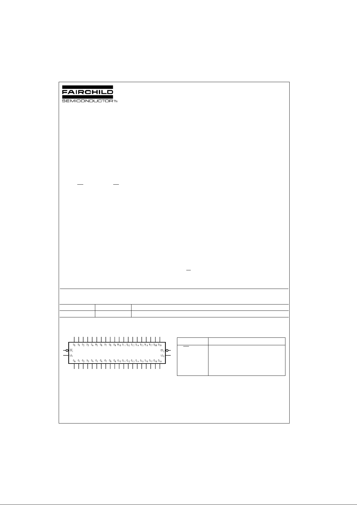
Logic Symbol Pin Descriptions
Order Number Package Number Package Description
74VCX16841MTD MTD56 56-Lead Thin Shrink Small Outline Package (TSSOP), JEDEC MO-153, 6.1mm Wide
Pin Names Description
OE
n
Output Enable Input (Active LOW)
LE
n
Latch Enable Input
D
0–D19
Inputs
O
0–O19
Outputs
Page 2
www.fairchildsemi.com 2
74VCX16841
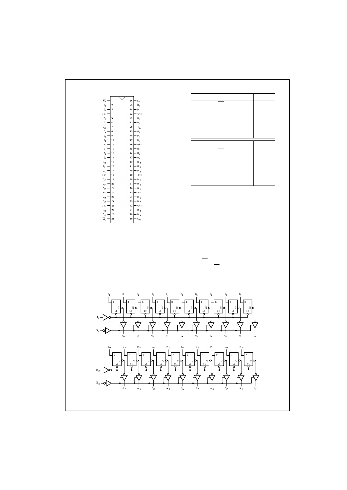
Connection Diagram Tr uth Tables
H = HIGH Voltage Level
L = LOW Voltage Level
X = Immaterial (HIGH or LOW, inputs may not float)
Z = High Impedance
O0 = Previous O0 before HIGH-to-LOW of Latch Enable
Functional Description
The 74VCX16841 contai ns twenty D-type latches with 3STATE outputs. The device is byte controlled with each
byte functioning iden tically, but indepe ndent of the other.
Control pins can be shorted togeth er to obtain full 20-bit
operation. The following description applies to each byte.
When the Latch Enable (LE
n
) input is HIGH, data on the D
n
enters the latches. I n this condition the latches are transparent, i.e., a latch output will chan ge states each time its
D-type input changes. When LE
n
is LOW, the latches store
information that was presen t on the D-type inputs a setup
time preceding the HI GH -to -L OW tr ans i tion on LE
n
. The 3-
STATE outputs are controlled by the Output Enable (OE
n
)
input. When OE
n
is LOW the standard outputs are in the 2-
state mode. When OE
n
is HIGH, the standard outputs a re
in the high impedance mode but this does not interfere with
entering new data into the latches.
Logic Diagram
Please note that this diagram is provided o nly f or t he understanding o f lo gic operations and shou ld not be used to estimate propagation delays.
Inputs Outputs
LE
1
OE
1
D0–D9O0–O
9
XHXZ
HLL L
HLHH
LLXO
0
Inputs Outputs
LE
2
OE2D10–D19O10–O
19
XHXZ
HLL L
HLHH
LLXO
0
Page 3

3 www.fairchildsemi.com
74VCX16841
Absolute Maximum Ratings(Note 2) Recommended Operating
Conditions
(Note 4)
Note 2: The Absolute Maximum Ratings are those values beyond which
the safety of the device cannot be guaranteed. The device should not be
operated at these limits. The parametric values defined in the Electrical
Characteristics tables are not guaranteed at the Absolute Maximum Rat-
ings. The “Recommended Operating Conditions” table will define the conditions for actual device operation.
Note 3: I
O
Absolute Maximum Rating must be observed.
Note 4: Floating or unused inputs m us t be held HIGH or LOW.
DC Electrical Characteristics (2.7V < VCC ≤ 3.6V)
Note 5: Outputs disab led or 3-STATE only.
Supply Voltage (VCC) −0.5V to +4.6V
DC Input Voltage (V
I
) −0.5V to +4.6V
Output Voltage (V
O
)
Outputs 3-STATE −0.5V to +4.6V
Outputs Active (Note 3) −0.5V to V
CC
+ 0.5V
DC Input Diode Current (I
IK
) VI < 0V −50 mA
DC Output Diode Current (I
OK
)
V
O
< 0V −50 mA
V
O
> V
CC
+50 mA
DC Output Source/Sink Current
(I
OH/IOL
) ±50 mA
DC V
CC
or GND Current per
Supply Pin (I
CC
or GND) ±100 mA
Storage Temperature Range (T
STG
) −65°C to +150°C
Power Supply
Operating 1.65V to 3.6V
Data Retention Only 1.2V to 3.6V
Input Voltage −0.3V to +3.6V
Output Voltage (V
O
)
Output in Active States 0V to V
CC
Output in “OFF” State 0.0V to 3.6V
Output Current in I
OH/IOL
VCC = 3.0V to 3.6V ±24 mA
V
CC
= 2.3V to 2.7V ±18 mA
V
CC
= 1.65V to 2.3V ±6 mA
Free Air Operating Temperature
(T
A
) −40°C to +85°C
Minimum Input Edge Rate (∆t/∆V)
V
IN
= 0.8V to 2.0V, VCC = 3.0V 10 ns/V
Symbol Parameter Conditions
V
CC
(V)
Min Max Units
V
IH
HIGH Level Input Voltage 2.7 − 3.6 2.0 V
V
IL
LOW Level Input Voltage 2.7 − 3.6 0.8 V
V
OH
HIGH Level Output Voltage IOH = −100 µA 2.7 − 3.6 VCC − 0.2 V
IOH = −12 mA 2.7 2.2 V
IOH = −18 mA 3.0 2.4 V
IOH = −24 mA 3.0 2.2 V
V
OL
LOW Level Output Voltage IOL = 100 µA 2.7 − 3.6 0.2 V
IOL = 12 mA 2.7 0.4 V
IOL = 18 mA 3.0 0.4 V
IOL = 24 mA 3.0 0.55 V
I
I
Input Leakage Current 0 ≤ VI ≤ 3.6V 2.7 − 3.6 ±5.0 µA
I
OZ
3-STATE Output Leakage 0 ≤ VO ≤ 3.6V
2.7 − 3.6 ±10 µA
VI = VIH or V
IL
I
OFF
Power-OFF Leakage Current 0 ≤ (VI, VO) ≤ 3.6V 0 10 µA
I
CC
Quiescent Supply Current VI = VCC or GND 2.7 − 3.6 20 µA
VCC ≤ (VI, VO) ≤ 3.6V (Note 5) 2.7 − 3.6 ±20 µA
∆I
CC
Increase in ICC per Input VIH = VCC −0.6V 2.7 − 3.6 750 µA
Page 4

www.fairchildsemi.com 4
74VCX16841
DC Electrical Characteristics (2.3V ≤ VCC ≤ 2.7V)
Note 6: Outputs dis abled or 3-STATE only.
DC Electrical Characteristics (1.65V ≤ VCC < 2.3V)
Note 7: Outputs dis abled or 3-STATE only.
Symbol Parameter Conditions
V
CC
(V)
Min Max Units
V
IH
HIGH Level Input Voltage 2.3 − 2.7 1.6 V
V
IL
LOW Level Input Voltage 2.3 − 2.7 0.7 V
V
OH
HIGH Level Output Voltage IOH = −100 µA 2.3 − 2.7 VCC − 0.2 V
IOH = −6 mA 2.3 2.0 V
IOH = −12 mA 2.3 1.8 V
IOH = −18 mA 2.3 1.7 V
V
OL
LOW Level Output Voltage IOL = 100 µA 2.3 − 2.7 0.2 V
IOL = 12 mA 2.3 0.4 V
IOL = 18 mA 2.3 0.6 V
I
I
Input Leakage Current 0 ≤ VI ≤ 3.6V 2.3 − 2.7 ±5.0 µA
I
OZ
3-STATE Output Leakage 0 ≤ VO ≤ 3.6V
2.3 − 2.7 ±10 µA
VI = VIH or V
IL
I
OFF
Power-OFF Leakage Current 0 ≤ (VI, VO) ≤ 3.6V 0 10 µA
I
CC
Quiescent Supply Current VI = VCC or GND 2.3 − 2.7 20 µA
VCC ≤ (VI, VO) ≤ 3.6V (Note 6) 2.3 − 2.7 ±20 µA
Symbol Parameter Conditions
V
CC
(V)
Min Max Units
V
IH
HIGH Level Input Voltage 1.65 - 2.3 0.65 × V
CC
V
V
IL
LOW Level Input Voltage 1.65 - 2.3 0.35 × V
CC
V
V
OH
HIGH Level Output Voltage IOH = −100 µA 1.65 - 2.3 VCC − 0.2 V
IOH = −6 mA 1.65 1.25 V
V
OL
LOW Level Output Voltage IOL = 100 µA 1.65 - 2.3 0.2 V
IOL = 6 mA 1.65 0.3 V
I
I
Input Leakage Current 0 ≤ VI ≤ 3.6V 1.65 - 2.3 ±5.0 µA
I
OZ
3-STATE Output Leakage 0 ≤ VO ≤ 3.6V
1.65 - 2.3 ±10 µA
VI = VIH or V
IL
I
OFF
Power-OFF Leakage Current 0 ≤ (VI, VO) ≤ 3.6V 0 10 µA
I
CC
Quiescent Supply Current VI = VCC or GND 1.65 - 2.3 20 µA
VCC ≤ (VI, VO) ≤ 3.6V (Note 7) 1.65 - 2.3 ±20 µA
Page 5

5 www.fairchildsemi.com
74VCX16841
AC Electrical Characteristics (Note 8)
Note 8: For CL = 50 PF, add approximately 300 ps to the AC maximum specification.
Note 9: Skew is def ined as the absol ut e v alue of the differen c e between the actu al propagation del ay f or any two separat e outputs of the same device. The
specification applies t o any outputs switching in the same direction, either HIGH-to-LOW (t
OSHL
) or LOW-to-HIGH (t
OSLH
).
Dynamic Switching Characteristics
Capacitance
Symbol Parameter
TA = −40°C to +85°C, CL = 30 pF, RL = 500Ω
UnitsV
CC
= 3.3V ± 0.3V V
CC
= 2.5V ± 0.2V V
CC
= 1.8 ± 0.15V
Min Max Min Max Min Max
t
PHL
, t
PLH
Prop Delay Dn to O
n
0.8 3.0 1.0 3.4 1.5 6.8 ns
t
PHL
, t
PLH
Prop Delay LE to O
n
0.8 3.5 1.0 4.4 1.5 8.8 ns
t
PZL
, t
PZH
Output Enable Time 0.8 3.8 1.0 4.9 1.5 9.8 ns
t
PLZ
, t
PHZ
Output Disable Time 0.8 3.7 1.0 4.2 1.5 7.6 ns
t
S
Setup Time 1.5 1.5 2.5 ns
t
H
Hold Time 1.0 1.0 1.0 ns
t
W
Pulse Width 1.5 1.5 4.0 ns
t
OSHL
Output to Output Skew
0.5 0.5 0.75 ns
t
OSLH
(Note 9)
Symbol Parameter Conditions
V
CC
(V)
TA = +25°C
Units
Typical
V
OLP
Quiet Output Dynamic Peak V
OL
CL = 30 pF, VIH = VCC, VIL = 0V 1.8 0.25
V2.5 0.6
3.3 0.8
V
OLV
Quiet Output Dynamic Valley V
OL
CL = 30 pF, VIH = VCC, VIL = 0V 1.8 −0.25
V2.5 −0.6
3.3 −0.8
V
OHV
Quiet Output Dynamic Valley V
OH
CL = 30 pF, VIH = VCC, VIL = 0V 1.8 1.5
V2.5 1.9
3.3 2.2
Symbol Parameter Conditions
TA = +25°C
Units
Typical
C
IN
Input Capacitance VCC = 1.8V, 2.5V or 3.3V, VI = 0V or V
CC
6pF
C
OUT
Output Capacitance VI = 0V or VCC, VCC = 1.8V, 2.5V or 3.3V 7 pF
C
PD
Power Dissipation Capacitance VI = 0V or VCC, f = 10 MHz, 20 pF
VCC = 1.8V, 2.5V or 3.3V
Page 6

www.fairchildsemi.com 6
74VCX16841
AC Loading and Waveforms
FIGURE 1. AC Test Circuit
FIGURE 2. Waveform for Inverting and
Non-Inverting Functions
FIGURE 3. 3-STATE Output High Enable and
Disable Times for Low Voltage Logic
FIGURE 4. 3-STATE Output Low Enable and Disable Times for Low Voltage Logic
FIGURE 5. Propagation Delay, Pulse Width and
t
rec
Waveforms
FIGURE 6. Setup Time, Hold Time and
Recovery Time for Low Voltage Logic
TEST SWITCH
t
PLH
, t
PHL
Open
t
PZL
, t
PLZ
6V at VCC = 3.3 ± 0.3V;
V
CC
x 2 at VCC = 2.5 ± 0.2V; 1.8V ± 0.15V
t
PZH
, t
PHZ
GND
Symbol
V
CC
3.3V ± 0.3V 2.5V ± 0.2V 1.8V ± 0.15V
V
mi
1.5V VCC/2 VCC/2
V
mo
1.5V VCC/2 VCC/2
V
X
VOL + 0.3V VOL + 0.15V VOL + 0.15V
V
Y
VOH − 0.3V VOH − 0.15V VOH − 0.15V
Page 7

Fairchild does not assume any responsibility for use of any circuitry described, no circuit patent licenses are implied and Fairchild reserves the right at any time without notice to change said circuitry and specifications.
74VCX16841 Low Voltage 20-Bit Transparent Latch with 3.6V Tolerant Inputs and Outputs
LIFE SUPPORT POLICY
FAIRCHILD’S PRODUCTS ARE NOT AUTHORIZED FOR USE AS CRITICAL COMPONENTS IN LIFE SUPPORT
DEVICES OR SYSTEMS WITHOUT THE EXPRESS WRITTEN APPROVAL OF THE PRESIDENT OF FAIRCHILD
SEMICONDUCTOR CORPORATION. As used herein:
1. Life support devices or system s are de vices o r syste ms
which, (a) are intended for surgical implant into the
body, or (b) support or sustain life, and (c) whose failure
to perform when properly used in accordance with
instructions for use provide d in the lab el ing , can be re asonably expected to result in a significant in jury to the
user.
2. A critical component in any component of a life support
device or system whose failure to perform can be r easonably expected to cau se th e f ail ur e o f the life sup por t
device or system, or to affect its safety or effectiveness.
www.fairchildsemi.com
Physical Dimensions inches (millimeters) unless otherwise noted
56-Lead Thin Shrink Small Outline Package (TSSOP), JEDEC MO-153, 6.1mm Wide
Package Number MTD56
 Loading...