

Datasheet 74VCX1632245TTR, 74VCX1632245TBR, 74VCX1632245TB, 74VCX1632245LBR, 74VCX1632245LB Datasheet (SGS Thomson Microelectronics)
Page 1
1/15September 2003
■ HIGH SPEED: t
PD
= 4.4ns (MAX.) a t TA=85°C
V
CCA
=3.0VV
CCB
=2.3V
■ LOW POWER DISSIPATION:
I
CCA=ICCB
=20µA(MAX.) at TA=85°C
■ SYMMETRICAL OUTPUT IMPEDANCE:
|I
OHA
|=I
OLA
= 8mA MIN at
V
CCA
=3.0VV
CCB
= 1.65V or 2.3V
|I
OHA
|=I
OLA
= 18m A MIN at
V
CCA
=2.3VV
CCB
= 1.65V)
■ BALANCED PROPAGATION DELAYS:
t
PLH
≅ t
PHL
■ POWER DOWN P ROTECTION ON I NP UTS
AND OUTPUTS
■ 26ΩSERIESRESISTOR ONASIDEOUTPUTS
■ OPERATING VOLTAGE RANGE:
V
CCA
(OPR) = 2.3V to 3.6V (1.2V Data
Retention)
V
CCB
(OPR) = 1.65V to 2.7V (1.2V Data
Retention)
■ PIN AND FUNCTION COMPATIBLE WITH
74 SERIES 16245
■ LATCH-UP PERFORMANCE EXCEEDS
500mA (JESD 17)
■ ESD PERFORM ANCE :
HBM > 2000V (MIL STD 883 method 3015);
MM > 200V
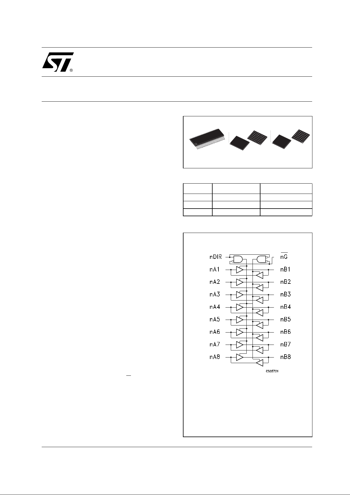
DESCRIPTION
The 74VCX1632245 is a dual supply low voltage
CMOS 16-BIT BUS TRANSCEIVER fabricated
with sub-micron sil icon gate and five-layer metal
wiring C
2
MOS technology . Designed for use as an
interface between a 3.3V bus and a 2.5V or 1.8V
bus in a mixed 3.3V/1.8V,3.3V/2.5V and 2.5V/
1.8V supply syste ms, it achieves high speed
operation while maintaining the CMOS low power
dissipation.
This IC is intended f or two-way asynchronous
communication between data buses and the
direction of data transmission is determined by
nDIR inputs. The enable inputs nG
canbeusedto
disable the device so that the bus es are effectively
isolated. The A-port interfaces with the 3V bus, the
B-port with the 2.5V and 1.8 V bus.
All inputs are equipped with protection circuits
against static discharge, giving them 2KV ESD immunity and transient excess voltage. A ll floating
bus t erminals during High Z State must be held
HIGH or LOW.
74VCX1632245
16-BIT DUAL SUPPLY BUS TRANSCEIVER
LEVEL TRANSLATOR WITH A SIDE SERIES RESISTOR
ORDER CO DES
PACKAGE TRAY T & R
TSSOP48 74VCX1632245TTR
TFBGA54 74VCX1632245LB 74VCX1632245LBR
µTFBGA42 74VCX1632245TB 74VCX1632245TBR
TSSOP µTFBGATFBGA
LOGIC DIAGRAM
n = 1, 2
Page 2
74VCX1632245
2/15
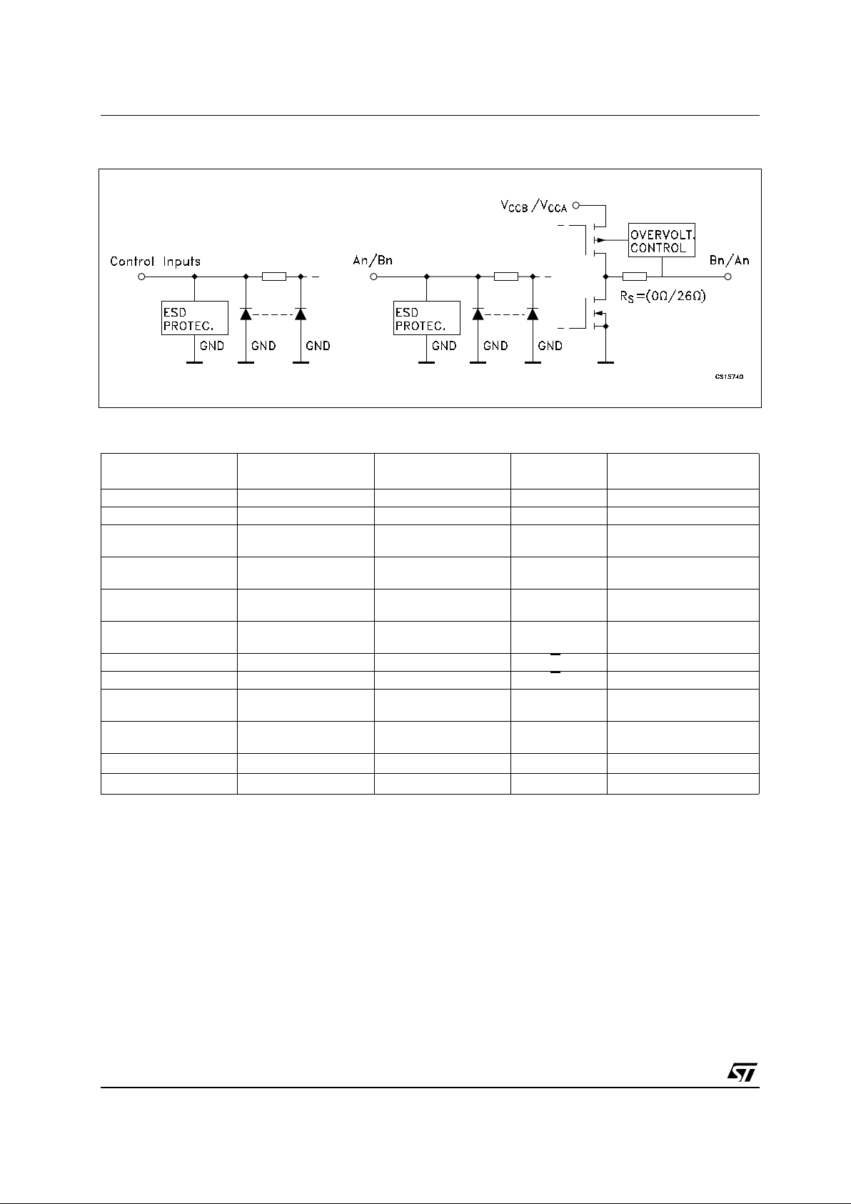
INPUT AND OUTPUT EQ UIVALENT CIRCUIT
PIN DESCRIPTION
TFBGA54 PIN N
o
µTFBGA42 PIN N
o
TSSOP PIN N
o
SYMBOL NAME AND FUNCTION
A3 B3 1 1DIR Directional Controls
J3 F3 24 2DIR Directional Controls
A6, B5, B6, C5,
C6, D5, D6, E5
A4, A5, A6, B5,
B6, C5, C6, D5
47, 46, 44, 43,
41, 40, 38, 37
1A1 to 1A8 Data Inputs/Outputs
E6, F5, F6,G5,
G6, H5, H6, J6
D6, E5, E6, F5,
F6,G4, G5, G6
36, 35, 33, 32,
30, 29, 27, 26
2A1 to 2A8 Data Inputs/Outputs
A1, B2, B1, C2,
C1, D2, D1, E2
A3, A2, A1, B2,
B1, C2, C1, D2
2, 3, 5, 6,
8, 9, 11, 12
1B1 to 1B8 Data Inputs/Outputs
E1, F2, F1,G2,
G1, H2, H1, J1
D1, E2, E1, F2,
F1,G3, G2, G1
13, 14, 16, 17,
19, 20, 22, 23
2B1 to 2B8 Data Inputs/Outputs
J4 F4 25 G
2 Output Enable Inputs
A4 B4 48 G
1 Output Enable Inputs
D3, D4, E3, E4,
F3, F4
C3, C4, E3, E4 4, 10, 15, 21,
28, 34, 39, 45
GND Ground (0V)
A2, A5, B3, B4,
H3, H4, J2, J5
- - NC No Connected
C4, G4 D4 42, 31 V
CCA
Positive Supply Voltage
C3,G3 D3 7,18 V
CCB
Positive Supply Voltage
Page 3
74VCX1632245
3/15
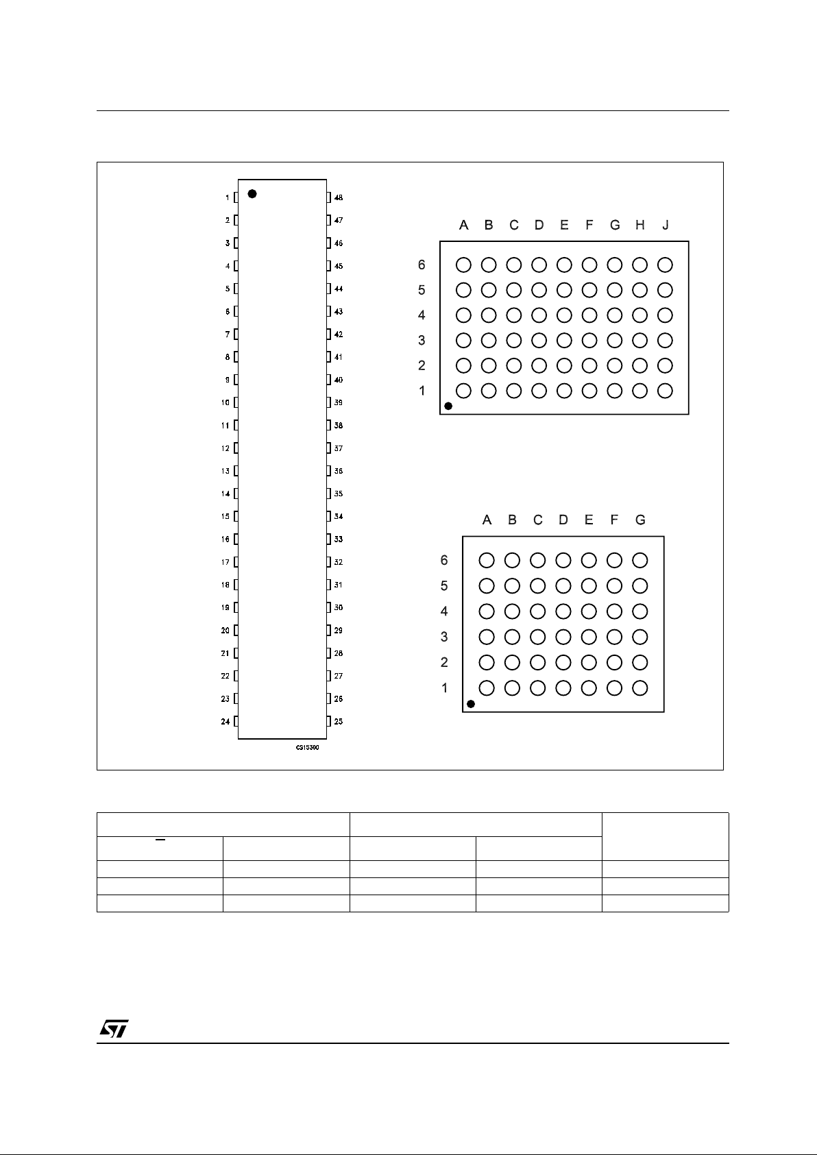
PIN CONNECTION (top view for TSSOP, top through view for BGA )
TRUTH T ABLE
X=Don’t care; Z=High Impedance
INPUTS FUNCTION
OUTPUT
G
DIR A BUS B BUS
L L OUTPUT INPUT A = B
L H INPUT OUTPUT B = A
HXZZZ
TSSOP TFBGA
µTFBGA
Page 4
74VCX1632245
4/15
ABSOLUTE MAXIMUM RATINGS
Absolute Maximum Ratings are those value beyond which damage to the device may occur. Functional operation under these conditions is
not implied
RECOMMENDED OPERATING CONDITIONS
1) VINfrom0.8Vto 2.0V at VCC=3.0V
Symbol Parameter Value Unit
V
CCA
Supply Voltage
-0.5 to +4.6 V
V
CCB
Supply Voltage
-0.5 to +4.6 V
V
I
DC Input Voltage
-0.5 to +4.6 V
V
I/OA
DC I/O Voltage (Output disabled)
-0.5 to +4.6 V
V
I/OB
DC I/O Voltage (Output disabled)
-0.5 to +4.6 V
V
I/OA
DC I/O Voltage -0.5 to V
CCA
+ 0.5
V
V
I/OB
DC I/O Voltage -0.5 to V
CCB
+ 0.5
V
I
IK
DC Input Diode Current
− 20 mA
I
OK
DC Output Diode Current
− 50 mA
I
OA
DC Output Current
± 50 mA
I
OB
DC Output Current
± 50 mA
I
CCA
DC VCCor Ground Current
± 100 mA
I
CCB
DC VCCor Ground Current
± 100 mA
P
d
Power Dissipation
400 mW
T
stg
Storage Temperature
-65 to +150 °C
T
L
Lead Temperature (10 sec)
300 °C
Symbol Parameter Value Unit
V
CCA
Supply Voltage
2.3 to 3.6 V
V
CCB
Supply Voltage
1.65 to 2.7 V
V
I
Input Voltage (Dir, G) 0 to V
CCB
V
V
I/OA
I/O Voltage 0 to V
CCA
V
V
I/OB
I/O Voltage 0 to V
CCB
V
T
op
Operating Temperature
-40 to 85 °C
dt/dv Input Rise and Fall Time (note 1) 0 to 10 ns/V
Page 5
74VCX1632245
5/15
DC SPEC IFICATION FOR V
CCA
(*) VCCrange = 3.3±0.3; 2.5±0.2V; 1.8±0.15V
Symbol Parameter
Test Condition Value
Unit
V
CCB
(*)
(V)
V
CCA
(*)
(V)
T
A
=25°C
-40 to 85 °C
Min. Typ. Max. Min. Max.
V
IHA
High Level Input
Voltage (An)
1.8 2.5 1.6 1.6
V1.8 3.3 2.0 2.0
2.5 3.3 2.0 2.0
V
ILA
Low Level Input
Voltage (An)
1.8 2.5 0.7 0.7
V1.8 3.3 0.8 0.8
2.5 3.3 0.8 0.8
V
OHA
High Level
Output Voltage
2.3 3.0
IO=-100µA
2.8 2.8
V
2.3 3.0
I
O
=-8mA
2.4 2.4
1.65 3.0
I
O
=-8mA
2.4 2.4
1.65 2.3
I
O
=-6mA
1.8 1.8
V
OLA
Low Level
Output Voltage
2.3 3.0
IO=100µA
0.2 0.2
V
2.3 3.0
I
O
=8mA
0.55 0.55
1.65 3.0
I
O
=8mA
0.55 0.55
1.65 2.3
I
O
=6mA
0.40 0.40
I
IA
Input Leakage
Current
2.7 3.6
V
I=VCC
or GND
± 0.5 ± 5 µA
I
OZA
High Impedance
Output Leakage
Current
2.7 3.6 V
IA
= GND or 3.6V
V
IB=VIHB
or V
ILB
G =V
CCB
± 1.0 ± 10 µA
I
OFF
Power Off
Leakage Current
00VIA= GND to 3.6V
V
IB
=GND to3.6V
G
, Dir = GND to
3.6V
± 1.0 ± 10 µA
I
CCtA
Quiescent
Supply Current
1.95 3.6
V
IA=VCCA
or GND
V
IB=VCCB
or GND
220µA
1.95 2.7
2.7 3.6
∆I
CCtA
Maximum
Quiescent
Supply Current /
Input (An)
2.7 3.6
V
IA=VCCA
-0.6V
V
IB=VCCB
or GND
0.75 mA
1.95 3.6
1.95 2.7
Page 6

74VCX1632245
6/15
DC SPEC IFICATION FOR V
CCB
(*) VCCrange = 3.3±0.3; 2.5±0.2V; 1.8±0.15V
Symbol Parameter
Test Condition Value
Unit
V
CCB
(V)
(*)
V
CCA
(V)
(*)
T
A
=25°C
-40 to 85 °C
Min. Typ. Max. Min. Max.
V
IHB
High Level Input
Voltage (Bn, Dir,
G
)
1.8 2.5
0.65V
CCB
0.65V
CCB
V
1.8 3.3
0.65V
CCB
0.65V
CCB
2.5 3.3 1.6 1.6
V
ILB
Low Level Input
Voltage (Bn, Dir,
G
)
1.8 2.5
0.35V
CCB
0.35V
CCB
V
1.8 3.3
0.35V
CCB
0.35V
CCB
2.5 3.3 0.7 0.7
V
OHB
High Level
Output Voltage
2.3 3.0
IO=-100µA
2.1 2.1
V
2.3 3.0
I
O
=-18mA
1.7 1.7
1.65 3.0
I
O
=-6mA
1.25 1.25
1.65 2.3
I
O
=-6mA
1.25 1.25
V
OLB
Low Level
Output Voltage
2.3 3.0
IO=100µA
0.2 0.2
V
2.3 3.0
I
O
=18mA
0.60 0.60
1.65 3.0
I
O
=6mA
0.30 0.30
1.65 2.3
I
O
=6mA
0.30 0.30
I
IB
Input Leakage
Current
2.7 3.6
V
I=VCC
or GND
± 0.5 ± 5 µA
I
OZB
High Impedance
Output Leakage
Current
2.7 3.6 V
IA=VIHA
or V
ILA
VIB= GND or 2.7V
G
=V
CCB
± 1.0 ± 10 µA
I
CCtB
Quiescent
Supply Current
1.95 3.6 VIA=V
CCA
or GND
V
IB=VCCB
or GND
Dir or G
=V
CCB
or
GND
220µA
1.95 2.7
2.7 3.6
∆I
CCtB
Maximum
Quiescent
Supply Current /
Input (Bn, DIR,
G
)
2.7 3.6
V
IB=VCCB
-0.6V
V
IA=VCCA
or GND
0.75 mA
1.95 3.6
1.95 2.7
Page 7

74VCX1632245
7/15
DYNAMIC SWITCHING CHARACTERISTICS
Symbol Parameter
Test Condition Value
Unit
V
CCB
(V)
V
CCA
(V)
T
A
=25°C
-40to85°C
Min. Typ. Max. Min. Max.
V
OLPA
Dynamic Low Level
Quiet An Output
1.8 2.5
C
L
=30pF
V
IL
=0V VIH=V
CC
0.25
V1.8 3.3 0.35
2.5 3.3 0.35
V
OLPB
Dynamic Low Level
Quiet Bn Output
1.8 2.5
C
L
=30pF
V
IL
=0V VIH=V
CC
0.25
V1.8 3.3 0.25
2.5 3.3 0.6
V
OLVA
Dynamic Low Level
Quiet An Output
1.8 2.5
C
L
=30pF
V
IL
=0V VIH=V
CC
-0.25
V1.8 3.3 -0.35
2.5 3.3 -0.35
V
OLVB
Dynamic Low Level
Quiet Bn Output
1.8 2.5
C
L
=30pF
V
IL
=0V VIH=V
CC
-0.25
V1.8 3.3 -0.25
2.5 3.3 -0.6
V
OHVA
Dynamic Low Level
Quiet An Output
1.8 2.5
C
L
=30pF
V
IL
=0V VIH=V
CC
2.1
V1.8 3.3 2.6
2.5 3.3 2.6
V
OHVB
Dynamic Low Level
Quiet Bn Output
1.8 2.5
C
L
=30pF
V
IL
=0V VIH=V
CC
1.7
V1.8 3.3 1.7
2.5 3.3 2.0
Page 8

74VCX1632245
8/15
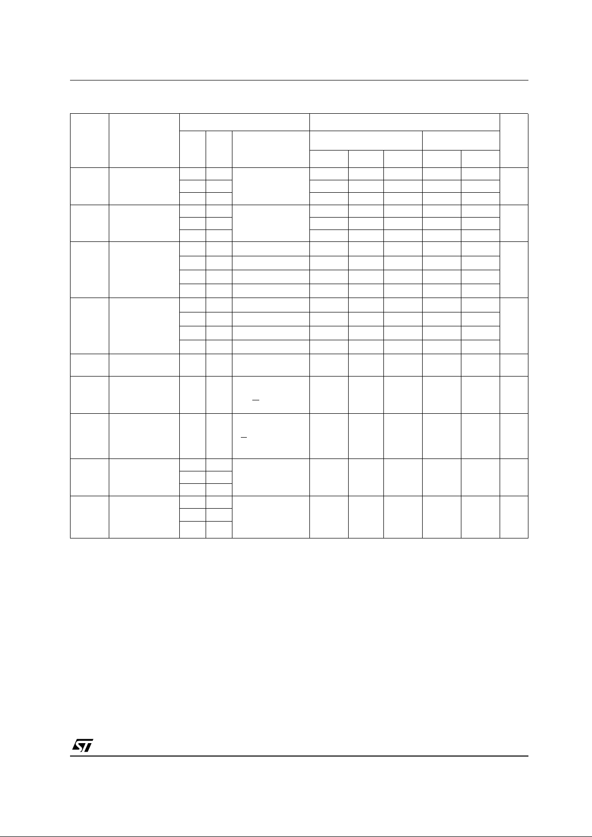
AC ELECTRICAL CHARACTERISTICS
1) Skew is defined as the absolute value of the difference between the actual propagation delay for any two outputs of the same device
switching in the same direction, either HIGH or LOW (t
OSLH
=|t
PLHm-tPLHn
|, t
OSHL
=|t
PHLm-tPHLn
|
2) Parameter guaranteed by design
CAPACITANCE CHARACT ERISTICS
1) CPDis defined as the value of the IC’s internal equivalent capacitance which is calculated from the operating current consumption without
load. (Refer to Test Circuit). Average current can be obtained by the following equation. I
CC(opr)=CPDxVCCxfIN+ICC
/16 (per circuit)
Symbol Parameter
Test Condition Value
Unit
V
CCB
(V)
V
CCA
(V)
-40 to 85 °C
Min. Max.
t
PLHtPHL
Propagation Delay Time
An to Bn
1.8± 0.15 2.5 ± 0.2
C
L
=30pF
R
L
=500Ω
1.0 5.8
ns1.8 ± 0.15 3.3 ± 0.3 1.0 6.2
2.5 ± 0.2 3.3 ± 0.3 1.0 4.4
t
PLHtPHL
Propagation Delay Time
Bn to An
1.8± 0.15 2.5 ± 0.2
C
L
=30pF
R
L
=500Ω
1.0 5.5
ns1.8 ± 0.15 3.3 ± 0.3 1.0 5.1
2.5 ± 0.2 3.3 ± 0.3 1.0 4.0
t
PZLtPZH
Output Enable Time
G
to An
1.8± 0.15 2.5 ± 0.2
C
L
=30pF
R
L
=500Ω
1.0 5.3
ns1.8 ± 0.15 3.3 ± 0.3 1.0 5.1
2.5 ± 0.2 3.3 ± 0.3 1.0 4.0
t
PZLtPZH
Output Enable Time
G
to Bn
1.8± 0.15 2.5 ± 0.2
C
L
=30pF
R
L
=500Ω
1.0 8.3
ns1.8 ± 0.15 3.3 ± 0.3 1.0 8.2
2.5 ± 0.2 3.3 ± 0.3 1.0 4.6
t
PLZtPHZ
Output Disable Time
G
to An
1.8± 0.15 2.5 ± 0.2
C
L
=30pF
R
L
=500Ω
1.0 5.2
ns1.8 ± 0.15 3.3 ± 0.3 1.0 5.6
2.5 ± 0.2 3.3 ± 0.3 1.0 4.8
t
PLZtPHZ
Output Disable Time
G
to Bn
1.8± 0.15 2.5 ± 0.2
C
L
=30pF
R
L
=500Ω
1.0 4.6
ns1.8 ± 0.15 3.3 ± 0.3 1.0 4.5
2.5 ± 0.2 3.3 ± 0.3 1.0 4.4
t
OSLH
t
OSHL
Output ToOutput Skew
Time (note1, 2)
1.8± 0.15 2.5 ± 0.2
C
L
=30pF
R
L
=500Ω
0.5
ns1.8 ± 0.15 3.3 ± 0.3 0.5
2.5 ± 0.2 3.3 ± 0.3 0.75
Symbol Parameter
Test Condition Value
Unit
V
CCB
(V)
V
CCA
(V)
T
A
=25°C
-40to85°C
Min. Typ. Max. Min. Max.
C
INB
Input Capacitance open open 5 pF
C
I/O
Input/Output
Capacitance
2.5 3.3 6 pF
C
PD
Power Dissipation
Capacitance
2.5 3.3 f=10MHz 28 pF
1.8 3.3 28 pF
Page 9

74VCX1632245
9/15
TEST CIRCUIT
CL= 30pF or equivalent (includes jig and probe capacitance)
R
L=R1
=500Ωor equivalent
R
T=ZOUT
of pulse generator (typically 50Ω)
WAVEFORM SYMBOL VALUE
TEST SWITCH
t
PLH,tPHL
Open
t
PZL,tPLZ(VCC
= 3.0 to 3.6V)
6V
t
PZL,tPLZ(VCC
= 2.3 to 2.7V or VCC= 1.65 to 1.95V) 2V
CC
t
PZH,tPHZ
GND
Symbol
V
CC
3.0 to 3.6V 2.3 to 2.7V 1.65 to 1.95V
V
IH
V
CC
V
CC
V
CC
V
M
1.5V VCC/2 VCC/2
V
X
VOL+0.3V VOL+0.15V VOL+0.15V
V
Y
VOL-0.3V VOL-0.15V VOL-0.15V
Page 10

74VCX1632245
10/15
WAVEFORM 1: PROPAGATION DELAY (f=1MHz; 50% duty cycle)
WAVEFORM 2: OUTPUT ENABLE AND DISABLE TIME (f=1MHz; 50% duty cycle)
Page 11

74VCX1632245
11/15
DIM.
mm. inch
MIN. TYP MAX. MIN. TYP. MAX.
A 1.2 0.047
A1 0.05 0.15 0.002 0.006
A2 0.9 0.035
b 0.17 0.27 0.0067 0.011
c 0.09 0.20 0.0035 0.0079
D 12.4 12.6 0.488 0.496
E 8.1 BSC 0.318 BSC
E1 6.0 6.2 0.236 0.244
e 0 .5 BSC 0.0197 BSC
K0˚ 8˚0˚ 8˚
L 0.50 0.75 0.020 0.030
TSSOP48 MECHANICAL DATA
c
E
b
A2
A
E1
D
1
PIN 1 IDENTIFICATION
A1
L
K
e
7065588C
Page 12

74VCX1632245
12/15
DIM.
mm. mils
MIN. TYP MAX. MIN. TYP. MAX.
A 1.2 47.2
A1 0.25 9.8
A2 0.78 0.86 30.7 33.8
B 0.35 0.4 0.45 13.7 15.7 17.7
D 7.9 8.1 311.0 318.9
D1 6.4 252.0
E 5.4 5.5 5.6 212.6 216.5 220.5
E1 4 157.5
e 0.8 31.5
SE 0.4 15.7
TFBGA54 MECHANICAL DATA
7390143/C
Page 13

74VCX1632245
13/15
DIM.
mm. mils
MIN. TYP MAX. MIN. TYP. MAX.
A 3.90 4.10 153.5 161.4
B 3.40 3.60 133.9 141.7
C 1.07 1.16 42.1 45.6
D 0.3 11.8
E 0.5 19.7
F 0.78 0.86 30.7 33.9
µTFBGA42 MECHANICAL DATA
Page 14

74VCX1632245
14/15
DIM.
mm. inch
MIN. TYP MAX. MIN. TYP. MAX.
A 330 12.992
C 12.8 13.2 0.504 0.519
D 20.2 0.795
N 60 2.362
T 30.4 1.197
Ao 8.7 8.9 0.343 0.350
Bo 13.1 13.3 0.516 0.524
Ko 1.5 1.7 0.059 0.067
Po 3.9 4.1 0.153 0.161
P 11.9 12.1 0.468 0.476
Tape & Reel TSSOP48 MECHANICAL DATA
Page 15

74VCX1632245
15/15
Information furnished is believed to be accurate and reliable. However, STMicroelectronics assumes no responsibility for the
consequences of use o f suc h info rmat ion n or for any in fring ement of paten ts or oth er ri ghts of th ird p arties which may resul t f rom
its use. No license is granted by implication or otherwise under any patent or patent rights of STMicroelectronics. Specifications
mentioned in this publication are subject to change without notice. This publication supersedes and replaces all information
previously supplied. STMicroelectronics products are not authorized for use as critical components in life support devices or
systems without express written approval of STMicroelectronics.
The ST logo is a registered trademark of STMicroelectronics
All other names are the property of their respective owners
© 2003 STMicroelectronics - All Rights Reserved
STMicroelectronics GROUP OF COMPANIES
Australia - Belgium - Brazil - Canada - China - Czech Republic - Finland - France - Germany - Hong Kong - India - Israel - Italy - Japan -
Malaysia - Malta - Morocco - Singapore - Spain - Sweden - Switzerland - United Kingdom - United States.
http://www.st.com
 Loading...