

Page 1
查询74V2G07供应商
■ HIGH SPEED: t
■ LOW POWER DISSIPATION:
I
= 1µA(MAX.) at TA=25°C
CC
■ HIGH NOISE IMMUNITY:
V
= V
NIH
■ POWER DOWN PROTECTION ON INPUT
■ OPERATING VOLTAGE RANGE:
(OPR) = 2V to 5.5V
V
CC
■ IMPROVED LATCH-UP IMMUNITY
= 28% VCC (MIN.)
NIL
DESCRIPTION
The 74V2G07 is an advanced high-speed CMOS
TRIPLE BUFFER (OPEN DRAIN) fabricated with
sub-micron silicon gate and double-layer metal
wiring C
2
MOS technology.
The internal circuit is composed of 2 stages
including buffer output, which provide high no ise
immunity and stable output.
=3.7ns (TYP.) at VCC = 5V
PD
74V2G0 7
TRIPLE BUFFER (OPEN DRAIN)
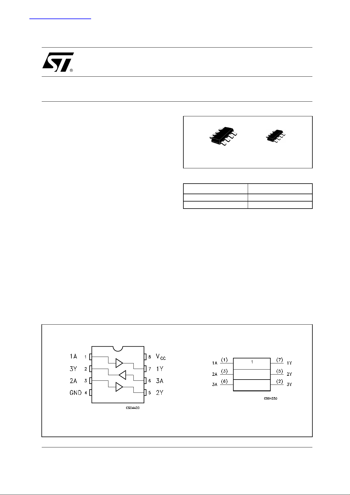
PRELIMINARY DATA
SOT323-8LSOT23-8L
ORDER CODES
PACKAGE T & R
SOT23-8L 74V2G07STR
SOT323-8L 74V2G07CTR
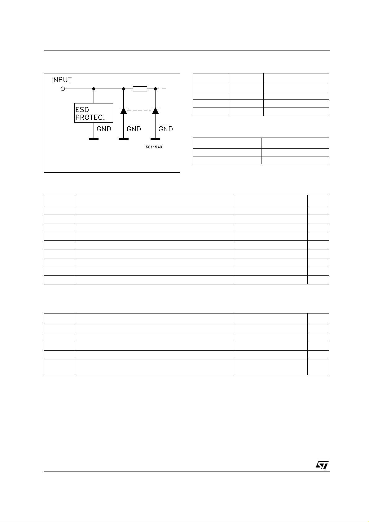
Power down protection is provided on inpu t an d 0
to 7V can be acce pted on inp ut with no rega rd to
the supply voltage. This device can be used to
interface 5V to 3V.
PIN CONNECTION AND IEC LOGIC SYMBOLS
1/9November 2001
This is preliminary information on a new product now in development are or undergoing evaluation. Details subject to change without notice.
Page 2
74V2G07
INPUT EQUIVALENT CIRCUIT PIN DESCRIPTION
PIN No SYMBOL NAME QND FUNCTION
1, 3, 6 1A, 2A, 3A Data Inputs
7, 5, 2 1Y, 2Y, 3Y Data Outputs
4 GND Ground (0V)
8
V
CC
TRUTH TABLE
AY
LL
HZ
Z: High Impedance
ABSOLUTE MAXIMUM RATINGS
Symbol Parameter Value Unit
V
V
V
I
I
OK
I
I
or I
CC
T
T
Absolute Maximum Ratings are those values beyond which damage to the device may occur. Functional operation under these conditions is
not implied.
Supply Voltage
CC
DC Input Voltage
I
DC Output Voltage -0.5 to VCC + 0.5
O
DC Input Diode Current
IK
DC Output Diode Current
DC Output Current
O
DC VCC or Ground Current
GND
Storage Temperature
stg
Lead Temperature (10 sec)
L
Positive Supply Voltage
-0.5 to +7.0 V
-0.5 to +7.0 V
V
- 20 mA
± 20 mA
± 25 mA
± 50 mA
-65 to +150 °C
260 °C
RECOMMENDED OPERATING CONDITIONS
Symbol Parameter Value Unit
V
V
V
T
dt/dv
1) VIN from 30 % to 70% of V
2/9
Supply Voltage
CC
Input Voltage
I
Output Voltage 0 to V
O
Operating Temperature
op
Input Rise and Fall Time (note 1) (V
(V
CC
= 3.3 ± 0.3V)
CC
= 5.0 ± 0.5V)
CC
2 to 5.5 V
0 to 5.5 V
CC
-55 to 125 °C
0 to 100
0 to 20
V
ns/V
ns/V
Page 3
DC SPECIFICATIONS
Symbol Parameter
V
V
V
I
I
High Level Input
IH
Voltage
Low Level Input
IL
Voltage
Low Level Output
OL
Voltage
High Impedance
OZ
Output Leakage
Current
I
Input Leakage
I
Current
Quiescent Supply
CC
Current
Test Condition Value
V
(V)
CC
= 25°C
A
Min. Typ. Max. Min. Max. Min. Max.
-40 to 85°C -55 to 125°C
T
2.0 1.5 1.5 1.5
3.0 to
5.5
0.7V
CC
0.7V
CC
0.7V
CC
2.0 0.5 0.5 0.5
3.0 to
5.5
2.0
3.0
4.5
3.0
4.5
5.5
0 to
5.5
5.5
=50 µA
I
O
I
=50 µA
O
I
=50 µA
O
I
=4 mA
O
I
=8 mA
O
= VIH or V
V
I
IL
VO = VCC or GND
V
= 5.5V or GND
I
= VCC or GND
V
I
0.3V
CC
0.3V
CC
0.0 0.1 0.1 0.1
0.0 0.1 0.1 0.1
0.0 0.1 0.1 0.1
0.36 0.44 0.55
0.36 0.44 0.55
±
0.25
± 2.5 ± 5 µA
± 0.1 ± 1 ± 1 µA
11020µA
74V2G07
Unit
0.3V
CC
V
V
V
AC ELECTRICAL CHARACTERISTICS (Input t
Test Condition Value
Symbol Parameter
t
t
(*) Vol tage range is 3. 3V ± 0.3V
(**) Voltage range is 5.0V ±
Propagation Delay
PZL
Time
Propagation Delay
PLZ
Time
0.5V
3.3
3.3
5.0
5.0
3.3
5.0
C
V
CC
(V)
L
(pF)
(*)
15 4.8 7.7 1.0 9.0 1.0 10.0
(*)
50 5.3 8.5 1.0 10.0 1.0 11.0
(**)
15 3.7 5.5 1.0 6.5 1.0 7.5
(**)
50 4.2 7.5 1.0 8.5 1.0 9.5
(*)
50 7.5 10.5 1.0 11.5 1.0 12.5
(**)
50 4.7 7.5 1.0 8.5 1.0 9.5
= tf = 3ns)
r
= 25°C
T
A
-40 to 85°C -55 to 125°C
Min. Typ. Max. Min. Max. Min. Max.
Unit
ns
ns
3/9
Page 4

74V2G07
CAPACITIVE CHARACTERISTICS
Test Condition Value
= 25°C
Symbol Parameter
T
A
Min. Typ. Max. Min. Max. Min. Max.
C
C
C
Input Capacitance 4 10 10 10 pF
IN
Output
OUT
Capacitance
Power Dissipation
PD
Capacitance
5101010pF
3pF
(note 1)
1) CPD is defined as the value of the IC’s internal equivalent capacitance which is calculated from the operating current consumption without
load. (R ef er to Test Circ ui t). Averag e operatin g current can be obtained by t he following equation. I
TEST CIRCUIT
-40 to 85°C -55 to 125°C
= CPD x VCC x fIN + I
CC(opr)
CC
Unit
CL = 15/50pF or e qui valent (includes jig and probe capacitance)
= 1KΩ or equivalent
R
1
= Z
R
of pulse generator (typically 50Ω)
T
OUT
WAVEFORM: PROPAGATION DELAY (f=1MHz; 50% duty cycle)
4/9
Page 5

74V2G07
SOT23-8L MECHANICAL DATA
mm. mils
DIM.
MIN. TYP MAX. MIN. TYP. MAX.
A 0.90 1.45 35.4 57.1
A1 0.00 0.15 0.0 5.9
A2 0.90 1.30 35.4 51.2
b 0.22 0.38 8.6 14.9
C 0.09 0.20 3.5 7.8
D 2.80 3.00 110.2 118.1
E 2.60 3.00 102.3 118.1
E1 1.50 1.75 59.0 68.8
e0.65 25.6
e1 1.95 76.7
L 0.35 0.55 13.7 21.6
5/9
Page 6

74V2G07
SOT323-8L MECHANICAL DATA
mm. mils
DIM.
MIN. TYP MAX. MIN. TYP. MAX.
A 0.80 1.10 31.5 43.3
A1 0.00 0.10 0.0 3.9
A2 0.80 1.00 31.5 34.9
b 0.13 0.28 5.1 11.0
C 0.10 0.18 3.9 7.1
D 1.80 2.20 70.9 86.6
E 1.80 2.40 70.9 94.5
E1 1.15 1.35 45.3 53.1
e 0.5 19.7
e1 1.5 59.0
L 0.10 0.30 3.9 11.8
6/9
Page 7

Tape & Reel SOT23-xL MECHANICAL DATA
74V2G07
DIM.
MIN. TYP MAX. MIN. TYP. MAX.
A 180 7.086
C 12.8 13.0 13.2 0.504 0.512 0.519
D 20.2 0.795
N 60 2.362
T 14.4 0.567
Ao 3.13 3.23 3.33 0.123 0.127 0.131
Bo 3.07 3.17 3.27 0.120 0.124 0.128
Ko 1.27 1.37 1.47 0.050 0.054 0.0.58
Po 3.9 4.0 4.1 0.153 0.157 0.161
P 3.9 4.0 4.1 0.153 0.157 0.161
mm. inch
7/9
Page 8

74V2G07
Tape & Reel SOT323-xL MECHANICAL DATA
DIM.
MIN. TYP MAX. MIN. TYP. MAX.
A 175 180 185 6.889 7.086 7.283
C 12.8 13 13.2 0.504 0.512 0.519
D 20.2 0.795
N 59.5 60 60.5 2.362
T 14.4 0.567
Ao 2.25 0.088
Bo 2.7 0.106
Ko 1.2 0.047
Po 3.98 4 4.2 0.156 0.157 0.165
P 3.98 4 4.2 0.156 0.157 0.165
mm. inch
8/9
Page 9

74V2G07
Information furnished is believed to be accurate and reliable. H owever, STMicroelectronics assumes no responsibility for t he
consequences of use of such informatio n nor for any infringement of paten ts or o ther rig hts of t hird part ies which ma y result from
its use. No license is granted by implication or otherwise under any patent or patent rights of STMicroelectronics. Specifications
mentioned in this publicatio n are subject to change without notice. This publication supersedes and replaces all information
previousl y suppl ied. STM icroel ectronics produc ts are not auth orized for use as c ritica l compone nts in l ife s upport dev ices or
systems without express written approval of STMicroelectronics.
Australia - Brazil - Canada - China - Finland - France - Germany - Hong Kong - India - Israel - Italy - Japan - Malaysia - Malta - Morocc o
© The ST logo is a registered trademark of STMicroelectronics
© 2001 STMicroelectronics - Printed in Italy - All Rights Reserved
STMicroelectronics GROUP OF COMPANIES
Singapore - Spain - Sweden - Switzerland - United Kingdom - United States.
© http://www.st.com
9/9
Page 10

WWW.ALLDATASHEET.COM
Copyright © Each Manufacturing Company.
All Datasheets cannot be modified without permission.
This datasheet has been download from :
www.AllDataSheet.com
100% Free DataSheet Search Site.
Free Download.
No Register.
Fast Search System.
www.AllDataSheet.com
 Loading...