

Page 1

74V2G00
DUAL 2-INPUT NAND GATE
■ HIGHSPEED:t
■
LOW POWER DISSIPATION:
I
=1 µA (MAX.)at TA=25oC
CC
■
HIGHNOISEIMMUNITY:
V
NIH=VNIL
■ POWERDOWNPROTECTIONON INPUTS
=28%VCC(MIN.)
=3.7ns(TYP.)atVCC=5V
PD
ANDOUTPUTS
■ SYMMETRICALOUTPUTIMPEDANCE:
|I
|=IOL=8 mA(MIN)
OH
■ BALANCEDPROPAGATIONDELAYS:
t
≅ t
PLH
PHL
■
OPERATINGVOLTAGERANGE:
V
(OPR)= 2Vto 5.5V
CC
■ IMPROVEDLATCH-UPIMMUNITY
DESCRIPTION
The 74V2G00 is an advanced high-speed CMOS
DUAL 2-INPUT NAND GATE fabricated with
sub-micron silicon gate and double-layer metal
SOT23-8L
ORDER CODES
PACKAGE TUBE T & R
SOT23-8L 74V2G00STR
wiringC
2
MOS technology.
The internal circuit is composed of 3 stages
including buffer output, which provide high noise
immunityand stable output.
Power down protection is provided on all inputs
and outputs and 0 to 7V can be accepted on
inputs with no regard to the supply voltage. This
devicecan be used to interface5V to 3V.
PIN CONNECTION AND IEC LOGICSYMBOLS
June 2000
1/6
Page 2
74V2G00
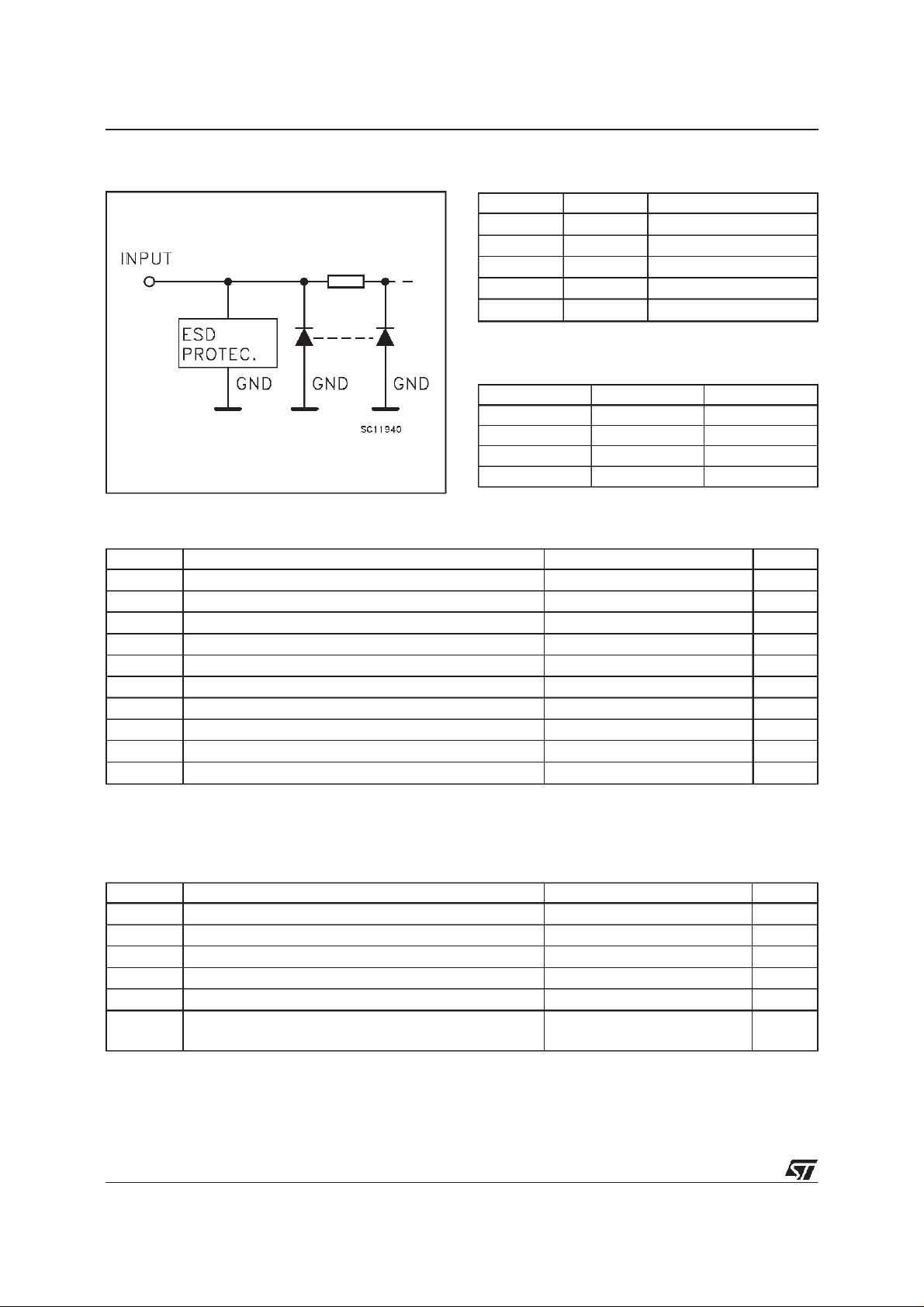
INPUT EQUIVALENTCIRCUIT
PIN DESCRIPTION
PI N No SYMB OL NAME AND F U NCTIO N
1, 5 1A, 2A Data Input
2, 6 1B, 2B Data Input
7, 3 1Y, 2Y Data Output
4 GND Ground (0V)
8V
CC
Positive Supply Voltage
TRUTH TABLE
ABY
LLH
LHH
HLH
HHL
ABSOLUTE MAXIMUM RATINGS
Symb o l Para met er Val u e Uni t
V
V
V
V
I
I
OK
I
or I
I
CC
T
T
AbsoluteMaximumRatingsarethosevaluesbeyondwhichdamageto thedevicemayoccur.Functionaloperation underthesecondition isnotimplied.
=0V
1)V
CC
2)HighorLowState
Supply Voltage -0.5 to +7.0 V
CC
DC Input Voltage -0.5 to +7.0 V
I
DC Output Voltage (see note 1) -0.5 to +7.0 V
O
DC Output Voltage (see note 2) -0.5 to VCC+ 0.5 V
O
DC Input Diode Current - 20 mA
IK
DC Output Diode Current ± 20 mA
DC Output Current ± 25 mA
O
DC VCCor Ground Current ± 50 mA
GND
Storage Temperature -65 to +150
stg
Lead Temperature (10 sec) 260
L
o
C
o
C
RECOMMENDED OPERATING CONDITIONS
Symb o l Para met er Value Un it
V
V
V
V
T
dt/dv
1)VCC=0V
2)HighorLowState
from30%to70%of V
3)V
IN
2/6
Supply Voltage 2.0 to 5.5 V
CC
Input Voltage 0 to 5.5 V
I
Output Voltage (see note 1) 0 to 5.5 V
O
Output Voltage (see note 2) 0 to V
O
Operating Temperature -40 to +85
op
(V
CC
CC
=3.3±0.3V)
=5.0±0.5V)
Input Rise and Fall Time (see note 3) (V
CC
CC
0 to 100
0to20
V
o
C
ns/V
ns/V
Page 3

74V2G00
DC SPECIFICATIONS
Symb o l Para met er Test Condit i o ns Val u e Uni t
T
=25oC -40 to 85oC
A
CC
0.7V
CC
CC
0.3V
CC
V
V
V
V
I
I
OPD
V
CC
(V)
High Level Input
IH
Voltage
Low Level Input
IL
Voltage
High Level Output
OH
Voltage
Low Level Output
OL
Voltage
Input Leakage Current 0 to 5.5 VI= 5.5V or GND ±0.1 ±1.0 µA
I
I
Quiescent Supply
CC
2.0 1.5 1.5
3.0 to 5.5 0.7V
2.0 0.5 0.5
3.0 to 5.5 0.3V
2.0 IO=-50 µA 1.9 2.0 1.9
3.0 I
4.5 I
3.0 I
4.5 I
=-50µA 2.9 3.0 2.9
O
=-50µA 4.4 4.5 4.4
O
=-4 mA 2.58 2.48
O
=-8 mA 3.94 3.8
O
2.0 IO=50 µ A 0.0 0.1 0.1
3.0 I
4.5 I
3.0 I
4.5 I
=50µA 0.0 0.1 0.1
O
=50µA 0.0 0.1 0.1
O
=4 mA 0.36 0.44
O
=8 mA 0.36 0.44
O
5.5 VI=VCCorGND 1 10 µA
Min. Typ. Max. Min. Max.
Current
Output Leakage
0V
= 5.5V 0.5 5.0 µA
OUT
Current
V
V
V
V
AC ELECTRICAL CHARACTERISTICS
(Inputt
r=tf
=3 ns)
Symbol Parameter Test Condition Value Unit
t
Propagation Delay
PLH
t
Time
PHL
(*) Voltagerangeis3.3V±0.3V
(**) Voltagerangeis 5V± 0.5V
V
3.3
3.3
5.0
5.0
CC
(V)
(**)
(**)
C
L
(pF)
(*)
(*)
15 5.5 7.9 1.0 9.5
50 8.0 11.4 1.0 13.0
T
=25oC -40 to 85oC
A
Min. Typ. Max. Min. Max.
ns
15 3.7 5.5 1.0 6.5
50 5.2 7.5 1.0 8.5
CAPACITIVE CHARACTERISTICS
Symb o l Para met er Test Condit i o ns Val u e Uni t
=25oC -40 to 85oC
T
A
Min. Typ. Max. Min. Max.
Input Capacitance 4 10 10 pF
C
IN
Power Dissipation
C
PD
Capacitance (note 1)
1)CPDisdefined asthevalue oftheIC’sinternal equivalentcapacitance whichiscalculatedfromtheoperating currentconsumption without load. (Referto
TestCircuit).Average operatingcurrent canbeobtained bythefollowingequation. I
(opr)= C
CC
19 pF
•
•
f
IN+ICC
/2
V
PD
CC
3/6
Page 4

74V2G00
TESTCIRCUIT
CL= 15/50 pF orequ ivalent (includes jigand probe capacitance)
R
ofpulse generator (typically50Ω)
T=ZOUT
WAVEFORM:PROPAGATIONDELAYS
(f=1MHz;50% duty cycle)
4/6
Page 5

SOT23-8L MECHANICAL DATA
74V2G00
DIM.
MIN. TYP. MAX. MIN. TYP. MAX.
A 0.90 1.45 35.4 57.1
A1 0.00 0.15 0.0 5.9
A2 0.90 1.30 35.4 51.2
b 0.22 0.38 8.6 14.9
C 0.09 0.20 3.5 7.8
D 2.80 3.00 110.2 118.1
E 2.60 3.00 102.3 118.1
E1 1.50 1.75 59.0 68.8
L 0.35 0.55 13.8 21.6
e 0.65 25.6
e1 1.95 76.7
mm mils
5/6
Page 6

74V2G00
Information furnished isbelieved to be accurate and reliable. However, STMicroelectronics assumes no responsibility forthe consequences
of use of such information nor for any infringement of patents or other rights of third parties which may result from its use. No license is
granted by implication or otherwise under any patent or patent rights of STMicroelectronics. Specification mentioned in this publication are
subject tochange without notice. This publication supersedes andreplaces allinformation previously supplied. STMicroelectronics products
are not authorized for use as critical components in lifesupport devices or systems withoutexpress written approval of STMicroelectronics.
The ST logo is a registeredtrademark of STMicroelectronics
2000 STMicroelectronics – Printed in Italy – All Rights Reserved
STMicroelectronics GROUP OF COMPANIES
Australia - Brazil - China - Finland -France - Germany - Hong Kong - India - Italy - Japan- Malaysia - Malta - Morocco
Singapore - Spain- Sweden - Switzerland - UnitedKingdom - U.S.A.
http://www.st.com
.
6/6
 Loading...