

Page 1
74V1T86
SINGLE EXCLUSIVE OR GATE
■ HIGHSPEED:t
■ LOW POWERDISSIPATION:
=1 µA (MAX.) at TA=25oC
I
CC
■ COMPATIBLEWITHTTL OUTPUTS:
V
=2V(MIN),VIL=0.8V(MAX)
IH
■ POWERDOWN PROTECTIONON INPUTS&
=5 ns (TYP.)at VCC=5V
PD
OUTPUT
■ SYMMETRICAL OUTPUTIMPEDANCE:
|I
|=IOL=8 mA(MIN)
OH
■ BALANCEDPROPAGATIONDELAYS:
t
≅ t
PLH
PHL
■ OPERATINGVOLTAGERANGE:
(OPR)= 4.5V to 5.5V
V
CC
■ IMPROVEDLATCH-UP IMMUNITY
DESCRIPTION
The 74V1T86 is an advancedhigh-speed CMOS
SINGLE EXCLUSIVE OR GATE fabricated with
sub-micron silicon gate and double-layer metal
S
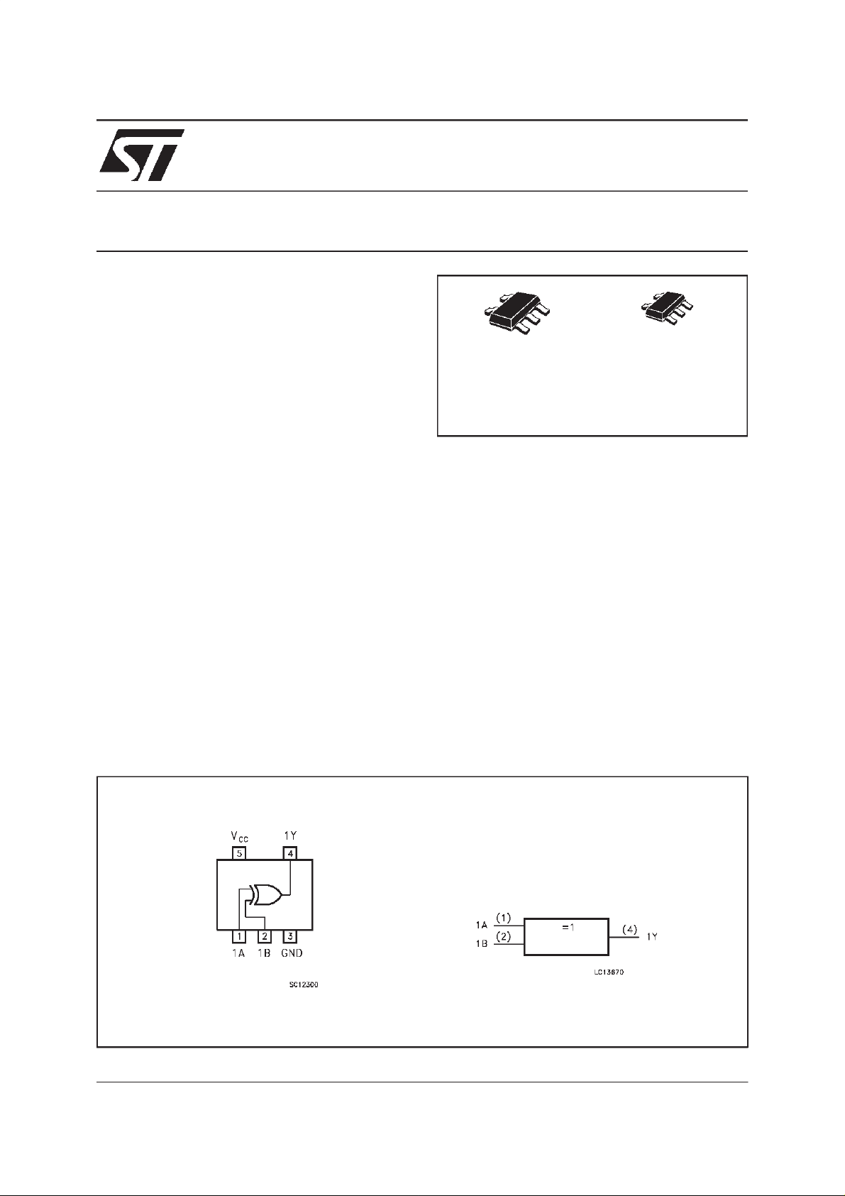
(SOT23-5L)
C
(SC-70)
ORDERCODE:
74V1T86S 74V1T86C
2
wiringC
MOS technology.
Power down protection is provided on all inputs
and 0 to 7V can be accepted on inputs with no
regard to the supply voltage. This device can be
used to interface 5V to 3V.
PIN CONNECTION AND IEC LOGICSYMBOLS
October 1999
1/7
Page 2
74V1T86
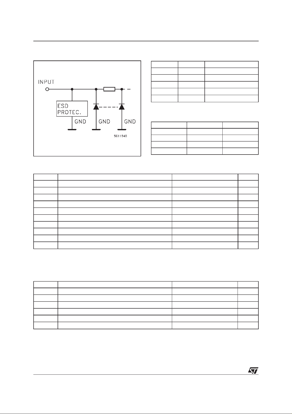
INPUT EQUIVALENTCIRCUIT
PIN DESCRIPTION
PI N No SYMB OL NAME AND FUNCTI ON
1 1A Data Input
2 1B Data Input
4 1Y Data Output
3 GND Ground (0V)
5V
CC
Positive Supply Voltage
TRUTH TABLE
ABY
LLL
LHH
HLH
HHL
ABSOLUTE MAXIMUM RATINGS
Symb o l Para met er Val u e Uni t
V
V
V
V
I
I
OK
I
or I
I
CC
T
T
AbsoluteMaximum Ratingsarethosevaluesbeyond whichdamagetothedevicemayoccur. Functionaloperationunderthese condition isnotimplied.
1)V
=0V
CC
2)HighorLowState
Supply Voltage -0.5 to +7.0 V
CC
DC Input Voltage -0.5 to +7.0 V
I
DC Output Voltage (see note 1) -0.5 to +7.0 V
O
DC Output Voltage (see note 2) -0.5 to VCC+ 0.5 V
O
DC Input Diode Current - 20 mA
IK
DC Output Diode Current ± 20 mA
DC Output Current ± 25 mA
O
DC VCCor Ground Current ± 50 mA
GND
Storage Temperature -65 to +150
stg
Lead Temperature (10 sec) 260
L
o
C
o
C
RECOMMENDEDOPERATING CONDITIONS
Symb o l Para met er Value Un it
V
V
V
V
T
dt/dv Input Rise and Fall Time (see note 3) (V
1)VCC=0V
2)HighorLowState
from0.8Vto 2 V
3)V
IN
2/7
Supply Voltage 4.5 to 5.5 V
CC
Input Voltage 0 to 5.5 V
I
Output Voltage (see note 1) 0 to 5.5 V
O
Output Voltage (see note 2) 0 to V
O
Operating Temperature -40 to +85
op
=5.0±0.5V) 0 to 20 ns/V
CC
CC
V
o
C
Page 3

74V1T86
DC SPECIFICATIONS
Symb o l Para met er Test Co n ditio ns Val u e Uni t
=25oC -40 to 85oC
T
A
Min. Typ. Max. Min. Max.
0.1
±
1.0
±
1.35 1.5 mA
µ
V
V
V
V
I
∆
I
OPD
V
CC
(V)
High Level Input
IH
4.5 to 5.5 2 2 V
Voltage
Low Level Input
IL
4.5 to 5.5 0.8 0.8 V
Voltage
High Level Output
OH
Voltage
Low Level Output
OL
Voltage
Input Leakage Current 0 to 5.5 VI= 5.5V or GND
I
I
Quiescent Supply
CC
4.5 IO=-50 µA 4.4 4.5 4.4
4.5 I
4.5 IO=50 µA 0.0 0.1 0.1
4.5 I
5.5 VI=VCCorGND 1 10 µA
Current
Additional Worst Case
I
CC
Supply Current
Output Leakage
5.5 One Input at 3.4V,
other input at V
0V
Current
=-8 mA 3.94 3.8
O
=8 mA 0.36 0.44
O
or
CC
GND
= 5.5V 0 0.5 5.0 µA
OUT
V
V
A
AC ELECTRICAL CHARACTERISTICS
(Inputt
r=tf
=3 ns)
Symbol Parameter Test Condition Value Unit
t
Propagation Delay
PLH
t
Time
PHL
(*)Voltagerangeis5V± 0.5V
V
(*)
CC
(V)
C
(pF)
L
5.0 15 5.0 7.9 1.0 9.0
5.0 50 5.5 7.9 1.0 9.0
T
=25oC -40 to 85oC
A
Min. Typ. Max. Min. Max.
ns
CAPACITIVE CHARACTERISTICS
Symb o l Para met er Test Co n ditio ns Val u e Uni t
=25oC -40 to 85oC
T
A
Min. Typ. Max. Min. Max.
Input Capacitance 4 10 10
C
IN
Power Dissipation
C
PD
18 pF
Capacitance (note 1)
1)CPDisdefinedasthevalueoftheIC’sinternalequivalent capacitance whichis calculated fromtheoperating currentconsumption withoutload.(Referto
TestCircuit).Averageoperatingcurrentcanbeobtainedbythefollowingequation.I
(opr)=CPD• VCC•fIN+I
CC
CC
pF
3/7
Page 4

74V1T86
TESTCIRCUIT
CL= 15/50 pF or equivalent (includes jig and probe capacitance)
R
ofpulsegenerator(typically50Ω)
T=ZOUT
WAVEFORM:PROPAGATION DELAYS
(f=1MHz;50% duty cycle)
4/7
Page 5

SOT23-5L MECHANICAL DATA
74V1T86
DIM.
MIN. TYP. MAX. MIN. TYP. MAX.
A 0.90 1.45 35.4 57.1
A1 0.00 0.15 0.0 5.9
A2 0.90 1.30 35.4 51.2
b 0.35 0.50 13.7 19.7
C 0.09 0.20 3.5 7.8
D 2.80 3.00 110.2 118.1
E 2.60 3.00 102.3 118.1
E1 1.50 1.75 59.0 68.8
L 0.35 0.55 13.7 21.6
e 0.95 37.4
e1 1.9 74.8
mm mils
5/7
Page 6

74V1T86
SC-70 MECHANICAL DATA
DIM.
MIN. TYP. MAX. MIN. TYP. MAX.
A 0.80 1.10 31.5 43.3
A1 0.00 0.10 0.0 3.9
A2 0.80 1.00 31.5 39.4
b 0.15 0.30 5.9 11.8
C 0.10 0.18 3.9 7.1
D 1.80 2.20 70.9 86.6
E 1.80 2.40 70.9 94.5
E1 1.15 1.35 45.3 53.1
L 0.10 0.30 3.9 11.8
e 0.65 25.6
e1 1.3 51.2
mm mils
6/7
Page 7

74V1T86
Information furnished isbelieved to beaccurate and reliable. However, STMicroelectronics assumes no responsibility for the consequences
of use of such information nor for any infringement of patents or other rights of third parties which may result from its use. No license is
granted by implication or otherwise under any patent or patent rights of STMicroelectronics. Specification mentioned in this publication are
subject to change withoutnotice. Thispublication supersedes and replaces all information previously supplied. STMicroelectronics products
are not authorized for use as critical components in lifesupport devices or systems withoutexpress written approval of STMicroelectronics.
The ST logo is a registeredtrademark of STMicroelectronics
1999 STMicroelectronics – Printed in Italy – All RightsReserved
STMicroelectronics GROUP OF COMPANIES
Australia - Brazil - China- Finland - France -Germany - Hong Kong - India- Italy- Japan- Malaysia - Malta -Morocco
Singapore - Spain- Sweden - Switzerland - United Kingdom - U.S.A.
http://www.st.com
.
7/7
 Loading...