

Page 1
74V1T32
SINGLE 2-INPUT OR GATE
■ HIGHSPEED:t
■ LOW POWERDISSIPAT ION:
=1 µA (MAX.) at TA=25oC
I
CC
■ COMPATIBLEWITHTTLOUTPUTS:
V
=2V(MIN),VIL=0.8V(MAX)
IH
■ POWERDOWN PROTECTIONON INPUTS&
=5 ns(TYP.)atVCC=5V
PD
OUTPUT
■ SYMMETRICALOUTPUT IMPEDANCE:
|I
|=IOL=8 mA(MIN)
OH
■ BALANCEDPROPAGATIONDELAYS:
t
≅ t
PLH
PHL
■ OPERATINGVOLTAGERANGE:
(OPR)= 4.5Vto 5.5V
V
CC
■ IMPROVEDLATCH-UP IMMUNITY
DESCRIPTION
The 74V1T32 is an advancedhigh-speed CMOS
SINGLE 2-INPUT OR GATE fabricated with
sub-micron silicon gate and double-layer metal
wiringC
2
MOStechnology.
S
(SOT23-5L)
C
(SC-70)
ORDERCODE:
74V1T32S 74V1T32C
The internal circuit is composed of 2 stages
including buffer output, which provide high noise
immunityand stableoutput.
Power down protection is provided on all inputs
and 0 to 7V can be accepted on inputs with no
regard to the supply voltage. This device can be
used to interface 5V to 3V.
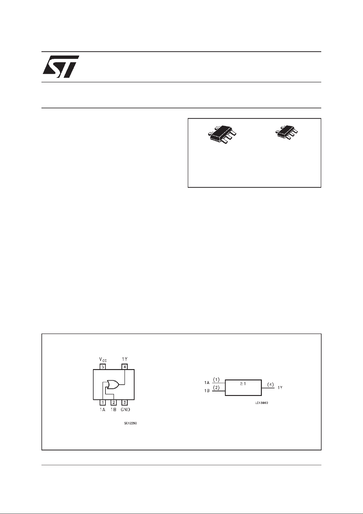
PIN CONNECTION AND IEC LOGIC SYMBOLS
October 1999
1/7
Page 2
74V1T32
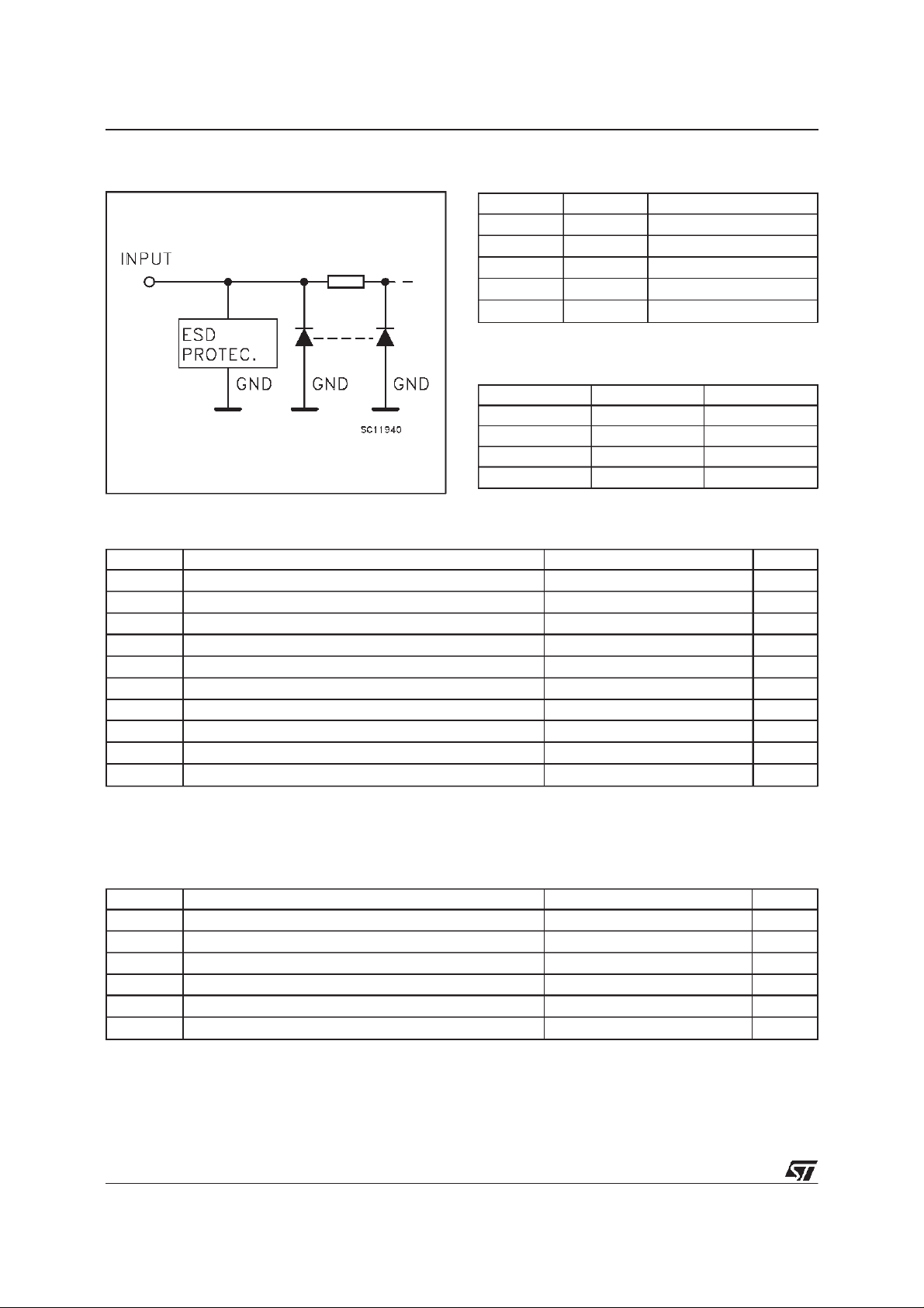
INPUT EQUIVALENTCIRCUIT
PIN DESCRIPTION
PI N No SYMB OL NAME AND FUNCTION
1 1A Data Input
2 1B Data Input
4 1Y Data Output
5 GND Ground (0V)
3V
CC
Positive Supply Voltage
TRUTH TABLE
ABY
LLL
LHH
HLH
HHH
ABSOLUTE MAXIMUM RATINGS
Symb o l Para met er Val u e Uni t
V
V
V
V
I
I
OK
I
or I
I
CC
T
T
AbsoluteMaximumRatingsarethosevaluesbeyondwhichdamagetothedevicemayoccur. Functional operation underthese conditionisnot implied.
1)V
=0V
CC
2)HighorLowState
Supply Voltage -0.5 to +7.0 V
CC
DC Input Voltage -0.5 to +7.0 V
I
DC Output Voltage (see note 1) -0.5 to +7.0 V
O
DC Output Voltage (see note 2) -0.5 to VCC+ 0.5 V
O
DC Input Diode Current - 20 mA
IK
DC Output Diode Current ± 20 mA
DC Output Current ± 25 mA
O
DC VCCor Ground Current ± 50 mA
GND
Storage Temperature -65 to +150
stg
Lead Temperature (10 sec) 260
L
o
C
o
C
RECOMMENDED OPERATINGCONDITIONS
Symb o l Para met er Value Un it
V
V
V
V
T
dt/dv Input Rise and Fall Time (see note 3) (V
1)VCC=0V
2)HighorLowState
from0.8Vto 2 V
3)V
IN
2/7
Supply Voltage 4.5 to 5.5 V
CC
Input Voltage 0 to 5.5 V
I
Output Voltage (see note 1) 0 to 5.5 V
O
Output Voltage (see note 2) 0 to V
O
Operating Temperature -40 to +85
op
=5.0±0.5V) 0 to 20 ns/V
CC
CC
V
o
C
Page 3
74V1T32
DC SPECIFICATIONS
Symb o l Para met er Test Conditio ns Val u e Uni t
=25oC -40 t o 85oC
T
A
Min. Typ. Max. Min. Max.
0.1
±
1.0
±
1.35 1.5 mA
µ
V
V
V
V
I
∆
I
OPD
V
CC
(V)
High Level Input
IH
4.5 to 5.5 2 2 V
Voltage
Low Level Input
IL
4.5 to 5.5 0.8 0.8 V
Voltage
High Level Output
OH
Voltage
Low Level Output
OL
Voltage
Input Leakage Current 0 to 5.5 VI= 5.5V or GND
I
I
Quiescent Supply
CC
4.5 IO=-50 µA 4.4 4.5 4.4
4.5 I
4.5 IO=50 µA 0.0 0.1 0.1
4.5 I
5.5 VI=VCCorGND 1 10 µA
Current
Additional Worst Case
I
CC
Supply Current
Output Leakage
5.5 One Input at 3.4V,
other input at V
0V
Current
=-8 mA 3.94 3.8
O
=8 mA 0.36 0.44
O
or
CC
GND
= 5.5V 0 0.5 5.0 µA
OUT
V
V
A
AC ELECTRICAL CHARACTERISTICS (Inputtr=tf=3 ns)
Symbol Parameter Test Conditi on Value Unit
t
Propagation Delay
PLH
t
Time
PHL
(*)Voltagerangeis5V ±0.5V
V
(*)
CC
(V)
C
(pF)
L
5.0 15 5.0 7.0 1.0 8.0
5.0 50 5.5 8.0 1.0 9.0
T
=25oC -40 t o 85oC
A
Min. Typ. Max. Min. Max.
ns
CAPACITIVE CHARACTERISTICS
Symb o l Para met er Test Conditio ns Val u e Uni t
=25oC -40 t o 85oC
T
A
Min. Typ. Max. Min. Max.
Input Capacitance 4 10 10
C
IN
Power Dissipation
C
PD
12 pF
Capacitance (note 1)
1)CPDisdefined asthevalue oftheIC’sinternal equivalentcapacitance whichiscalculatedfromtheoperatingcurrentconsumption withoutload.(Referto
TestCircuit).Average operatingcurrent canbeobtained bythefollowingequation.I
(opr)= CPD• VCC•fIN+I
CC
CC
pF
3/7
Page 4

74V1T32
TESTCIRCUIT
CL= 15/50pFor equivalent (includes jigand probe capacitance)
R
ofpulsegenerator (typically50Ω)
T=ZOUT
WAVEFORM:PROPAGATIONDELAYS
(f=1MHz;50% duty cycle)
4/7
Page 5

SOT23-5L MECHANICAL DATA
74V1T32
DIM.
MIN. TYP. MAX. MIN. TYP. MAX.
A 0.90 1.45 35.4 57.1
A1 0.00 0.15 0.0 5.9
A2 0.90 1.30 35.4 51.2
b 0.35 0.50 13.7 19.7
C 0.09 0.20 3.5 7.8
D 2.80 3.00 110.2 118.1
E 2.60 3.00 102.3 118.1
E1 1.50 1.75 59.0 68.8
L 0.35 0.55 13.7 21.6
e 0.95 37.4
e1 1.9 74.8
mm mils
5/7
Page 6

74V1T32
SC-70 MECHANICAL DATA
DIM.
MIN. TYP. MAX. MIN. TYP. MAX.
A 0.80 1.10 31.5 43.3
A1 0.00 0.10 0.0 3.9
A2 0.80 1.00 31.5 39.4
b 0.15 0.30 5.9 11.8
C 0.10 0.18 3.9 7.1
D 1.80 2.20 70.9 86.6
E 1.80 2.40 70.9 94.5
E1 1.15 1.35 45.3 53.1
L 0.10 0.30 3.9 11.8
e 0.65 25.6
e1 1.3 51.2
mm mils
6/7
Page 7

74V1T32
Information furnished isbelieved tobe accurate andreliable. However, STMicroelectronicsassumes no responsibility forthe consequences
of use of such information nor for any infringement of patents or other rights of third parties which may result from its use. No license is
granted by implication or otherwise under any patent or patent rights of STMicroelectronics. Specification mentioned in this publication are
subject to change without notice. Thispublication supersedes andreplaces all information previously supplied. STMicroelectronics products
are not authorized for use as critical components in lifesupport devices or systems withoutexpress written approval of STMicroelectronics.
The ST logo isa registeredtrademark of STMicroelectronics
1999 STMicroelectronics – Printed in Italy– All Rights Reserved
STMicroelectronics GROUP OF COMPANIES
Australia - Brazil- China- Finland - France -Germany - Hong Kong - India - Italy - Japan- Malaysia - Malta - Morocco
Singapore - Spain- Sweden - Switzerland - United Kingdom - U.S.A.
http://www.st.com
.
7/7
 Loading...