

Page 1
74V1T125
SINGLE BUS BUFFER (3-STATE)
■ HIGH SPEED: t
■ LOW POWER DISSIPATION:
I
=1µA(MAX.) at TA=25°C
CC
■ COMPATIBLE WITHTTL OUTPUTS:
V
=2V(MIN),VIL=0.8V(MAX)
IH
■ POWER DOWN PROTECTION ON INPUTS
■ SYMMETRICAL OUTPUTIMPEDANCE:
|I
|=IOL=8mA(MIN)atVCC=4.5V
OH
■ BALANCED PROPAGATION DELAYS:
t
≅ t
PLH
PHL
■ OPERATING VOLTAGE RANGE:
V
(OPR) = 4.5V to 5.5V
CC
= 3.5ns (TYP.) at VCC=5V
PD
DESCRIPTION
The 74V1T125 is an advanced high-speed CM OS
SINGLE BUS BUFFER fabricatedwith sub-micron
silicon gate and double-layer me tal wiring C
2
MOS
technology.
3-STATE control input G
has to be set HIGH t o
place the out put into the high impedance state.
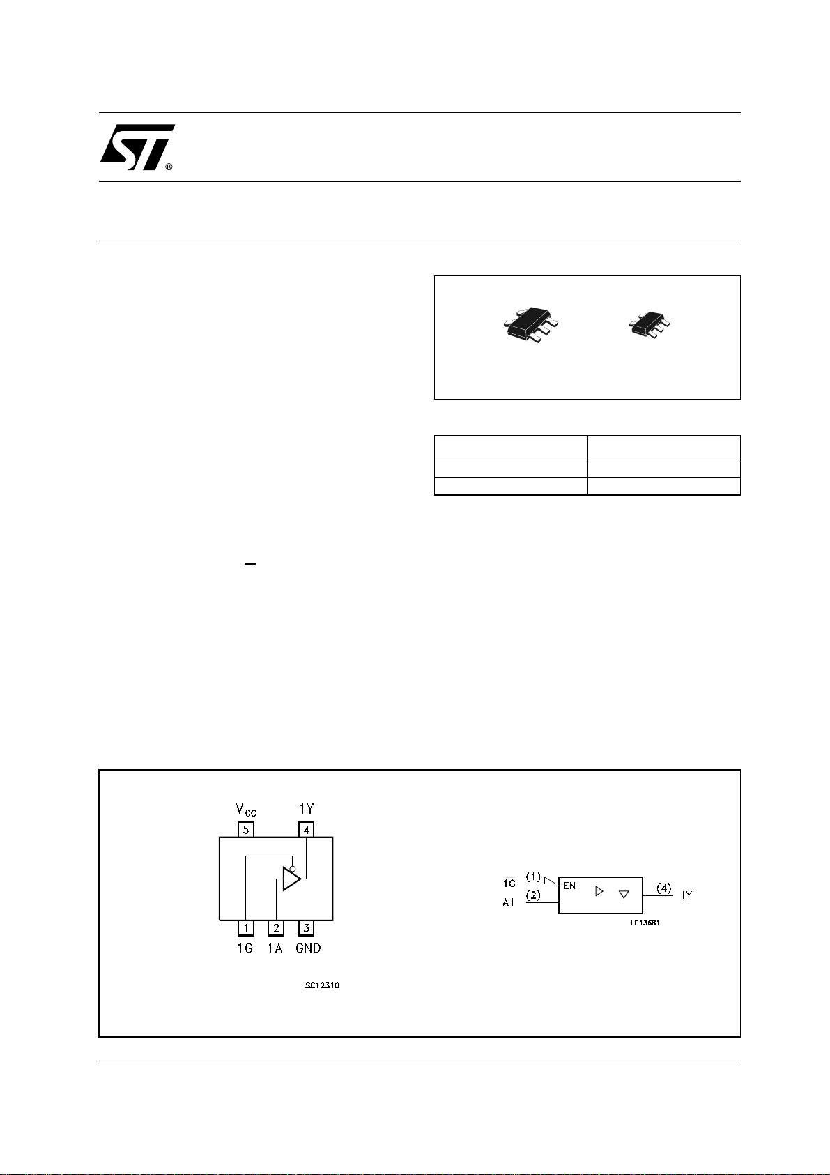
SOT323-5LSOT23-5L
ORDER CODES
PACKAGE T & R
SOT23-5L 74V1T125STR
SOT323-5L 74V1T125CTR
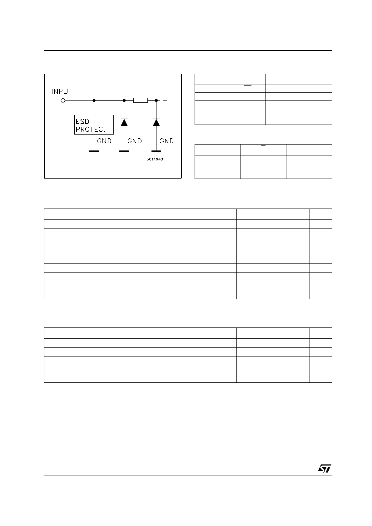
Power down protection is provided on all inputs
and 0 to 7V can be accepted on inputs with no
regard to the supply voltage. This device can be
usedto interface 5V to 3V.
PIN CONNECTION AND IEC LOGIC SYMBOLS
1/10April 2004
Page 2
74V1T125
INPUT EQUIVALENT CIRCUIT PIN DESCRIPTION
PIN N° SYMBOL NAME AND FUNCTION
11G
2 1A Data Input
4 1Y Data Output
3 GND Ground (0V)
5
TRUTH TABLE
V
CC
Output Enable Input
Positive Supply Voltage
AG
Y
XHZ
LLL
HLH
X : Don’t Care
Z : High Impedance
ABSOLUTE MAXIMUM RATINGS
Symbol Parameter Value Unit
V
V
V
I
I
OK
I
I
or I
CC
T
T
Absolute Maximum Ratings are those values beyond which damage to the device may occur. Functional operation under these conditions is
not implied
Supply Voltage
CC
DC Input Voltage
I
DC Output Voltage -0.5 to VCC+0.5
O
DC Input Diode Current
IK
DC Output Diode Current
DC Output Current
O
DC VCCor Ground Current
GND
Storage Temperature
stg
Lead Temperature (10 sec)
L
-0.5 to +7.0 V
-0.5 to +7.0 V
V
-20 mA
± 20 mA
± 25 mA
± 50 mA
-65 to +150 °C
300 °C
RECOMMENDED OPERATING CONDITIONS
Symbol Parameter Value Unit
V
V
V
T
dt/dv
1) VINfrom0.8V to 2V
Supply Voltage
CC
Input Voltage
I
Output Voltage 0 to V
O
Operating Temperature
op
Input Rise and Fall Time (note 1) (V
=5.0± 0.5V)
CC
4.5 to 5.5 V
0to5.5 V
CC
-55 to 125 °C
0 to 20 ns/V
2/10
V
Page 3
DC SPECIFICATIONS
Symbol Parameter
V
V
V
+I
High Level Input
IH
Voltage
V
Low Level Input
IL
Voltage
High Level Output
OH
Voltage
Low Level Output
OL
Voltage
I
High Impedance
OZ
Output Leakage
Current
Input Leakage
I
I
Current
I
Quiescent Supply
CC
Current
Additional Worst
CC
Case Supply
Current
Test Condition Value
T
= 25°C
V
CC
(V)
4.5to
A
Min. Typ. Max. Min. Max. Min. Max.
222V
5.5
4.5to
5.5
4.5
4.5
4.5
4.5
5.5
0to
5.5
5.5
IO=-50 µA 4.4 4.5 4.4 4.4 V
=-8 mA 3.94 3.8 3.7
I
O
IO=50 µA 0.0 0.1 0.1 0.1 V
I
=8 mA 0.36 0.44 0.55
O
I=VIH
or V
IL
V
VO=VCCor GND
V
=5.5VorGND
I
V
I=VCC
or GND
One Input at 3.4V,
other input at V
5.5
CC
or GND
74V1T125
-40 to 85°C -55 to 125°C
0.8 0.8 0.8 V
±0.25 ± 2.5 ± 5.0 µA
± 0.1 ± 1.0 ± 1.0 µA
11020µA
1.35 1.5 1.5 mA
Unit
AC ELECTRICAL CHARACTERISTICS (Input t
Test Condition Value
Symbol Parameter
t
t
t
t
t
t
(*) Voltage range is 5.0V± 0.5V
Propagation Delay
PLH
Time
PHL
Output Disable
PLZ
Time
PHZ
Output Enable
PZL
Time
PZH
V
(V)
5.0
5.0
5.0
5.0
5.0
5.0
C
CC
L
(pF)
(*)
15 3.5 6.0 1.0 7.0 1.0 8.0
(*)
50 3.8 6.5 1.0 7.5 1.0 8.5
(*)
15 3.9 5.0 1.0 6.0 1.0 7.0
(*)
50 4.3 7.0 1.0 8.0 1.0 9.0
(*)
15 4.3 7.0 1.0 8.0 1.0 9.0
(*)
50 4.7 7.5 1.0 8.5 1.0 9.5
=3ns)
r=tf
= 25°C
T
A
-40 to 85°C -55 to 125°C
Min. Typ. Max. Min. Max. Min. Max.
Unit
ns
ns
ns
3/10
Page 4

74V1T125
CAPACITIVE CHARACTERISTICS
Test Condition Value
= 25°C
Symbol Parameter
T
A
Min. Typ. Max. Min. Max. Min. Max.
C
C
C
Input Capacitance
IN
Output
OUT
Capacitance
Power Dissipation
PD
Capacitance
410 10 10pF
5pF
14 pF
(note 1)
1) CPDis defined as the value of the IC’s internal equivalent capacitance which is calculated from the operating current consumption without
load. (Refer to Test Circuit). Average operating current can be obtained by the following equation. I
TEST CIRCUIT
-40 to 85°C -55 to 125°C
CC(opr)=CPDxVCCxfIN+ICC
Unit
TEST SWITCH
t
PLH,tPHL
t
PZL,tPLZ
t
PZH,tPHZ
CL=15/50pF or equivalent (includes jig and probe capacitance)
R1 = 1KΩ or equivalent
R
T=ZOUT
of pulse generator (typically 50Ω)
4/10
Open
V
CC
GND
Page 5

WAVEFORM 1: PROPAG ATION DELAYS (f=1MHz; 50% duty cycle)
WAVEFORM 2: O UTPUT E NABLE AND DISABLE TIME (f=1MHz; 50% duty cycle)
74V1T125
5/10
Page 6

74V1T125
SOT23-5L MECHANICAL DATA
mm. mils
DIM.
MIN. TYP MAX. MIN. TYP. MAX.
A 0.90 1.45 35.4 57.1
A1 0.00 0.10 0.0 3.9
A2 0.90 1.30 35.4 51.2
b 0.35 0.50 13.7 19.7
C 0.09 0.20 3.5 7.8
D 2.80 3.00 110.2 118.1
E 1.50 1.75 59.0 68.8
e0.95 37.4
H 2.60 3.00 102.3 118.1
L 0.10 0.60 3.9 23.6
.
6/10
7049676C
Page 7

74V1T125
SOT323-5L MECHANICAL DATA
mm. mils
DIM.
MIN. TYP MAX. MIN. TYP. MAX.
A 0.80 1.10 31.5 43.3
A1 0.00 0.10 0.0 3.9
A2 0.80 1.00 31.5 39.4
b 0.15 0.30 5.9 11.8
C 0.10 0.18 3.9 7.1
D 1.80 2.20 70.9 86.6
E 1.80 2.40 70.9 94.5
E1 1.15 1.35 45.3 53.1
e
e1 1.3 51.2
L 0.10 0.30 3.9 11.8
.65
0
25.6
7/10
Page 8

74V1T125
Tape & Reel SOT23-xL MECHANICAL D ATA
DIM.
MIN. TYP MAX. MIN. TYP. MAX.
A 180 7.086
C 12.8 13.0 13.2 0.504 0.512 0.519
D 20.2 0.795
N 60 2.362
T 14.4 0.567
Ao 3.13 3.23 3.33 0.123 0.127 0.131
Bo 3.07 3.17 3.27 0.120 0.124 0.128
Ko 1.27 1.37 1.47 0.050 0.054 0.0.58
Po 3.9 4.0 4.1 0.153 0.157 0.161
P 3.9 4.0 4.1 0.153 0.157 0.161
mm. inch
8/10
Page 9

Tape & Reel SOT323-xL MECHANICAL DATA
74V1T125
DIM.
MIN. TYP MAX. MIN. TYP. MAX.
A 175 180 185 6.889 7.086 7.283
C 12.8 13 13.2 0.504 0.512 0.519
D 20.2 0.795
N 59.5 60 60.5 2.362
T 14.4 0.567
Ao 2.25 0.088
Bo 2.7 0.106
Ko 1.2 0.047
Po 3.9 4 4.1 0.153 0.157 0.161
P 3.8 4 4.2 0.149 0.157 0.165
mm. inch
9/10
Page 10

74V1T125
Information furnished is believed to be accurate and reliable. However, STMicroelectronics assumes no responsibility for the
consequences of use of such inform ation nor fo r an y infring ement of p atents or o ther rights of third p arties which may r esult f rom
its use. No license is granted by implication or otherwise under any patent or patent rights of STMicroelectronics. Specifications
mentioned in this publication are subject to change without notice. This publication supersedes and replaces all information
previously supplied. STMicroelectronics products ar e not authorized for use as critical components in life support devices or
systems without express written approval of STMicroelectronics.
Australia - Belgium - Brazil - Canada - China - Czech Republic - Finland - France - Germany - Hong Kong - India - Israel - Italy - Japan -
Malaysia - Malta - Morocco - Singapore - Spain - Sweden - Switzerland - United Kingdom - United States.
The ST logo is a registered trademark of STMicroelectronics
All other names are the property of their respective owners
© 2004 STMicroelectronics - All Rights Reserved
STMicroelectronics GROUP OF COMPANIES
http://www.st.com
10/10
 Loading...