

Page 1
SINGLE INVERTER(OPEN DRAIN)
■ HIGHSPEED:t
■ LOW POWER DISSIPATION:
=1 µA (MAX.)at TA=25oC
I
CC
■ COMPATIBLEWITHTTLOUTPUTS:
=2V(MIN),VIL=0.8V(MAX)
V
IH
■ POWERDOWNPROTECTIONON INPUTS
■ OPERATINGVOLTAGERANGE:
(OPR)= 4.5Vto 5.5V
V
CC
■ IMPROVEDLATCH-UPIMMUNITY
=6ns (TYP.)atVCC=5V
PD
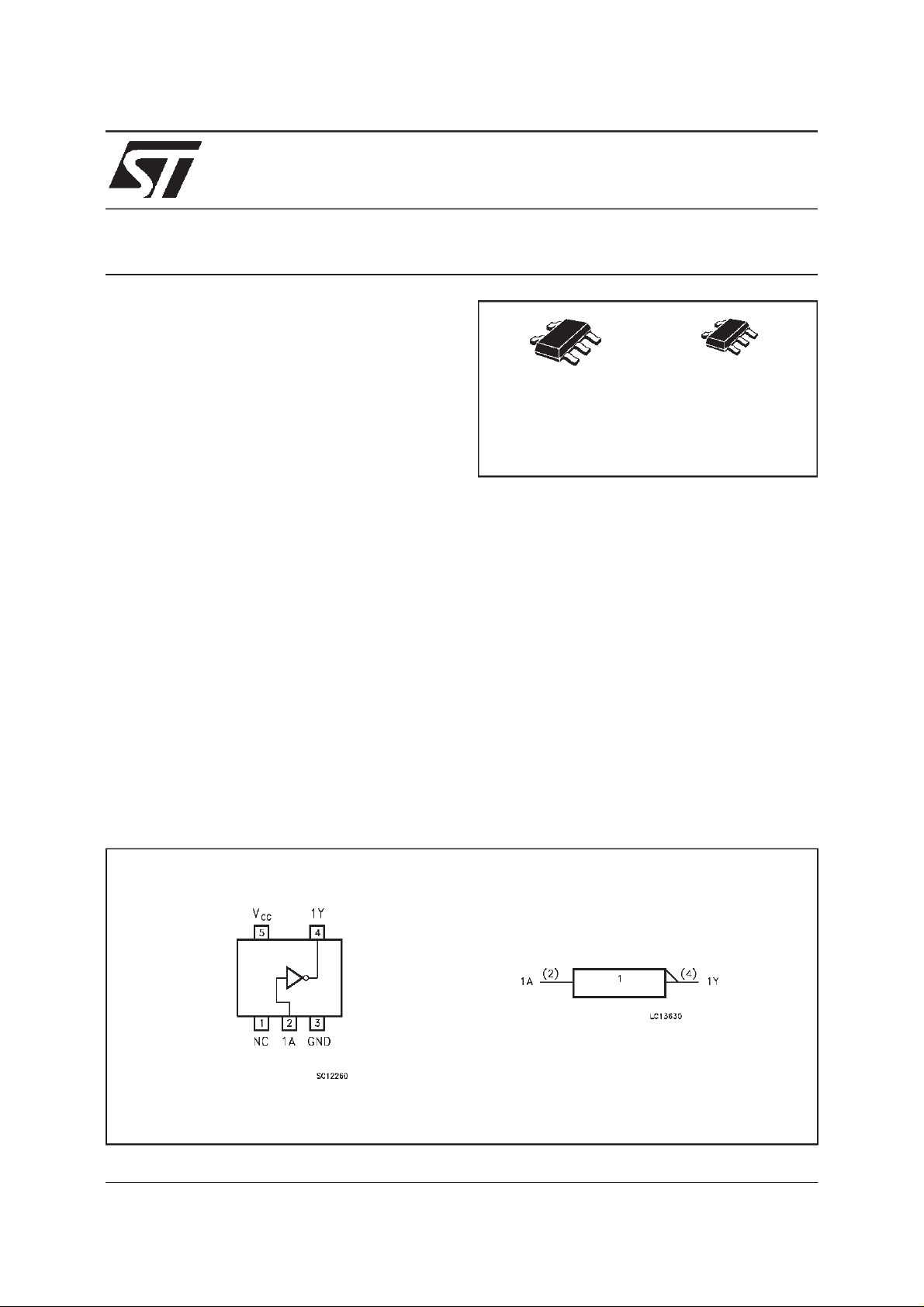
74V1T05
PRELIMINARY DATA
S
(SOT23-5L)
ORDERCODE:
74V1T05S 74V1T05C
C
(SC-70)
DESCRIPTION
The 74V1T05 is an advanced high-speed CMOS
SINGLE INVERTER (OPEN DRAIN) fabricated
with sub-micron silicon gate and double-layer
metalwiring C
2
MOStechnology.
The internal circuit is composed of 3 stages
including buffer output, which provide high noise
immunityand stableoutput.
PIN CONNECTION AND IEC LOGICSYMBOLS
This device can, with an external pull-up resistor,
be used in wired AND configuration. This device
can also be used as a led driver in any other
applicationrequiring a currentsink.
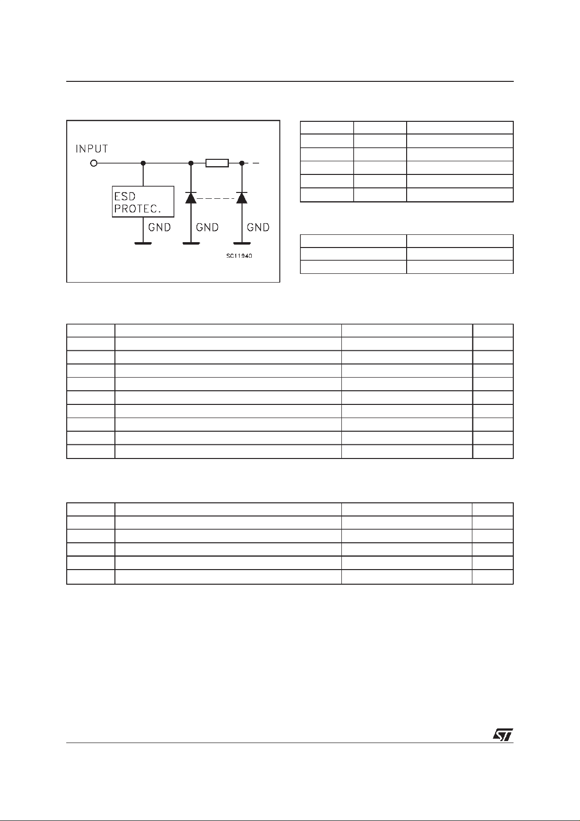
Power down protection is provided on inputand 0
to 7V can be accepted on inputwith no regard to
the supply voltage. This device can be used to
interface5V to 3V.
September 1999
1/7
Page 2
74V1T05
INPUT EQUIVALENTCIRCUIT
PIN DESCRIPTION
PI N No SYMB OL NAME AND F U NCTIO N
1 N.C. Not Connected
2 1A Data Input
4 1Y Data Output
3 GND Ground (0V)
5V
CC
Positive Supply Voltage
TRUTH TABLE
AY
LZ
HL
Z: High Impedance
ABSOLUTE MAXIMUM RATINGS
Symb o l Para met er Val u e Uni t
V
V
V
I
I
OK
I
or I
I
CC
T
T
AbsoluteMaximumRatingsarethosevaluesbeyondwhichdamageto thedevicemayoccur.Functionaloperationunderthesecondition isnotimplied.
Supply Voltage -0.5 to +7.0 V
CC
DC Input Voltage -0.5 to +7.0 V
I
DC Output Voltage -0.5 to VCC+ 0.5 V
O
DC Input Diode Current - 20 mA
IK
DC Output Diode Current
DC Output Current 25 mA
O
DC VCCor Ground Current ± 50 mA
GND
Storage Temperature -65 to +150
stg
Lead Temperature (10 sec) 260
L
20 mA
±
o
C
o
C
RECOMMENDED OPERATINGCONDITIONS
Symb o l Para met er Value Un it
V
V
V
T
dt/dv
1) VINfrom0.8Vto2 V
2/7
Supply Voltage 4.5 to 5.5 V
CC
Input Voltage 0 to 5.5 V
I
Output Voltage 0 to V
O
Operating Temperature -40 to +85
op
Input Rise and Fall Time (see note 1) (V
=5.0±0.5V)
CC
CC
0 to 20 ns/V
V
o
C
Page 3
74V1T05
DC SPECIFICATIONS
Symb o l Para met er Test Con diti o ns Val u e Uni t
T
V
CC
High Level Input
V
IH
(V)
4.5 to 5.5 2 2 V
Min. Typ. Max. Min. Max.
Voltage
V
IL
Low Level Input
4.5 to 5.5 0.8 0.8 V
Voltage
Low Level Output
V
OL
Voltage
High Impedance
I
OZ
Output Leakage
4.5 IO=50 µ A 0.0 0.1 0.1
4.5 I
5.5
=8 mA 0.36 0.44
O
VI=VIHor V
IL
VO=VCCor GND
Current
Input Leakage Current 0 to 5.5 VI= 5.5V or GND
I
I
Quiescent Supply
I
CC
5.5 VI=VCCorGND 1 10 µA
Current
Additional Worst Case
I
∆
CC
Supply Current
5.5 One Input at 3.4V,
other input at V
CC
or
GND
=25oC -40 to 85oC
A
0.25
±
0.1
±
1.35 1.5 mA
2.5
±
1.0
±
µ
µ
V
A
A
AC ELECTRICAL CHARACTERISTICS
(Inputt
r=tf
=3 ns)
Symbol Parameter Test Condition Value Unit
V
(*)
t
Propagation Delay
PLz
t
Time
PzL
(*)Voltagerange is5V ± 0.5V
CC
(V)
C
(pF)
L
5.0 15 RL=1K
5.0
50 R
=1KΩ 6.5 8.0 1.0 9.0
L
Min. Typ. Max. Min. Max.
Ω
=25oC -40 to 85oC
T
A
6.0 7.0 1.0 8.0
ns
CAPACITIVE CHARACTERISTICS
Symb o l Para met er Test Con diti o ns Val u e Uni t
=25oC -40 to 85oC
T
A
Min. Typ. Max. Min. Max.
C
Input Capacitance 4 10 10
IN
C
Output Capacitance 5
OUT
Power Dissipation
C
PD
10.5 pF
Capacitance (note 1)
1)CPDisdefined asthevalue oftheIC’sinternal equivalentcapacitance whichiscalculated fromtheoperating currentconsumption without load.(Referto
TestCircuit).Average operatingcurrent canbeobtainedbythefollowingequation.I
(opr)= CPD• VCC• fIN+I
CC
CC
pF
pF
3/7
Page 4

74V1T05
TESTCIRCUIT
CL= 15/50 pF orequ ivalent (includes jigand probe capacitance)
R
=1KΩ orequivalent
L=R1
R
WAVEFORM:PROPAGATIONDELAYS (f=1MHz; 50% duty cycle)
ofpulse generator (typically50Ω)
T=ZOUT
4/7
Page 5

SOT23-5L MECHANICAL DATA
74V1T05
DIM.
MIN. TYP. MAX. MIN. TYP. MAX.
A 0.90 1.45 35.4 57.1
A1 0.00 0.15 0.0 5.9
A2 0.90 1.30 35.4 51.2
b 0.35 0.50 13.7 19.7
C 0.09 0.20 3.5 7.8
D 2.80 3.00 110.2 118.1
E 2.60 3.00 102.3 118.1
E1 1.50 1.75 59.0 68.8
L 0.35 0.55 13.7 21.6
e 0.95 37.4
e1 1.9 74.8
mm mils
5/7
Page 6

74V1T05
SC-70 MECHANICAL DATA
DIM.
MIN. TYP. MAX. MIN. TYP. MAX.
A 0.80 1.10 31.5 43.3
A1 0.00 0.10 0.0 3.9
A2 0.80 1.00 31.5 39.4
b 0.15 0.30 5.9 11.8
C 0.10 0.18 3.9 7.1
D 1.80 2.20 70.9 86.6
E 1.80 2.40 70.9 94.5
E1 1.15 1.35 45.3 53.1
L 0.10 0.30 3.9 11.8
e 0.65 25.6
e1 1.3 51.2
mm mils
6/7
Page 7

74V1T05
Information furnished is believed to beaccurate and reliable. However, STMicroelectronics assumes no responsibility forthe consequences
of use of such information nor for any infringement of patents or other rights of third parties which may result from its use. No license is
granted by implication or otherwise under any patent or patent rights of STMicroelectronics. Specification mentioned in thispublication are
subject tochange without notice. Thispublication supersedes and replaces all information previously supplied. STMicroelectronics products
are not authorized for use as critical components in life support devices or systems without express written approval of STMicroelectronics.
The ST logo is a trademark of STMicroelectronics
1999 STMicroelectronics – Printed in Italy –All Rights Reserved
STMicroelectronics GROUP OF COMPANIES
Australia - Brazil - Canada - China -France -Germany - Italy - Japan -Korea - Malaysia - Malta - Mexico - Morocco -The Netherlands -
Singapore - Spain -Sweden - Switzerland- Taiwan - Thailand - UnitedKingdom -U.S.A.
http://www.st.com
.
7/7
 Loading...