

Page 1
查询74V1G80供应商
74V1G80
SINGLE POSITIVE EDGE TRIGGERED
D-TYPE FLIP-FLOP
■ HIGH SPEED:
f
= 180MHz (TYP.) at VCC = 5V
MAX
■ LOW POWER DISSIPATION:
I
= 1µA(MAX.) at TA=25°C
CC
■ HIGH NOISE IMMUNITY:
V
= V
NIH
■ POWER DOWN PROTECTION ON INPUTS
■ SYMMETRICAL OUTPUT IMPEDANCE:
|I
| = IOL = 8mA (MIN) at VCC = 4.5V
OH
■ BALANCED PROPAGATION DELAYS:
t
≅ t
PLH
■ OPERATING VOL TAGE RANGE:
V
(OPR) = 2V to 5.5V
CC
■ IMPROVED LATCH-UP IMMUNITY
= 28% VCC (MIN.)
NIL
PHL
DESCRIPTION
The 74V1G80 is an advanced high-speed CMOS
SINGLE POSITIVE EDGE TRIGGERED D-TYPE
FLIP-FLOP WITH INVERTED OUTPUT
fabricated with sub-micron silicon gate and
double-layer metal wiring C
2
MOS technology. it is
designed to operate from 2V to 5.5V , making t his
device ideal for portable applications.
This D-Type flip-flop is controlled by a clock input
(CK). On the positive transition of the clock, the Q
output will be set to the logic inverted sta te that
was setup at the D input.
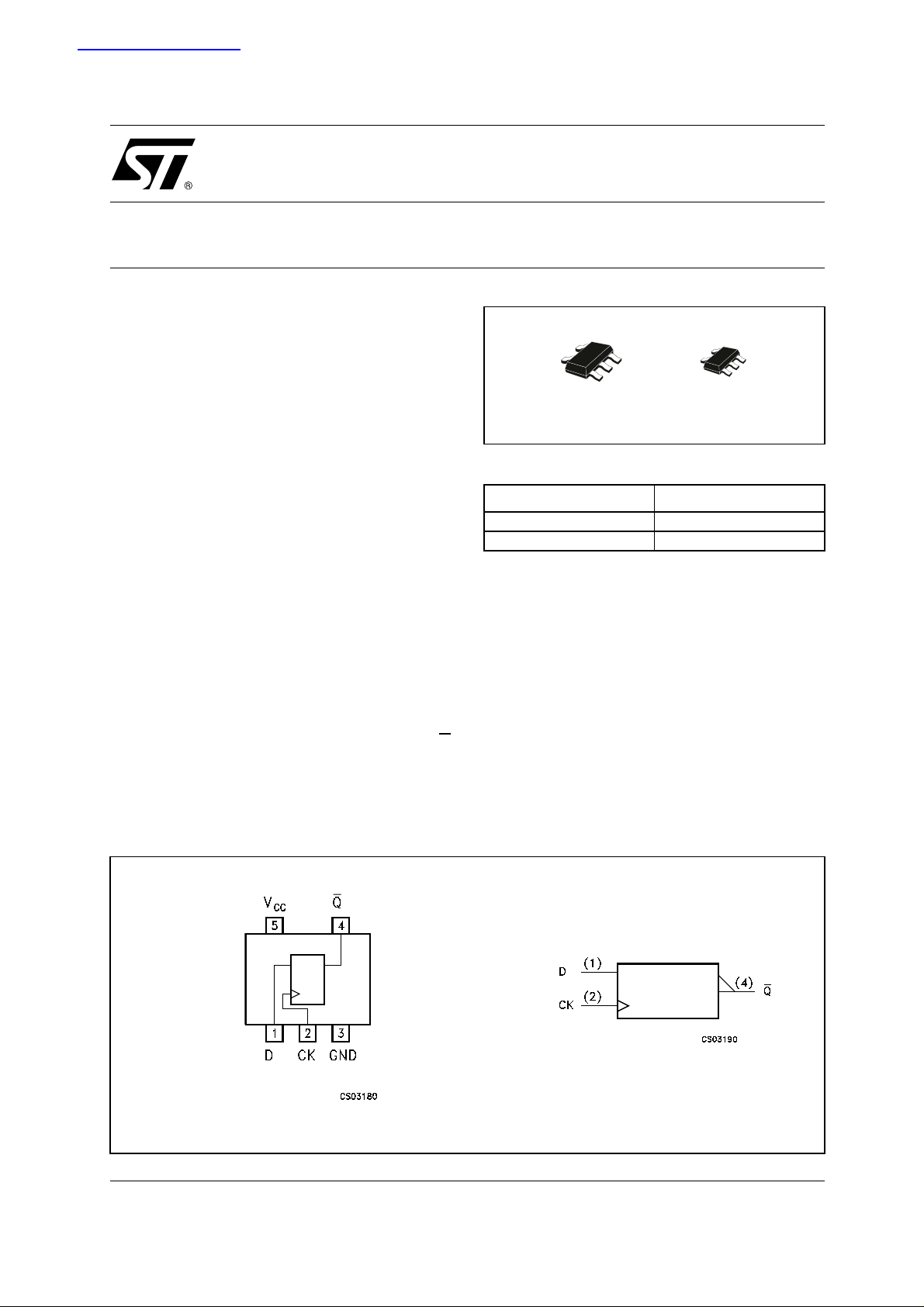
SOT323-5LSOT23-5L
ORDER CODES
PACKAGE T & R
SOT23-5L 74V1G80STR
SOT323-5L 74V1G80CTR
Following the hold time interval, data at the D input
can be changed without affecting the level at the
output. Power down protection is provided on
input and 0 to 7V can be accepted on input with no
regard to the supply voltage. This device can be
used to interface 5V to 3V.
It’s available in the commercial temperature
range. All inputs and output are equipped with
protection circuits against stat ic discharge, giving
them ESD immunity and transient excess voltage.
PIN CONNECTION AND IEC LOGIC SYMBOLS
1/10July 2001
Page 2
74V1G80
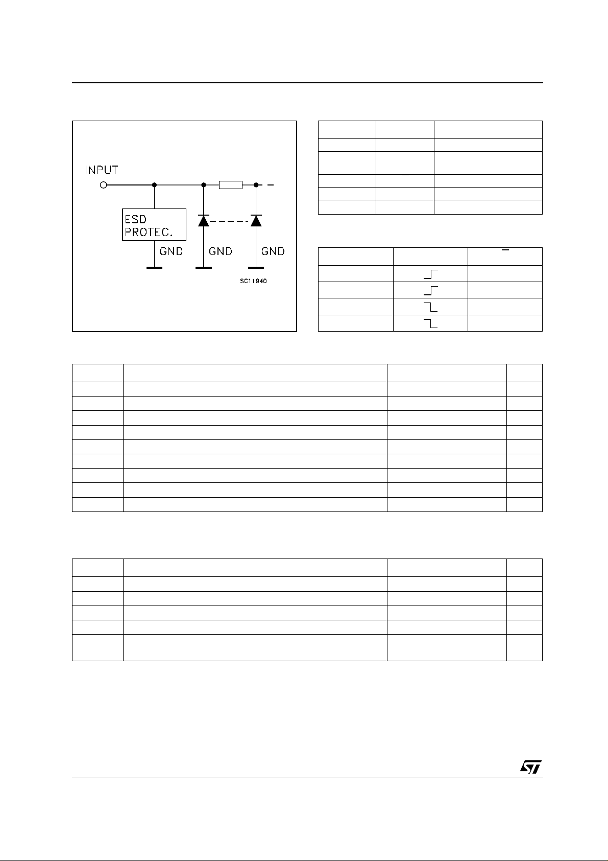
INPUT EQUIVALENT CIRCUIT PIN DESCRIPTION
PIN No SYMBOL NAME AND FUNCTION
1 D Data Input
2CK
4Q
3 GND Ground (0V)
5
TRUTH TABLE
DCKQ
LH
HL
LQn
HQn
ABSOLUTE MAXIMUM RATINGS
V
CC
Clock Input (Positive
Edge)
Inverted Flip-Flop Output
Positive Supply Voltage
Symbol Parameter Value Unit
V
V
V
I
I
OK
I
I
or I
CC
T
T
Absolute Maximum Ratings are those values beyond which damage to the device may occur. Functional operation under these conditions is
not implied.
Supply Voltage
CC
DC Input Voltage
I
DC Output Voltage -0.5 to VCC + 0.5
O
DC Input Diode Current
IK
DC Output Diode Current
DC Output Current
O
DC VCC or Ground Current
GND
Storage Temperature
stg
Lead Temperature (10 sec)
L
-0.5 to +7.0 V
-0.5 to +7.0 V
V
- 20 mA
± 20 mA
± 25 mA
± 50 mA
-65 to +150 °C
260 °C
RECOMMENDED OPERATING CONDITIONS
Symbol Parameter Value Unit
V
V
V
T
dt/dv
1) VIN from 30 % to 70% of V
Supply Voltage
CC
Input Voltage
I
Output Voltage 0 to V
O
Operating Temperature
op
Input Rise and Fall Time (note 1) (V
(V
CC
= 3.3 ± 0.3V)
CC
= 5.0 ± 0.5V)
CC
2 to 5.5 V
0 to 5.5 V
CC
-55 to 125 °C
0 to 100
0 to 20
ns/V
ns/V
V
2/10
Page 3
DC SPECIFICATIONS
Symbol Parameter
V
V
V
V
I
High Level Input
IH
Voltage
Low Level Input
IL
Voltage
High Level Output
OH
Voltage
Low Level Output
OL
Voltage
I
Input Leakage
I
Current
Quiescent Supply
CC
Current
Test Condition Value
V
(V)
CC
= 25°C
A
Min. Typ. Max. Min. Max. Min. Max.
-40 to 85°C -55 to 125°C
T
2.0 1.5 1.5 1.5
3.0 to
5.5
0.7V
CC
0.7V
CC
0.7V
CC
2.0 0.5 0.5 0.5
3.0 to
5.5
2.0
3.0
4.5
3.0
4.5
2.0
3.0
4.5
3.0
4.5
0 to
5.5
5.5
=-50 µA
I
O
I
=-50 µA
O
I
=-50 µA
O
I
=-4 mA
O
I
=-8 mA
O
IO=50 µA
I
=50 µA
O
I
=50 µA
O
I
=4 mA
O
I
=8 mA
O
V
= 5.5V or GND
I
= VCC or GND
V
I
1.9 2.0 1.9 1.9
2.9 3.0 2.9 2.9
4.4 4.5 4.4 4.4
2.58 2.48 2.4
3.94 3.8 3.7
0.3V
CC
0.3V
CC
0.0 0.1 0.1 0.1
0.0 0.1 0.1 0.1
0.0 0.1 0.1 0.1
0.36 0.44 0.55
0.36 0.44 0.55
± 0.1 ± 1 ± 1 µA
11020µA
74V1G80
Unit
0.3V
CC
V
V
V
V
AC ELECTRICAL CHARACTERISTICS (Input t
Test Condition Value
Symbol Parameter
t
PLH tPHL
f
MAX
(*) Vol tage range is 3.3V ± 0.3V
(**) Voltage range is 5.0V ±
Propagation Delay
Time CK to Q
CK Pulse Width,
t
W
HIGH or LOW
Setup Time D to
t
s
CK, HIGH or LOW
Hold Time D to CK,
t
h
HIGH or LOW
Maximum Clock
Frequency
0.5V
3.3
3.3
5.0
5.0
3.3
5.0
3.3
5.0
3.3
5.0
3.3
5.0
C
V
CC
(V)
L
(pF)
(*)
15 4.9 8.4 1.0 9.8 1.0 10.8
(*)
50 5.9 12.0 1.0 14.0 1.0 15.0
(**)
15 3.5 5.6 1.0 7.0 1.0 8.0
(**)
50 4.5 8.0 1.0 10.0 1.0 11.0
(*)
(**)
(*)
(**)
(*)
(**)
(*)
50 100 120 90 90
(**)
50 165 180 150 150
= tf = 3ns)
r
T
= 25°C
A
-40 to 85°C -55 to 125°C
Min. Typ. Max. Min. Max. Min. Max.
4.0 4.0 4.0
3.0 3.0 3.0
4.0 4.0 4.0
3.0 3.0 3.0
1.0 1.0 1.0
1.0 1.0 1.0
Unit
ns
ns
ns
ns
MHz
3/10
Page 4
74V1G80
CAPACITIVE CHARACTERISTICS
Test Condition Value
= 25°C
Symbol Parameter
T
A
Min. Typ. Max. Min. Max. Min. Max.
C
C
Input Capacitance
IN
Power Dissipation
PD
Capacitance
4101010pF
8pF
(note 1)
1) CPD is defined as the value of the IC’s internal equivalent capacitance which is calculated from the operating current consumption without
load. (R ef er to Test Circ ui t). Averag e operating current can be obtained by t he following equation. I
TEST CIRCUIT
-40 to 85°C -55 to 125°C
= CPD x VCC x fIN + I
CC(opr)
CC
Unit
CL = 15/50pF or e qui valent (includes jig and probe capa ci t ance)
R
= Z
of pulse generator (typically 50Ω)
T
OUT
4/10
Page 5

74V1G80
WAVEFORM: PROPAGATION DELAY, SETUP AND HOLD TIM ES (f=1MHz; 50% duty cycl e)
5/10
Page 6

74V1G80
SOT23-5L MECHANICAL DATA
mm. mils
DIM.
MIN. TYP MAX. MIN. TYP. MAX.
A 0.90 1.45 35.4 57.1
A1 0.00 0.15 0.0 5.9
A2 0.90 1.30 35.4 51.2
b 0.35 0.50 13.7 19.7
C 0.09 0.20 3.5 7.8
D 2.80 3.00 110.2 118.1
E 2.60 3.00 102.3 118.1
E1 1.50 1.75 59.0 68.8
e0.95 37.4
e1 1.9 74.8
L 0.35 0.55 13.7 21.6
6/10
Page 7

74V1G80
SOT323-5L MECHANICAL DATA
mm. mils
DIM.
MIN. TYP MAX. MIN. TYP. MAX.
A 0.80 1.10 31.5 43.3
A1 0.00 0.10 0.0 3.9
A2 0.80 1.00 31.5 39.4
b 0.15 0.30 5.9 11.8
C 0.10 0.18 3.9 7.1
D 1.80 2.20 70.9 86.6
E 1.80 2.40 70.9 94.5
E1 1.15 1.35 45.3 53.1
e0.65 25.6
e1 1.3 51.2
L 0.10 0.30 3.9 11.8
7/10
Page 8

74V1G80
Tape & Reel SOT23-xL MECHANICAL DATA
DIM.
MIN. TYP MAX. MIN. TYP. MAX.
A 180 7.086
C 12.8 13.0 13.2 0.504 0.512 0.519
D 20.2 0.795
N 60 2.362
T 14.4 0.567
Ao 3.13 3.23 3.33 0.123 0.127 0.131
Bo 3.07 3.17 3.27 0.120 0.124 0.128
Ko 1.27 1.37 1.47 0.050 0.054 0.0.58
Po 3.9 4.0 4.1 0.153 0.157 0.161
P 3.9 4.0 4.1 0.153 0.157 0.161
mm. inch
8/10
Page 9

Tape & Reel SOT323-xL MECHANICAL DATA
74V1G80
DIM.
MIN. TYP MAX. MIN. TYP. MAX.
A 175 180 185 6.889 7.086 7.283
C 12.8 13 13.2 0.504 0.512 0.519
D 20.2 0.795
N 59.5 60 60.5 2.362
T 14.4 0.567
Ao 2.25 0.088
Bo 2.7 0.106
Ko 1.2 0.047
Po 3.98 4 4.2 0.156 0.157 0.165
P 3.98 4 4.2 0.156 0.157 0.165
mm. inch
9/10
Page 10

74V1G80
Information furnished is bel ieved to be accurate and reliable. However, STMicroe lectronics assumes no responsibility for the
consequences of use of such information nor for any infringement of patents or other rights of third parties which may result from
its use. No li cense is granted by implication or otherwise unde r any patent or patent rights of STMicroelectronics. Specifications
mentioned in this publication ar e subject to change without notice. This publication supersedes and replaces all information
previously supplied. S TMicroelectronics products are not authorized for use as critica l components in life suppo rt devices or
systems without express written approval of STMicroelectronics.
Australi a - Brazil - Chi na - Finlan d - F rance - Germany - Hong Kong - India - Ital y - Japan - Ma l aysia - Malta - Morocco
© The ST logo is a registered trademark of STMicroelectronics
© 2001 STM icroelectronics - Pr inted in Ital y - All Rights Reserved
STMicr o el ectronics GROUP OF COMPANIES
Singapo re - Spain - Sweden - Swit zerland - Un i ted Kingdom
© http://www.st.com
10/10
Page 11

WWW.ALLDATASHEET.COM
Copyright © Each Manufacturing Company.
All Datasheets cannot be modified without permission.
This datasheet has been download from :
www.AllDataSheet.com
100% Free DataSheet Search Site.
Free Download.
No Register.
Fast Search System.
www.AllDataSheet.com
 Loading...