

Page 1
74V1G6 6
SINGLE BILATERAL SWITCH
■ HIGH SPEED:
t
= 0.3ns (TYP.) at VCC = 5V
PD
t
= 0.4ns (TYP.) at VCC = 3.3V
PD
■ LOW POWER DISSIPATION:
I
= 1µA(MAX.) at TA=25°C
CC
■ LOW "ON" RESISTANCE:
=6.5Ω (T Y P.) AT VCC = 5V I
R
ON
R
= 8.5Ω (TYP.) AT VCC = 3.3V I
ON
■ SINE WAVE DISTOR TION:
0.04% AT V
■ WIDE OPERATING RANGE:
V
(OPR) = 2V TO 5.5V
CC
■ IMPROVED LATCH-UP IMMUNITY
= 3.3V f = 1KHz
CC
= 1mA
I/O
I/O
= 1mA
DESCRIPTION
The 74V1G66 is an advanced high-speed CM OS
SINGLE BILATERAL SWITCH fabricated in
silicon gate C
2
MOS technology. It achie ves high
speed propagation delay and VERY LOW ON
resistances while maintaining true CMOS low
power consumption. This bilateral switch handles
rail to rail analog and digital signals th at may vary
across the full power s upply range (from GND to
V
)
CC
The C input is provided to control the switch and
it’s compatible with standard CMOS output; the
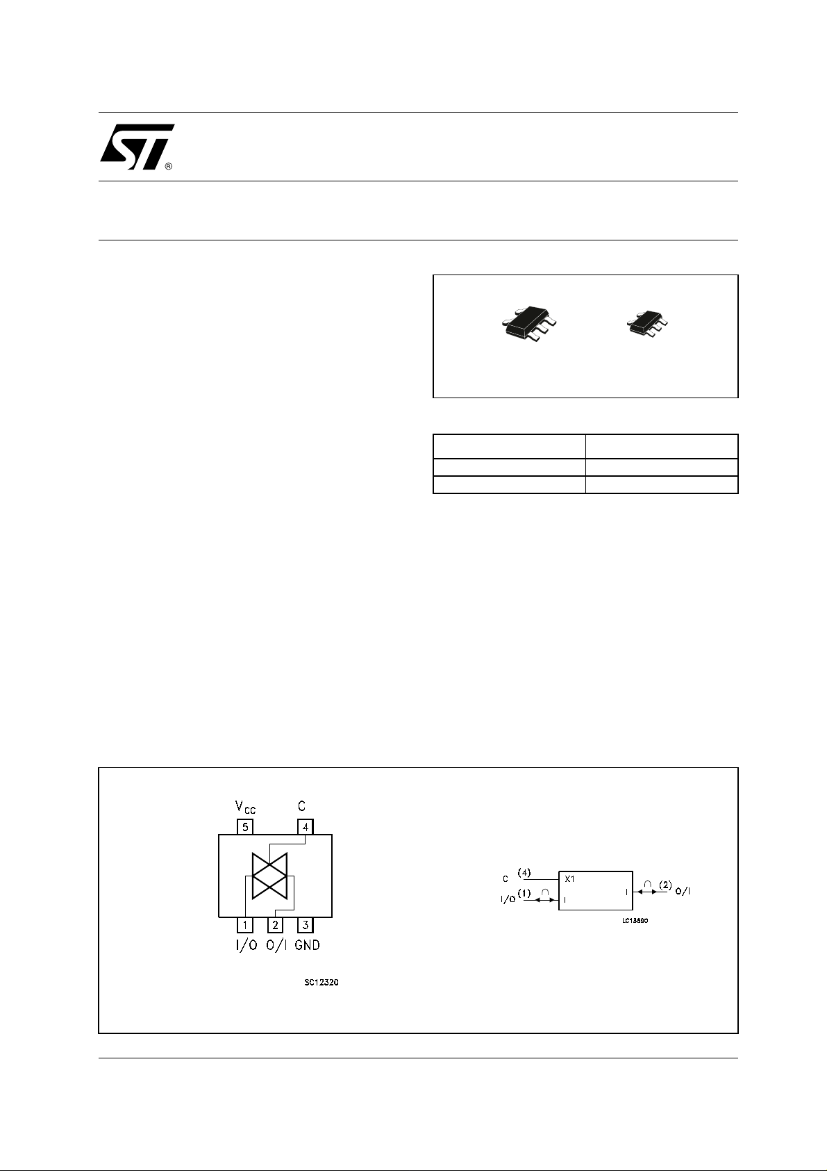
SOT323-5LSOT23-5L
ORDER CODES
PACKAGE T & R
SOT23-5L 74V1G66STR
SOT323-5L 74V1G66CTR
switch is ON (port I/O is connected to Port O/I)
when the C input is held high and OFF (high
impedance state exists between the two ports)
when C is held low. It can be used in many
application as Battery Powered System, Test
Equipment. It’s available in the commercial and
extended temperature range in SOT23-5L and
SC-70-5L package. All inputs and output are
equipped with protection circuits against static
discharge, giving them ESD immunity and
transient excess voltage.
PIN CONNECTION AND IEC LOGIC SYMBOLS
1/11July 2001
Page 2
74V1G66
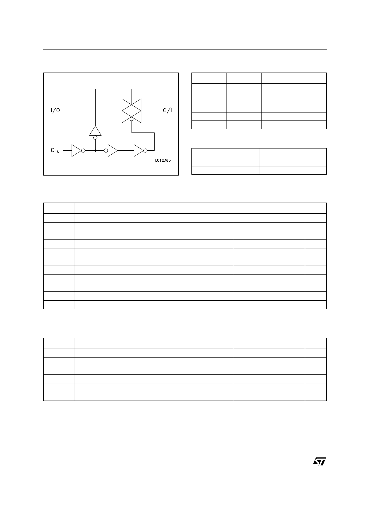
INPUT EQUIVALENT CIRCUIT PIN DESCRIPTION
PIN No SYMBOL NAME AND FUNCTION
1 I/O Independent Input/Output
2 O/I Independent Output/Input
4C
3 GND Ground (0V)
5
V
CC
TRUTH TABLE
CONTROL SWITCH FUNCTION
HON
L OFF *
* : High Impedance S tate
ABSOLUTE MAXIMUM RATINGS
Symbol Parameter Value Unit
V
V
V
V
I
I
I
OK
I
I
or I
CC
T
T
Absolute Maximum Ratings are those values beyond which damage to the device may occur. Functional operation under these conditions is
not implied
Supply Voltage
CC
DC Input Voltage -0.5 to VCC + 0.5
I
DC Control Input Voltage
IC
DC Output Voltage -0.5 to VCC + 0.5
O
DC Input Diode Current
IK
DC Control Input Diode Current
IK
DC Output Diode Current
DC Output Current
O
DC VCC or Ground Current
GND
Storage Temperature
stg
Lead Temperature (10 sec)
L
Enable Input (Active
HIGH)
Positive Supply Voltage
-0.5 to +7.0 V
V
-0.5 to +7.0 V
V
± 20 mA
- 20 mA
± 20 mA
± 50 mA
± 50 mA
-65 to +150 °C
300 °C
RECOMMENDED OPERATING CONDITIONS
Symbol Parameter Value Unit
V
V
V
V
T
dt/dv
1) VIN from 30 % to 70% of VCC on control pi n
2/11
Supply Voltage
CC
Input Voltage 0 to V
I
Control Input Voltage
IC
Output Voltage 0 to V
O
Operating Temperature
op
Input Rise and Fall Time (note 1) V
CC
= 5.0V
2 to 5.5 V
CC
0 to 5.5 V
CC
-55 to 125 °C
0 to 20 ns/V
V
V
Page 3
DC SPECIFICATIONS
Symbol Parameter
V
R
R
I
I
(*) Vol tage range is 3. 3V ± 0.3V
(**) Voltage range is 5V ± 0.5V
High Level Input
IH
Voltage
V
Low Level Input
IL
Voltage
ON Resistance
ON
ON Resistance
ON
Input/Output
OFF
Leakage Current
(SWITCH OFF)
I
Switch Input
IZ
Leakage Current
(SWITCH ON,
OUTPUT OPEN)
I
Control Input
IN
Leakage Current
Quiescent Supply
CC
Current
Test Condition Value
V
(V)
CC
= 25°C
A
Min. Typ. Max. Min. Max. Min. Max.
-40 to 85°C -55 to 125°C
T
2.0 1.5 1.5 1.5
2.7 to
5.5
0.7V
CC
0.7V
CC
0.7V
CC
2.0 0.5 0.5 0.5
2.7 to
5.5
(*)
3.3
(**)
5.0
(*)
3.3
(**)
5.0
VIC = VIH
V
= VCC to GND
I/O
I
≤ 1mA
I/O
VIC = VIH
V
= VCC or GND
I/O
I
≤ 1mA
I/O
0.3V
CC
0.3V
CC
12.5 19 23 27
7.5 10 12 14
8.5 10.5 12.5 15
6.5 8.5 10 12
VOS = VCC to GND
V
5.5
5.5
0 to
5.5
5.5
= VCC to GND
IS
V
= V
IC
= VCC to GND
V
OS
V
= V
IC
V
= 5.5V or GND
IC
= VCC or GND
V
I
IL
IH
±0.1 ± 1 ± 5 µA
±0.1 ± 1 ± 5 µA
± 0.1 ± 1.0 ± 1.0 µA
11020µA
74V1G66
Unit
0.3V
CC
V
V
Ω
Ω
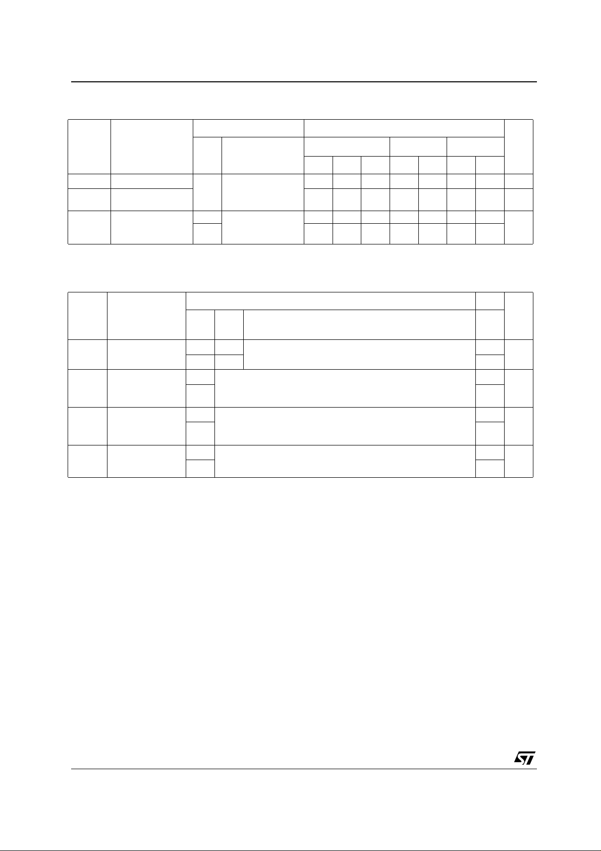
AC ELECTRICAL CHARACTERISTICS (CL = 50pF, Input tr = tf = 3ns)
Test Condition Value
= 25°C
Symbol Parameter
t
t
t
t
t
(*) Vol tage range is 3. 3V ± 0.3V
(**) Voltage range is 5.0V ±
PD
PLZ
PHZ
PZL
PZH
Delay Time
Output Disable
Time
Output Enable
Time
0.5V
V
3.3
5.0
3.3
5.0
3.3
5.0
(V)
CC
(*)
(**)
(*)
(**)
(*)
(**)
tr = tf = 6ns
RL = 500 Ω
RL = 1 KΩ
T
A
Min. Typ. Max. Min. Max. Min. Max.
0.4 0.8 1.2 2.4
0.3 0.6 1.0 2.0
5.0 7.5 9.0 10.0
5.0 7.5 9.0 10.0
2.5 4.0 5.0 7.0
2.0 4.0 5.0 7.0
-40 to 85°C -55 to 125°C
Unit
ns
ns
ns
3/11
Page 4
74V1G66
CAPACITIVE CHARACTERISTICS
Test Condition Value
T
Symbol Parameter
V
CC
(V)
C
C
C
1) CPD is de fined as the value of the IC’s i n t ernal equi v alent capa c itance which is calculated from the op erating current co nsumption without
load. (Refer to Test Circuit). A verage operating current can be obtained by the followi ng equati on. I
Input Capacitance
IN
Output
I/O
Capacitance
Power Dissipation
PD
Capacitance
(note 1)
3.3 2.5
5.0 3
= 25°C
A
Min. Typ. Max. Min. Max. Min. Max.
310 10 10pF
10 pF
ANALOG SWITCH CHARACTERISTICS (GND = 0V; TA = 25°C)
Test Condition Value
Symbol Parameter
Sine Wave
Distortion (THD)
f
MAX
Frequency
Response
(Switch ON)
Feed through
Attenuation
(Switch OFF)
Crosstalk (Control
Input to Signal
Output)
(*)Voltage range is 3.3V ± 0. 3V
(**) Volta ge range is 5.0V ±
0.5V
V
3.3
5.0
3.3
5.0
3.3
5.0
3.3
5.0
(V)
V
IN
CC
(V
)
p-p
(*)
2.75
(**)
4 0.04
(*)
(**)
(*)
(**)
(*)
(**)
Adjust fIN voltage to obtain 0 dBm at VOS.
Increase f
Adjust f
R
= 600Ω, CL = 50 pF, fIN = 1KHz sine wave
L
RL = 600Ω, CL = 50 pF, fIN = 1KHz square wave
= 1 KHz RL = 10 KΩ, CL = 50 pF
f
IN
Frequency until dB meter reads -3dB
IN
R
= 50Ω, CL = 10 pF
L
V
is centered at VCC/2
IN
Voltage to obtained 0dBm at VIS
IN
t
= tf = 6ns
r
-40 to 85°C -55 to 125°C
= CPD x VCC x fIN + I
CC(opr)
CC
Typ.
0.04
150
180
-60
-60
60
60
Unit
pF
Unit
%
MHz
dB
mV
4/11
Page 5

SWITCHING CARACTERISTICS TEST CIRCUIT
74V1G66
FEEDTHROUGH ATTENUATION
BANDWIDTH ATTENUATION
MAXIMUM CONTROL FREQUENCY
CROSSTALK (control to output
5/11
Page 6

74V1G66
CHANNEL RESISTANCE (R
ICC (Opr.)
ON)
6/11
Page 7

74V1G66
SOT23-5L MECHANICAL DATA
mm. mils
DIM.
MIN. TYP MAX. MIN. TYP. MAX.
A 0.90 1.45 35.4 57.1
A1 0.00 0.15 0.0 5.9
A2 0.90 1.30 35.4 51.2
b 0.35 0.50 13.7 19.7
C 0.09 0.20 3.5 7.8
D 2.80 3.00 110.2 118.1
E 2.60 3.00 102.3 118.1
E1 1.50 1.75 59.0 68.8
e0.95 37.4
e1 1.9 74.8
L 0.35 0.55 13.7 21.6
7/11
Page 8

74V1G66
SOT323-5L MECHANICAL DATA
mm. mils
DIM.
MIN. TYP MAX. MIN. TYP. MAX.
A 0.80 1.10 31.5 43.3
A1 0.00 0.10 0.0 3.9
A2 0.80 1.00 31.5 39.4
b 0.15 0.30 5.9 11.8
C 0.10 0.18 3.9 7.1
D 1.80 2.20 70.9 86.6
E 1.80 2.40 70.9 94.5
E1 1.15 1.35 45.3 53.1
e0.65 25.6
e1 1.3 51.2
L 0.10 0.30 3.9 11.8
8/11
Page 9

Tape & Reel SOT23-xL MECHANICAL DATA
74V1G66
DIM.
MIN. TYP MAX. MIN. TYP. MAX.
A 180 7.086
C 12.8 13.0 13.2 0.504 0.512 0.519
D 20.2 0.795
N 60 2.362
T 14.4 0.567
Ao 3.13 3.23 3.33 0.123 0.127 0.131
Bo 3.07 3.17 3.27 0.120 0.124 0.128
Ko 1.27 1.37 1.47 0.050 0.054 0.0.58
Po 3.9 4.0 4.1 0.153 0.157 0.161
P 3.9 4.0 4.1 0.153 0.157 0.161
mm. inch
9/11
Page 10

74V1G66
Tape & Reel SOT323-xL MECHANICAL DATA
DIM.
MIN. TYP MAX. MIN. TYP. MAX.
A 175 180 185 6.889 7.086 7.283
C 12.8 13 13.2 0.504 0.512 0.519
D 20.2 0.795
N 59.5 60 60.5 2.362
T 14.4 0.567
Ao 2.25 0.088
Bo 2.7 0.106
Ko 1.2 0.047
Po 3.98 4 4.2 0.156 0.157 0.165
P 3.98 4 4.2 0.156 0.157 0.165
mm. inch
10/11
Page 11

74V1G66
Information furnished is bel ieved to be accurate and reliable. However, STMicroe lectronics assumes no responsibility for the
consequences of use of such information nor for any infringement of patents or other rights of third parties which may result from
its use. No li cense is granted by i mp lication or otherwise under any patent or patent rights of STMicroelec tron ic s. S pec ificat ions
mentioned in this publication ar e subject to change without notice. This publication supersedes and replaces all information
previously supplied. S TMicroelectronics products are not authorized for use as critica l components in life suppo rt devices or
systems without express written approval of STMicroelectronics.
Australi a - Brazil - Chi n a - Finland - F rance - Germ any - Hong Kong - India - It al y - Japan - Ma l aysia - Malta - Morocco
© The ST logo is a registered trademark of STMicroelectronics
© 2001 STM icroelectronics - P r i n ted in Italy - All Rights Reserved
STMicr o el ectronics GROUP OF COMPA NI ES
Singapo re - Spain - Sweden - Switzerland - United Ki ngdom
© http://www.st.com
11/11
 Loading...