

Page 1
1/9May 2002
■ HIGH SPEED: t
PD
= 0.5ns (TYP.) at VCC = 5V
■ LOW POWER DISSIPATION:
I
CC
= 1µA(MAX.) at TA=25°C
■ LOW "ON" RESISTANCE at V
CC
=5.0V:
R
ON
= 7Ω (TYP) , VIN=0V, I
I/O
=30mA
R
ON
= 20Ω (TYP), VIN=2.4V , I
I/O
=10mA
■ OPERATING VOLATGE RANGE:
V
CC
(OPR.) = 3.0V TO 5.5V
■ 5V TOLERANT ON CONTROL PIN
■ HIGH NOISE IMMUNITY:
V
NIH
= V
NIL
= 28% VCC (MIN.)
DESCRIPTION
The 74V1G384 is an advanced high-speed CMOS
SINGLE HIGH SPEED BUS SWITCH fabricated
in silicon gate C
2
MOS technology. It’s designed
to operate from 3V to 5.5V, making this device
ideal for portable applications. It’s offers 7Ω
Resistance typical value at V
CC
=4.5V. Additional
key feature are fast switching speed (t
ON
=3.8ns,
t
OFF
=3.3ns Typical) and Low Power
Consumption.
The OE
input is provided to control the switch; the
switch is ON when the OE
input is h eld low and
OFF when OE
is held high.
It’s available in the commercial and extended
temperature range in SOT23-5L and SC-70-5L
package.
74V1G384
SINGLE HIGH SPEED BUS SWITCH
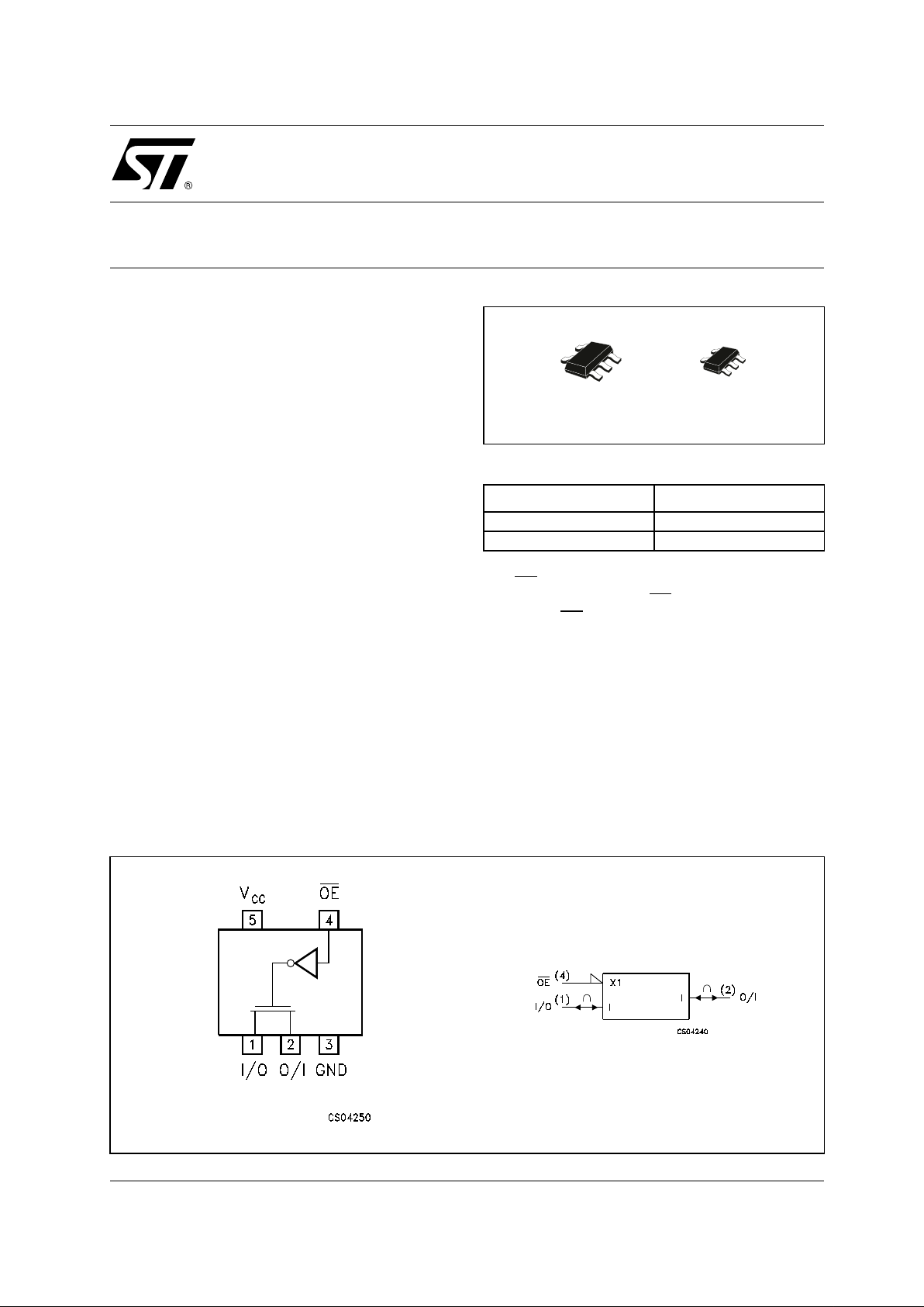
PIN CONNECTION AND IEC LOGIC SYMBOLS
ORDER CODES
PACKAGE T & R
SOT23-5L 74V1G384STR
SOT323-5L 74V1G384CTR
SOT323-5LSOT23-5L
Page 2
74V1G384
2/9
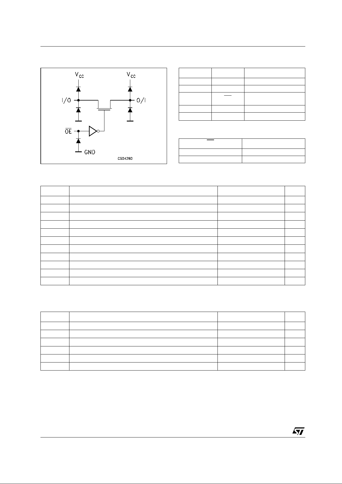
INPUT EQUIVALENT CIRCUIT PIN DESCRIPTION
TRUTH TABLE
* High Impedance State
ABSOLUTE MAXIMUM RATINGS
Absolute Maximum Ratings are those values beyond which damage to the device may occur. Functional operation under these conditions is
not implied.
RECOMMENDED OPERATING CONDITIONS
1) VIN from 30 % to 70% of V
CC
on control pi n
PIN No SYMBOL NAME AND FUNCTION
1 I/O Independent Input/Output
2 O/I Independent Output/Input
4OE
Enable Input (Active
HIGH)
3 GND Ground (0V)
5
V
CC
Positive Supply Voltage
OE
SWITCH FUNCTION
LON
H OFF *
Symbol Parameter Value Unit
V
CC
Supply Voltage
-0.5 to +7.0 V
V
I
DC Input Voltage -0.5 to VCC + 0.5
V
V
IC
DC Control Input Voltage
-0.5 to +7.0 V
V
O
DC Output Voltage -0.5 to VCC + 0.5
V
I
IK
DC Input Diode Current
±
20 mA
I
IK
DC Control Input Diode Current
- 20 mA
I
OK
DC Output Diode Current
±
20 mA
I
O
DC Output Current
±
50 mA
I
CC
or I
GND
DC VCC or Ground Current
±
50 mA
T
stg
Storage Temperature
-65 to +150 °C
T
L
Lead Temperature (10 sec)
300 °C
Symbol Parameter Value Unit
V
CC
Supply Voltage
3 to 5.5 V
V
I
Input Voltage 0 to V
CC
V
V
IC
Control Input Voltage
0 to 5.5 V
V
O
Output Voltage 0 to V
CC
V
T
op
Operating Temperature
-55 to 125 °C
dt/dv
Input Rise and Fall Time (note 1) V
CC
= 5.0V
0 to 20 ns/V
Page 3
74V1G384
3/9
DC SPECIFICATIONS
AC ELECTRICAL CHARACTERISTICS (C
L
= 50pF, Input tr = tf = 3ns)
(*) Vol tage range is 3.3V ± 0.3V
(**) Voltage range is 5.0V
±
0.5V
Symbol Parameter
Test Condition Value
Unit
V
CC
(V)
T
A
= 25°C
-40 to 85°C -55 to 125°C
Min. Typ. Max. Min. Max. Min. Max.
V
IH
High Level Input
Voltage
2.0 1.5 1.5 1.5
V
3.0 to
5.5
0.7V
CC
0.7V
CC
0.7V
CC
V
IL
Low Level Input
Voltage
2.0 0.5 0.5 0.5
V
3.0 to
5.5
0.3V
CC
0.3V
CC
0.3V
CC
R
ON
ON Resistance 3.0 VIC = VIL
V
I/O
= GND
I
I/O
≤ 30 mA
91320
Ω
4.5 V
IC
= VIL
V
I/O
= GND
I
I/O
≤ 30 mA
71015
Ω
R
ON
ON Resistance 3.0 VIC = VIL
V
I/O
= 1.5V
I
I/O
≤ 10 mA
32 60 80
Ω
4.5 V
IC
= VIL
V
I/O
= 2.4V
I
I/O
≤ 10 mA
20 40 60
Ω
I
OFF
Input/Output
Leakage Current
(SWITCH OFF)
5.5
VOS = VCC to GND
V
IS
= VCC to GND
V
IC
= V
IL
±
0.1
±
1
±
10µA
I
IN
Control Input
Leakage Current
0 to
5.5
V
IC
= 5.5V or GND
±
0.1
±
1.0
±
1.0µA
I
CC
Quiescent Supply
Current
5.5
V
I
= VCC or GND
11020
µ
A
Symbol Parameter
Test Condition Value
Unit
V
CC
(V)
T
A
= 25°C
-40 to 85°C -55 to 125°C
Min. Typ. Max. Min. Max. Min. Max.
t
PD
Delay Time
3.3
(*)
tr = tf = 6ns
0.8 1.2 1.5 2.0
ns
5.0
(**)
tr = tf = 6ns
0.5 0.8 1.0 1.5
t
PLZ
t
PHZ
Output Disable
Time
3.3
(*)
R1 = 500Ω
VIN=1.5V
8.5 12.0 14.0 16.0 ns
5.0
(**)
R1 = 500 Ω
VIN=2.4V
3.8 6.5 9.0 10.0
t
PZL
t
PZH
Output Enable
Time
3.3
(*)
R1 = 1KΩ
VIN=1.5V
7.3 12.0 14.0 16.0
ns
5.0
(**)
R1 = 1KΩ
VIN=2.4V
3.3 5.0 7.5 8.5
Page 4

74V1G384
4/9
CAPACITIVE CHARACTERISTICS
1) CPD is de fined as t he value of the IC’ s i nternal equivale nt capaci tance whic h is calculated fr o m t he operat i ng current consumpt i on without
load. (Refer to Test Cir cuit). Average operatin g current can be obtained by the followin g equation. I
CC(opr)
= CPD x VCC x fIN + I
CC
Symbol Parameter
Test Condition Value
Unit
V
CC
(V)
T
A
= 25°C
-40 to 85°C -55 to 125°C
Min. Typ. Max. Min. Max. Min. Max.
C
IN
Input Capacitance
410 10 10pF
C
I/O
Output
Capacitance
7pF
C
PD
Power Dissipation
Capacitance
(note 1)
3.3 2.5
pF
5.0 3
Page 5

74V1G384
5/9
DIM.
mm. mils
MIN. TYP MAX. MIN. TYP. MAX.
A 0.90 1.45 35.4 57.1
A1 0.00 0.15 0.0 5.9
A2 0.90 1.30 35.4 51.2
b 0.35 0.50 13.7 19.7
C 0.09 0.20 3.5 7.8
D 2.80 3.00 110.2 118.1
E 2.60 3.00 102.3 118.1
E1 1.50 1.75 59.0 68.8
e0.95 37.4
e1 1.9 74.8
L 0.35 0.55 13.7 21.6
SOT23-5L MECHANICAL DATA
Page 6

74V1G384
6/9
DIM.
mm. mils
MIN. TYP MAX. MIN. TYP. MAX.
A 0.80 1.10 31.5 43.3
A1 0.00 0.10 0.0 3.9
A2 0.80 1.00 31.5 39.4
b 0.15 0.30 5.9 11.8
C 0.10 0.18 3.9 7.1
D 1.80 2.20 70.9 86.6
E 1.80 2.40 70.9 94.5
E1 1.15 1.35 45.3 53.1
e0.65 25.6
e1 1.3 51.2
L 0.10 0.30 3.9 11.8
SOT323-5L MECHANICAL DATA
Page 7

74V1G384
7/9
DIM.
mm. inch
MIN. TYP MAX. MIN. TYP. MAX.
A 180 7.086
C 12.8 13.0 13.2 0.504 0.512 0.519
D 20.2 0.795
N 60 2.362
T 14.4 0.567
Ao 3.13 3.23 3.33 0.123 0.127 0.131
Bo 3.07 3.17 3.27 0.120 0.124 0.128
Ko 1.27 1.37 1.47 0.050 0.054 0.0.58
Po 3.9 4.0 4.1 0.153 0.157 0.161
P 3.9 4.0 4.1 0.153 0.157 0.161
Tape & Reel SOT23-xL MECHANICAL DATA
Page 8

74V1G384
8/9
DIM.
mm. inch
MIN. TYP MAX. MIN. TYP. MAX.
A 175 180 185 6.889 7.086 7.283
C 12.8 13 13.2 0.504 0.512 0.519
D 20.2 0.795
N 59.5 60 60.5 2.362
T 14.4 0.567
Ao 2.25 0.088
Bo 2.7 0.106
Ko 1.2 0.047
Po 3.98 4 4.2 0.156 0.157 0.165
P 3.98 4 4.2 0.156 0.157 0.165
Tape & Reel SOT323-xL MECHANICAL DATA
Page 9

74V1G384
9/9
Information furnished is believed to be accurate and reliable. However, STMicroelectronics assumes no responsibility f or the
consequences of use of such informatio n nor for any infringement of paten ts or o ther rig hts of t hird part ies which ma y result from
its use. No license is granted by implication or otherwise under any patent or patent rights of STMicroelectronics. Specifications
mentioned in this publication are subject to change without notice. This publication supersedes and replaces all information
previousl y suppl ied. STM icroel ectronics produc ts are not auth orized for use as c ritica l compone nts in l ife s upport dev ices or
systems without express written approval of STMicroelectronics.
© The ST logo is a registered trademark of STMicroelectronics
© 2002 STMicroelectronics - Prin ted in Italy - All Rights Reserved
STMicroelectronics GROUP OF COMPANIES
Australia - Brazil - Canada - China - Finland - France - Germany - Hong Kong - India - Israel - Italy - Japan - Malaysia - Malta - Morocco
Singapore - Spain - Sweden - Switzerland - United Kingdom - United States.
© http://www.st.com
 Loading...