

Page 1
查询74V1G384供应商
74V1G384
SINGLE HIGH SPEED BUS SWITCH
■ HIGH SPEED: t
■ LOW POWER DISSIPATION:
I
=1µA(MAX.) at TA=25°C
CC
■ LOW "ON" RESISTANCE at V
R
=7Ω (TYP), VIN=0V, I
ON
R
=14Ω (TYP), VIN=2.4V, I
ON
■ OPERATING VOLATGE RANGE:
V
(OPR.) = 3.0V TO 5.5V
CC
■ 5V TOLERANT ON CONTROL PIN
■ HIGH NOISE IMMUNITY:
V
NIH=VNIL
= 28% VCC(MIN.)
= 0.5ns (TYP.) at VCC=5V
PD
=5.0V:
CC
=30mA
I/O
=15mA
I/O
DESCRIPTION
The 74V1G384 is anadvanced high-speed CMOS
SINGLE HIGH SPEED BUS SWITCH fabricated
in silicongate C
2
MOS technology. It’s designed to
operate from 3V to 5. 5V , making this device ideal
for portable applications. It’s offers 7Ω Resistance
typical value at V
are fast switching speed (t
=5V. Additional key feature
CC
=3.8ns, t
ON
OFF
=3.3ns
Typical) and Low Power Consumption.
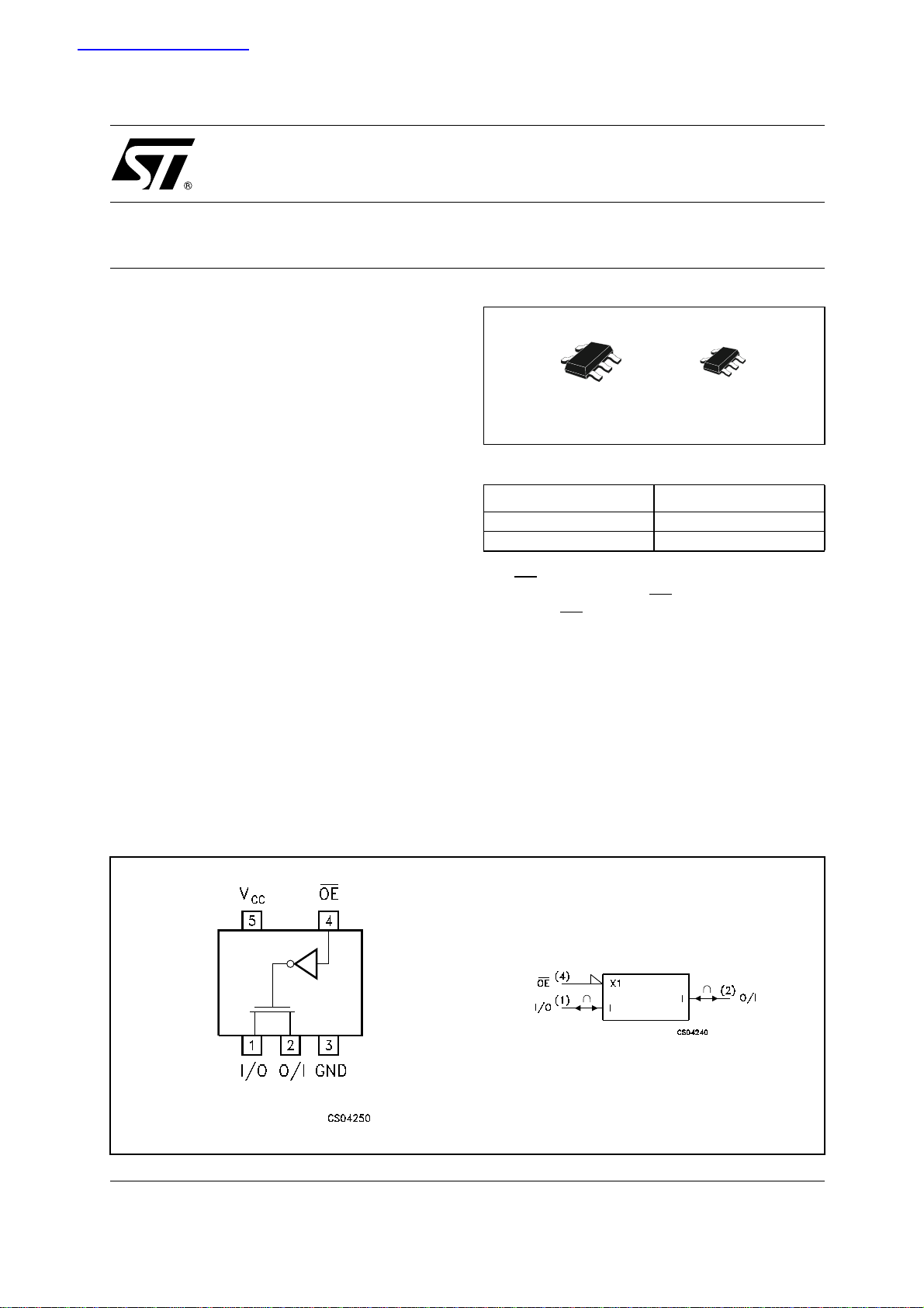
SOT323-5LSOT23-5L
ORDER CODES
PACKAGE T & R
SOT23-5L 74V1G384STR
SOT323-5L 74V1G384CTR
TheOE
switch is ON when the OE
OFF when OE
input is provided to control the sw itch; the
input is held low and
is held high.
It’s available in the commercial and extended
temperature range in SOT23-5L and SC-70-5L
package.
PIN CONNECTION AND IEC LOGIC SYMBOLS
1/9April 2004
Page 2
74V1G384
INPUT EQUIVALENT CIRCUIT PIN DESCRIPTION
PIN N° SYMBOL NAME AND FUNCTION
1 I/O Independent Input/Output
2 O/I Independent Output/Input
4OE
3 GND Ground (0V)
5
TRUTH TABLE
V
CC
Enable Input (Active
HIGH)
Positive Supply Voltage
OE
SWITCH FUNCTION
LON
HOFF*
* High Impedance State
ABSOLUTE MAXIMUM RATINGS
Symbol Parameter Value Unit
V
V
V
V
I
I
I
OK
I
or I
I
CC
T
T
Absolute Maximum Ratings are those values beyond which damage to the device may occur. Functional operation under these conditions is
not implied.
Supply Voltage
CC
DC Input Voltage -0.5 to VCC+0.5
I
DC Control Input Voltage
IC
DC Output Voltage -0.5 to VCC+0.5
O
DC Input Diode Current
IK
DC Control Input Diode Current
IK
DC Output Diode Current
DC Output Current
O
DC VCCor Ground Current
GND
Storage Temperature
stg
Lead Temperature (10 sec)
L
-0.5 to +7.0 V
V
-0.5 to +7.0 V
V
± 20 mA
-20 mA
± 20 mA
± 50 mA
± 50 mA
-65 to +150 °C
300 °C
RECOMMENDED OPERATING CONDITIONS
Symbol Parameter Value Unit
V
V
V
V
T
dt/dv
1) VINfrom30%to70%ofVCCon control pin
Supply Voltage
CC
Input Voltage 0 to V
I
Control Input Voltage
IC
Output Voltage 0 to V
O
Operating Temperature
op
Input Rise and Fall Time (note 1) V
CC
=5.0V
3to5.5 V
CC
0to5.5 V
CC
-55 to 125 °C
0 to 20 ns/V
2/9
V
V
Page 3
DC SPECIFICATIONS
Symbol Parameter
V
R
R
I
High Level Input
IH
Voltage
V
Low Level Input
IL
Voltage
ON Resistance
ON
ON Resistance 3.0 VIC=V
ON
Input/Output
OFF
Leakage Current
(SWITCH OFF)
Control Input
I
IN
Leakage Current
I
Quiescent Supply
CC
Current
Test Condition Value
V
(V)
CC
= 25°C
A
Min. Typ. Max. Min. Max. Min. Max.
-40 to 85°C -55 to 125°C
T
2.0 1.5 1.5 1.5
3.0to
5.5
0.7V
CC
0.7V
CC
0.7V
CC
2.0 0.5 0.5 0.5
3.0to
5.5
3.0
4.5
4.5 V
VIC=V
V
I/O
I
≤ 30 mA
I/O
V
IC=VIL
V
I/O
I
≤ 30 mA
I/O
V
I/O
I
≤ 15 mA
I/O
IC=VIL
V
I/O
I
≤ 15 mA
I/O
IL
=GND
=GND
IL
=1.5V
=2.4V
0.3V
CC
0.3V
CC
91320Ω
71015Ω
20 40 60 Ω
14 28 40 Ω
VOS=VCCto GND
5.5
0to
5.5
5.5
V
IS=VCC
V
IC
V
I=VCC
to GND
V
IC=VIL
=5.5VorGND
or GND
±0.1 ± 1 ± 10 µA
± 0.1 ± 1.0 ± 1.0 µA
11020µA
74V1G384
Unit
V
CC
V
0.3V
AC ELECTRICAL CHARACTERISTICS (C
Test Condition Value
Symbol Parameter
t
t
PLZ
t
PHZ
t
PZL
t
PZH
(*) Voltage rangeis3.3V± 0.3V
(**) Voltage range is 5.0V ± 0.5V
PD
Delay Time
Output Disable
Time
Output Enable
Time
V
3.3
5.0
3.3
5.0
3.3
5.0
(V)
CC
(*)
(**)
(*)
(**)
(*)
(**)
tr=tf=6ns
tr=tf=6ns
R1= 500Ω
VIN=1.5V
R1= 500Ω
VIN=2.4V
R1=1KΩ
VIN=1.5V
R1=1KΩ
VIN=2.4V
= 50pF, Input tr=tf= 3ns)
L
= 25°C
T
A
Min. Typ. Max. Min. Max. Min. Max.
0.8 1.2 1.5 2.0
0.5 0.8 1.0 1.5
8.5 12.0 14.0 16.0 ns
3.8 6.5 9.0 10.0
7.3 12.0 14.0 16.0
3.3 5.0 7.5 8.5
-40 to 85°C -55 to 125°C
Unit
ns
ns
3/9
Page 4

74V1G384
CAPACITIVE CHARACTERISTICS
Test Condition Value
T
Symbol Parameter
V
CC
(V)
C
C
C
1) CPDis defined as the value of the IC’s internal equivalent capacitance which is calculated from the operating current consumption without
load. (Refer to Test Circuit). Average operating current can be obtained by the following equation. I
Input Capacitance
IN
Output
I/O
Capacitance
Power Dissipation
PD
Capacitance
(note 1)
3.3 2.5
5.0 3
=25°C
A
Min. Typ. Max. Min. Max. Min. Max.
410 10 10pF
7pF
-40 to 85°C -55 to 125°C
CC(opr)=CPDxVCCxfIN+ICC
Unit
pF
4/9
Page 5

74V1G384
SOT23-5L MECHANICAL DATA
mm. mils
DIM.
MIN. TYP MAX. MIN. TYP. MAX.
A 0.90 1.45 35.4 57.1
A1 0.00 0.10 0.0 3.9
A2 0.90 1.30 35.4 51.2
b 0.35 0.50 13.7 19.7
C 0.09 0.20 3.5 7.8
D 2.80 3.00 110.2 118.1
E 1.50 1.75 59.0 68.8
e0.95 37.4
H 2.60 3.00 102.3 118.1
L 0.10 0.60 3.9 23.6
.
7049676C
5/9
Page 6

74V1G384
SOT323-5L MECHANICAL DATA
mm. mils
DIM.
MIN. TYP MAX. MIN. TYP. MAX.
A 0.80 1.10 31.5 43.3
A1 0.00 0.10 0.0 3.9
A2 0.80 1.00 31.5 39.4
b 0.15 0.30 5.9 11.8
C 0.10 0.18 3.9 7.1
D 1.80 2.20 70.9 86.6
E 1.80 2.40 70.9 94.5
E1 1.15 1.35 45.3 53.1
e
e1 1.3 51.2
L 0.10 0.30 3.9 11.8
.65
0
25.6
6/9
Page 7

Tape & Reel SOT23-xL MECHANICAL D ATA
74V1G384
DIM.
MIN. TYP MAX. MIN. TYP. MAX.
A 180 7.086
C 12.8 13.0 13.2 0.504 0.512 0.519
D 20.2 0.795
N 60 2.362
T 14.4 0.567
Ao 3.13 3.23 3.33 0.123 0.127 0.131
Bo 3.07 3.17 3.27 0.120 0.124 0.128
Ko 1.27 1.37 1.47 0.050 0.054 0.0.58
Po 3.9 4.0 4.1 0.153 0.157 0.161
P 3.9 4.0 4.1 0.153 0.157 0.161
mm. inch
7/9
Page 8

74V1G384
Tape & Reel SOT323-xL MECHANICAL DATA
DIM.
MIN. TYP MAX. MIN. TYP. MAX.
A 175 180 185 6.889 7.086 7.283
C 12.8 13 13.2 0.504 0.512 0.519
D 20.2 0.795
N 59.5 60 60.5 2.362
T 14.4 0.567
Ao 2.25 0.088
Bo 2.7 0.106
Ko 1.2 0.047
Po 3.9 4 4.1 0.153 0.157 0.161
P 3.8 4 4.2 0.149 0.157 0.165
mm. inch
8/9
Page 9

74V1G384
Information furnished is believed to be accurate and reliable. However, STMicroelectronics assumes no responsibility for the
consequences of use of such inform ation nor fo r an y infring ement of p atents or o ther rights of third p arties which may r esult f rom
its use. No license is granted by implication or otherwise under any patent or patent rights of STMicroelectronics. Specifications
mentioned in this publication are subject to change without notice. This publication supersedes and replaces all information
previously supplied. STMicroelectronics products ar e not authorized for use as critical components in life support devices or
systems without express written approval of STMicroelectronics.
Australia - Belgium - Brazil - Canada - China - Czech Republic - Finland - France - Germany - Hong Kong - India - Israel - Italy - Japan -
Malaysia - Malta - Morocco - Singapore - Spain - Sweden - Switzerland - United Kingdom - United States.
The ST logo is a registered trademark of STMicroelectronics
All other names are the property of their respective owners
© 2004 STMicroelectronics - All Rights Reserved
STMicroelectronics GROUP OF COMPANIES
http://www.st.com
9/9
 Loading...