

Page 1
■ HIGHSPEED:t
■
LOW POWER DISSIPATION:
I
=1 µA (MAX.)at TA=25oC
CC
■
HIGHNOISEIMMUNITY:
V
NIH=VNIL
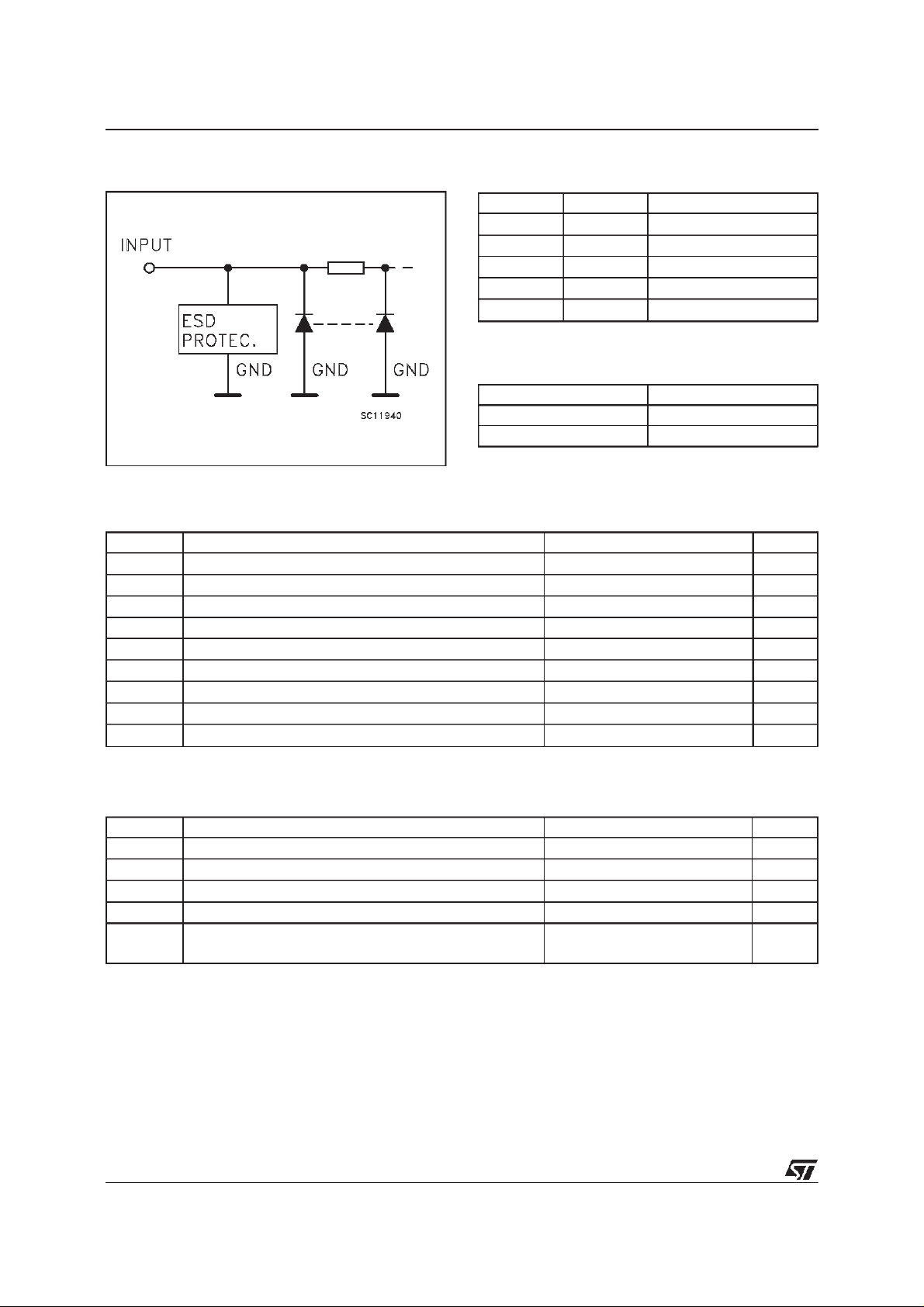
■ POWERDOWNPROTECTIONON INPUT
■
OPERATINGVOLTAGERANGE:
V
CC
■ IMPROVEDLATCH-UPIMMUNITY
=28%VCC(MIN.)
(OPR)= 2Vto5.5V
=6.1ns(TYP.)atVCC=5V
PD
74V1G07
SINGLE BUFFER (OPEN DRAIN)
PRELIMINARY DATA
S
(SOT23-5L)
ORDERCODE:
74V1G07S 74V1G07C
C
(SC-70)
DESCRIPTION
The 74V1G07 is an advancedhigh-speed CMOS
SINGLE BUFFER (OPEN DRAIN) fabricated with
sub-micron silicon gate and double-layer metal
wiringC
2
MOStechnology.
The internal circuit is composed of 2 stages
including buffer output, which provide high noise
immunityand stableoutput.
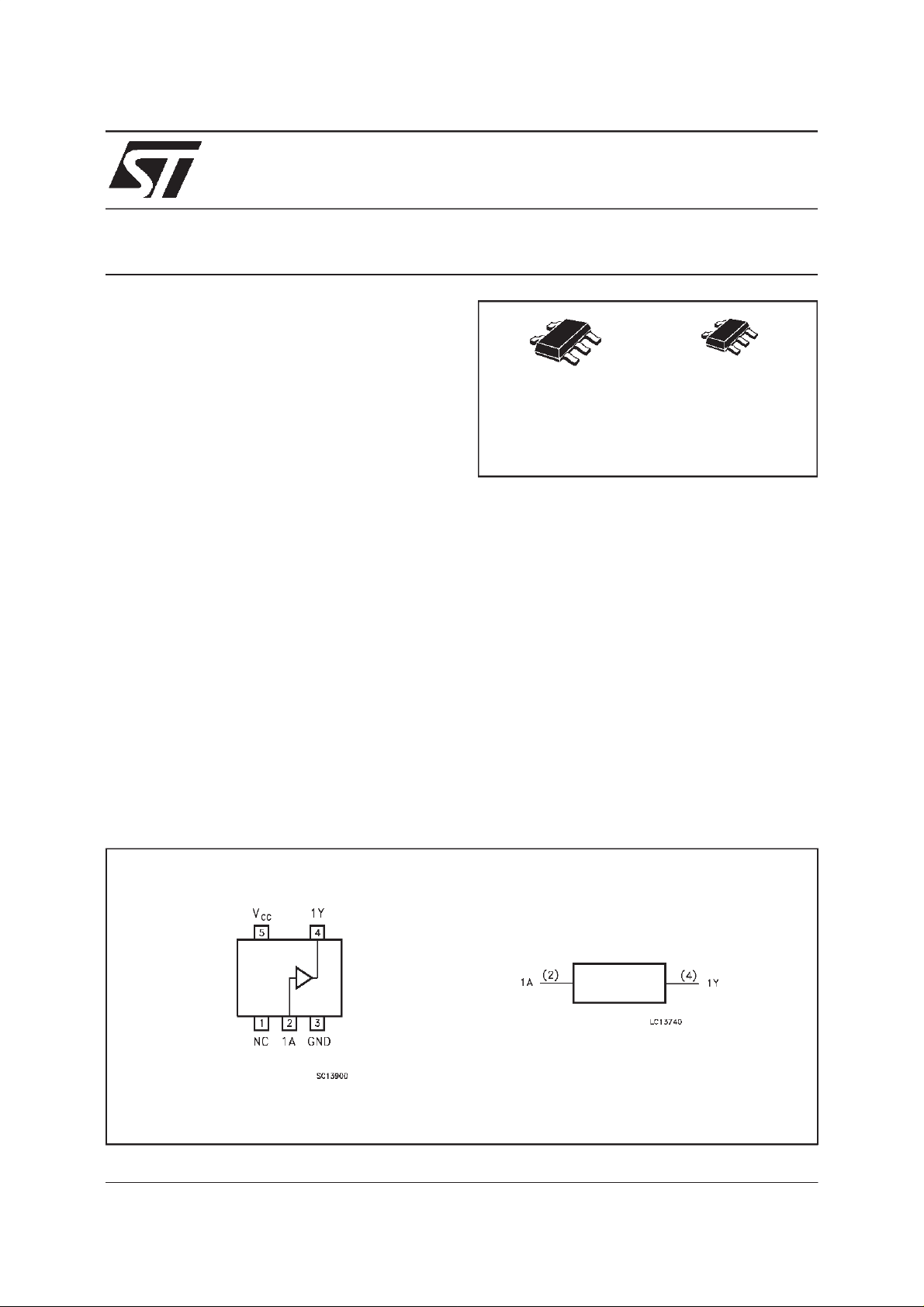
PIN CONNECTION AND IEC LOGIC SYMBOLS
Power down protection is provided on input and 0
to 7V can be accepted on inputwith no regard to
the supply voltage. This device can be used to
interface5V to 3V.
October 1999
1/7
Page 2
74V1G07
INPUT EQUIVALENTCIRCUIT
PIN DESCRIPTION
PI N No SYMB OL NAME AND FU NCTIO N
1 N.C. Not Connected
2 1A Data Input
4 1Y Data Output
3 GND Ground (0V)
5V
CC
Positive Supply Voltage
TRUTH TABLE
AY
LL
HZ
Z = High impedance
ABSOLUTE MAXIMUM RATINGS
Symb o l Para met er Val u e Uni t
V
V
V
I
I
OK
I
or I
I
CC
T
T
AbsoluteMaximumRatingsarethosevaluesbeyondwhichdamageto thedevicemayoccur.Functionaloperation underthesecondition isnotimplied.
Supply Voltage -0.5 to +7.0 V
CC
DC Input Voltage -0.5 to +7.0 V
I
DC Output Voltage -0.5 to VCC+ 0.5 V
O
DC Input Diode Current - 20 mA
IK
DC Output Diode Current ± 20 mA
DC Output Current
O
DC VCCor Ground Current
GND
Storage Temperature -65 to +150
stg
Lead Temperature (10 sec) 260
L
25 mA
±
50 mA
±
o
C
o
C
RECOMMENDED OPERATINGCONDITIONS
Symb o l Para met er Value Un it
V
V
V
T
dt/dv
1)VINfrom30%to70%of V
2/7
Supply Voltage 2.0 to 5.5 V
CC
Input Voltage 0 to 5.5 V
I
Output Voltage 0 to V
O
Operating Temperature -40 to +85
op
(V
CC
CC
=3.3±0.3V)
=5.0±0.5V)
Input Rise and Fall Time (see note 1) (V
CC
CC
0 to 100
0to20
V
o
C
ns/V
ns/V
Page 3
74V1G07
DC SPECIFICATIONS
Symb o l Para met er Test C o n dit io ns Val u e Uni t
T
V
CC
(V)
High Level Input
V
IH
Voltage
V
Low Level Input
IL
Voltage
V
Low Level Output
OL
Voltage
2.0 1.5 1.5
3.0 to 5.5 0.7V
2.0 0.5 0.5
3.0 to 5.5 0.3V
2.0 IO=50 µ A 0.0 0.1 0.1
3.0 I
4.5 I
3.0 I
4.5 I
High Impedance
I
OZ
Output Leakage
5.5
VO=VCCor GND
Current
Input Leakage Current 0 to 5.5 VI= 5.5V or GND
I
I
Quiescent Supply
I
CC
5.5 VI=VCCorGND 1 10
Current
Min. Typ. Max. Min. Max.
=50µA 0.0 0.1 0.1
O
=50µA 0.0 0.1 0.1
O
=4 mA 0.36 0.44
O
=8 mA 0.36 0.44
O
VI=VIHor V
IL
=25oC -40 to 85oC
A
CC
0.7V
CC
±0.25 ±2.5 µA
0.1
±
CC
0.3V
±
1.0
CC
µ
µ
V
V
V
A
A
AC ELECTRICAL CHARACTERISTICS (Input tr=tf=3 ns)
Symbol Parameter Test Condition Value Unit
t
Propagation Delay
PLH
Time
t
PHL
(*) Voltagerangeis 3.3V± 0.3V
(**) Voltagerangeis 5V± 0.5V
V
3.3
3.3
5.0
5.0
CC
(V)
(**)
(**)
C
L
(pF)
(*)
15 7.0 9.7 1.0 11.5
(*)
50 9.5 13.2 1.0 15.0
Min. Typ. Max. Min. Max.
=25oC -40 to 85oC
T
A
15 4.6 6.8 1.0 8.0
50 6.1 8.8 1.0 10.0
ns
CAPACITIVE CHARACTERISTICS
Symb o l Para met er Test C o n dit io ns Val u e Uni t
=25oC -40 to 85oC
T
A
Min. Typ. Max. Min. Max.
Input Capacitance 4 10 10
C
IN
Power Dissipation
C
PD
11 pF
Capacitance (note 1)
1)CPDisdefined asthevalue oftheIC’sinternal equivalentcapacitance whichis calculated fromtheoperatingcurrent consumptionwithout load.(Referto
TestCircuit).Average operatingcurrent canbeobtainedbythefollowingequation.I
(opr)= CPD• VCC• fIN+I
CC
CC
pF
3/7
Page 4

74V1G07
TESTCIRCUIT
CL= 15/50 pF orequ ivalent (includes jigand probe capacitance)
R
=1KΩ orequivalent
L=R1
R
WAVEFORM:PROPAGATIONDELAYS (f=1MHz; 50% duty cycle)
ofpulse generator (typically50Ω)
T=ZOUT
4/7
Page 5

SOT23-5L MECHANICAL DATA
74V1G07
DIM.
MIN. TYP. MAX. MIN. TYP. MAX.
A 0.90 1.45 35.4 57.1
A1 0.00 0.15 0.0 5.9
A2 0.90 1.30 35.4 51.2
b 0.35 0.50 13.7 19.7
C 0.09 0.20 3.5 7.8
D 2.80 3.00 110.2 118.1
E 2.60 3.00 102.3 118.1
E1 1.50 1.75 59.0 68.8
L 0.35 0.55 13.7 21.6
e 0.95 37.4
e1 1.9 74.8
mm mils
5/7
Page 6

74V1G07
SC-70 MECHANICAL DATA
DIM.
MIN. TYP. MAX. MIN. TYP. MAX.
A 0.80 1.10 31.5 43.3
A1 0.00 0.10 0.0 3.9
A2 0.80 1.00 31.5 39.4
b 0.15 0.30 5.9 11.8
C 0.10 0.18 3.9 7.1
D 1.80 2.20 70.9 86.6
E 1.80 2.40 70.9 94.5
E1 1.15 1.35 45.3 53.1
L 0.10 0.30 3.9 11.8
e 0.65 25.6
e1 1.3 51.2
mm mils
6/7
Page 7

74V1G07
Information furnished isbelieved to be accurate andreliable. However, STMicroelectronics assumes no responsibility for the consequences
of use of such information nor for any infringement of patents or other rights of third parties which may result from its use. No license is
granted by implication or otherwise under any patent or patent rights of STMicroelectronics. Specification mentioned in this publication are
subject tochange without notice. Thispublication supersedes andreplaces all information previously supplied. STMicroelectronics products
are not authorized for use as critical components in life support devices or systems withoutexpress written approval of STMicroelectronics.
The ST logo is a registeredtrademark of STMicroelectronics
1999 STMicroelectronics – Printed in Italy– All RightsReserved
STMicroelectronics GROUP OF COMPANIES
Australia - Brazil - China - Finland -France - Germany - Hong Kong - India - Italy- Japan - Malaysia - Malta - Morocco
Singapore - Spain- Sweden - Switzerland - United Kingdom - U.S.A.
http://www.st.com
.
7/7
 Loading...