

Page 1
74V1G05
SINGLE INVERTER (OPEN DRAIN)
■ HIGH SPEED: t
■ LOW POWER DISSIPATION:
I
=1µA(MAX.) at TA=25°C
CC
■ HIGH NOISE IMMUNITY:
V
NIH=VNIL
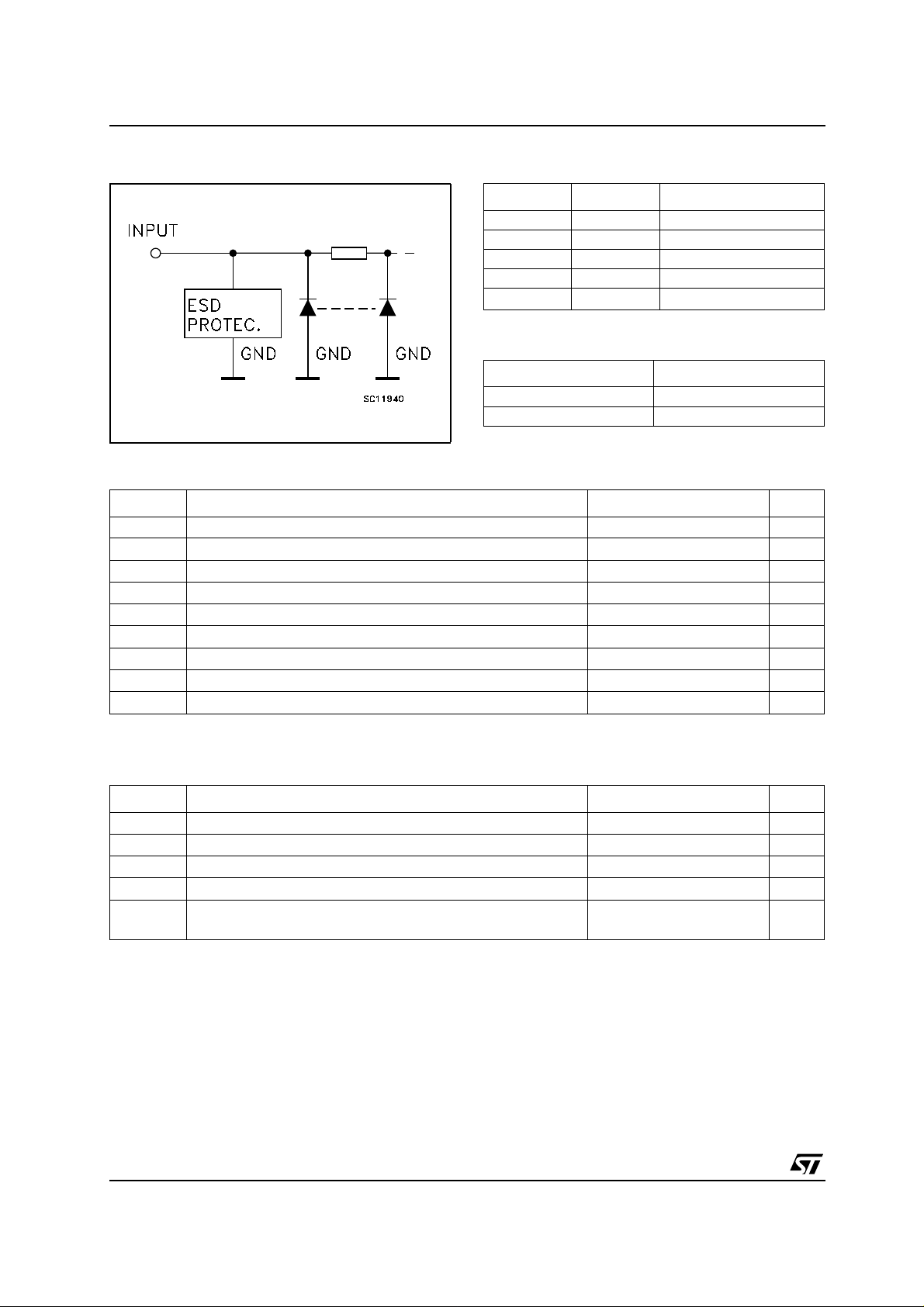
■ POWER DOWN PROTECTION ON INPUT
■ OPERATING VOLTAGE RANGE:
V
(OPR) = 2V to 5.5V
CC
■ IMPROVED LATCH-UP IMMUNITY
= 28% VCC(MIN.)
= 3.7ns (TYP.) at VCC=5V
PD
DESCRIPTION
The 74V1G05 is an advanced high-speed CMOS
SINGLE INVERTER (OPEN DRAIN) fabricated
with sub-micron silicon gate and double-layer
metal wiring C
2
MOS technology.
The internal circuit is composed o f 3 stages
including buffer output, which provide high noise
immunity and stable output.
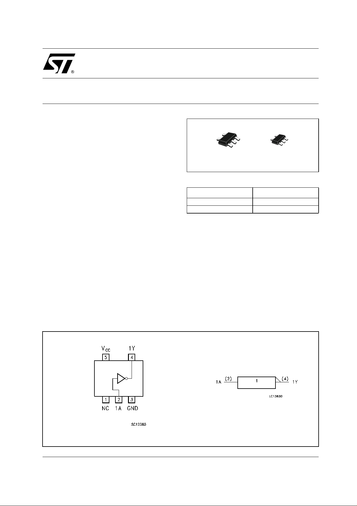
SOT323-5LSOT23-5L
ORDER CODES
PACKAGE T & R
SOT23-5L 74V1G05STR
SOT323-5L 74V1G05CTR
Power down protection is provided on inpu t and 0
to 7V c an be acce pted on input with no regard to
the supply volt age. This device can be used to
interface5Vto3V.
PIN CONNECTION AND IEC LOGIC SYMBOLS
1/9April 2004
Page 2
74V1G05
INPUT EQUIVALENT CIRCUIT PIN DESCRIPTION
PIN N° SYMBOL NAME AND FUNCTION
1 NC Not Connected
2 1A Data Input
4 1Y Data Output
3 GND Ground (0V)
5
TRUTH TABLE
Z: HighImpedance
ABSOLUTE MAXIMUM RATINGS
Symbol Parameter Value Unit
V
V
V
I
I
OK
I
or I
I
CC
T
T
Absolute Maximum Ratings are those values beyond which damage to the device may occur. Functional operation under these conditions is
not implied.
Supply Voltage
CC
DC Input Voltage
I
DC Output Voltage -0.5 to VCC+0.5
O
DC Input Diode Current
IK
DC Output Diode Current
DC Output Current
O
DC VCCor Ground Current
GND
Storage Temperature
stg
Lead Temperature (10 sec)
L
V
CC
Positive Supply Voltage
AY
LZ
HL
-0.5 to +7.0 V
-0.5 to +7.0 V
V
-20 mA
± 20 mA
± 25 mA
± 50 mA
-65 to +150 °C
260 °C
RECOMMENDED OPERATING CONDITIONS
Symbol Parameter Value Unit
V
V
V
T
dt/dv
1) VINfrom30% to 70% ofV
2/9
Supply Voltage
CC
Input Voltage
I
Output Voltage 0 to V
O
Operating Temperature
op
Input Rise and Fall Time (note 1) (V
CC
CC
(V
=5.0± 0.5V)
CC
=3.3± 0.3V)
2to5.5 V
0to5.5 V
CC
-55 to 125 °C
0 to 100
0to20
V
ns/V
ns/V
Page 3
DC SPECIFICATIONS
Symbol Parameter
V
V
High Level Input
IH
Voltage
V
Low Level Input
IL
Voltage
Low Level Output
OL
Voltage
High Impedance
I
OZ
Output Leakage
Current
I
Input Leakage
I
Current
I
Quiescent Supply
CC
Current
Test Condition Value
V
(V)
CC
= 25°C
A
Min. Typ. Max. Min. Max. Min. Max.
-40 to 85°C -55 to 125°C
T
2.0 1.5 1.5 1.5
3.0to
5.5
0.7V
CC
0.7V
CC
0.7V
CC
2.0 0.5 0.5 0.5
3.0to
5.5
2.0
3.0
4.5
3.0
4.5
5.5
0to
5.5
5.5
IO=50 µA
=50 µA
I
O
=50 µA
I
O
=4 mA
I
O
I
=8 mA
O
I=VIH
or V
IL
V
VO=VCCor GND
V
=5.5VorGND
I
V
I=VCC
or GND
0.3V
CC
0.3V
CC
0.0 0.1 0.1 0.1
0.0 0.1 0.1 0.1
0.0 0.1 0.1 0.1
0.36 0.44 0.55
0.36 0.44 0.55
±
0.25
± 2.5 ± 5 µA
± 0.1 ± 1 ± 1 µA
11020µA
74V1G05
Unit
0.3V
CC
V
V
V
AC ELECTRICAL CHARACTERISTICS (Input t
Test Condition Value
Symbol Parameter
t
t
(*) Voltage range is3.3V± 0.3V
(**) Voltage range is 5.0V ± 0.5V
Propagation Delay
PZL
Time
Propagation Delay
PLZ
Time
V
3.3
3.3
5.0
5.0
3.3
5.0
C
CC
(V)
L
(pF)
(*)
15 4.8 7.7 1.0 9.0 1.0 10.0
(*)
50 5.3 8.5 1.0 10.0 1.0 11.0
(**)
15 3.7 5.5 1.0 6.5 1.0 7.5
(**)
50 4.2 7.5 1.0 8.5 1.0 9.5
(*)
50 7.5 10.5 1.0 11.5 1.0 12.5
(**)
50 4.7 7.5 1.0 8.5 1.0 9.5
=3ns)
r=tf
= 25°C
T
A
-40 to 85°C -55 to 125°C
Min. Typ. Max. Min. Max. Min. Max.
Unit
ns
ns
3/9
Page 4

74V1G05
CAPACITIVE CHARACTERISTICS
Test Condition Value
= 25°C
Symbol Parameter
T
A
Min. Typ. Max. Min. Max. Min. Max.
C
C
C
Input Capacitance 4 10 10 10 pF
IN
Output
OUT
Capacitance
Power Dissipation
PD
Capacitance
510 10 10pF
3pF
(note 1)
1) CPDis defined as the value of the IC’s internal equivalent capacitance which is calculated from the operating current consumption without
load. (Refer to Test Circuit). Average operating current can be obtained by the following equation. I
TEST CIRCUIT
-40 to 85°C -55 to 125°C
CC(opr)=CPDxVCCxfIN+ICC
Unit
CL= 15/50pF or equivalent (includes jig and probe capacitance)
R
=1KΩor equivalent
1
R
T=ZOUT
of pulse generator (typically 50Ω)
WAVEFORM: PROPAGATION DELAY (f=1MHz; 50% duty cycle)
4/9
Page 5

74V1G05
SOT23-5L MECHANICAL DATA
mm. mils
DIM.
MIN. TYP MAX. MIN. TYP. MAX.
A 0.90 1.45 35.4 57.1
A1 0.00 0.10 0.0 3.9
A2 0.90 1.30 35.4 51.2
b 0.35 0.50 13.7 19.7
C 0.09 0.20 3.5 7.8
D 2.80 3.00 110.2 118.1
E 1.50 1.75 59.0 68.8
e0.95 37.4
H 2.60 3.00 102.3 118.1
L 0.10 0.60 3.9 23.6
.
7049676C
5/9
Page 6

74V1G05
SOT323-5L MECHANICAL DATA
mm. mils
DIM.
MIN. TYP MAX. MIN. TYP. MAX.
A 0.80 1.10 31.5 43.3
A1 0.00 0.10 0.0 3.9
A2 0.80 1.00 31.5 39.4
b 0.15 0.30 5.9 11.8
C 0.10 0.18 3.9 7.1
D 1.80 2.20 70.9 86.6
E 1.80 2.40 70.9 94.5
E1 1.15 1.35 45.3 53.1
e
e1 1.3 51.2
L 0.10 0.30 3.9 11.8
.65
0
25.6
6/9
Page 7

Tape & Reel SOT23-xL MECHANICAL D ATA
74V1G05
DIM.
MIN. TYP MAX. MIN. TYP. MAX.
A 180 7.086
C 12.8 13.0 13.2 0.504 0.512 0.519
D 20.2 0.795
N 60 2.362
T 14.4 0.567
Ao 3.13 3.23 3.33 0.123 0.127 0.131
Bo 3.07 3.17 3.27 0.120 0.124 0.128
Ko 1.27 1.37 1.47 0.050 0.054 0.0.58
Po 3.9 4.0 4.1 0.153 0.157 0.161
P 3.9 4.0 4.1 0.153 0.157 0.161
mm. inch
7/9
Page 8

74V1G05
Tape & Reel SOT323-xL MECHANICAL DATA
DIM.
MIN. TYP MAX. MIN. TYP. MAX.
A 175 180 185 6.889 7.086 7.283
C 12.8 13 13.2 0.504 0.512 0.519
D 20.2 0.795
N 59.5 60 60.5 2.362
T 14.4 0.567
Ao 2.25 0.088
Bo 2.7 0.106
Ko 1.2 0.047
Po 3.9 4 4.1 0.153 0.157 0.161
P 3.8 4 4.2 0.149 0.157 0.165
mm. inch
8/9
Page 9

74V1G05
Information furnished is believed to be accurate and reliable. However, STMicroelectronics assumes no responsibility for the
consequences of use of such inform ation nor fo r an y infring ement of p atents or o ther rights of third p arties which may r esult f rom
its use. No license is granted by implication or otherwise under any patent or patent rights of STMicroelectronics. Specifications
mentioned in this publication are subject to change without notice. This publication supersedes and replaces all information
previously supplied. STMicroelectronics products ar e not authorized for use as critical components in life support devices or
systems without express written approval of STMicroelectronics.
Australia - Belgium - Brazil - Canada - China - Czech Republic - Finland - France - Germany - Hong Kong - India - Israel - Italy - Japan -
Malaysia - Malta - Morocco - Singapore - Spain - Sweden - Switzerland - United Kingdom - United States.
The ST logo is a registered trademark of STMicroelectronics
All other names are the property of their respective owners
© 2004 STMicroelectronics - All Rights Reserved
STMicroelectronics GROUP OF COMPANIES
http://www.st.com
9/9
 Loading...